

Page 1
SM8230A
NIPPON PRECISION CIRCUITS INC.
OVERVIEW
The SM8230A is a dual-tone signal generator LSI
developed for DTMF (dual tone multi-frequency)
dialing. It features a built-in piezo-electric speaker
driver for direct connection to a piezo-electric
buzzer.
The DTMF frequencies can be set to correspond to
the DTMF standards of any country. The output level
is also adjustable under software control. These
features, combined with its small package and low
power dissipation, make the SM8230A a very use
device to use.
FEATURES
■
3-line serial interface to external CPU
■
2 independent, adjustable frequency outputs
■
Piezo driver for direct connection to a piezoelectric buzzer
■
4 system clock frequencies selectable (480 kHz,
960 kHz, 1.92 MHz, 3.84 MHz)
■
2.6 to 3.3 V supply voltage
■
Low current consumption
• 3.0 mA (max) operating current
• 1 µA (max) standby current
■
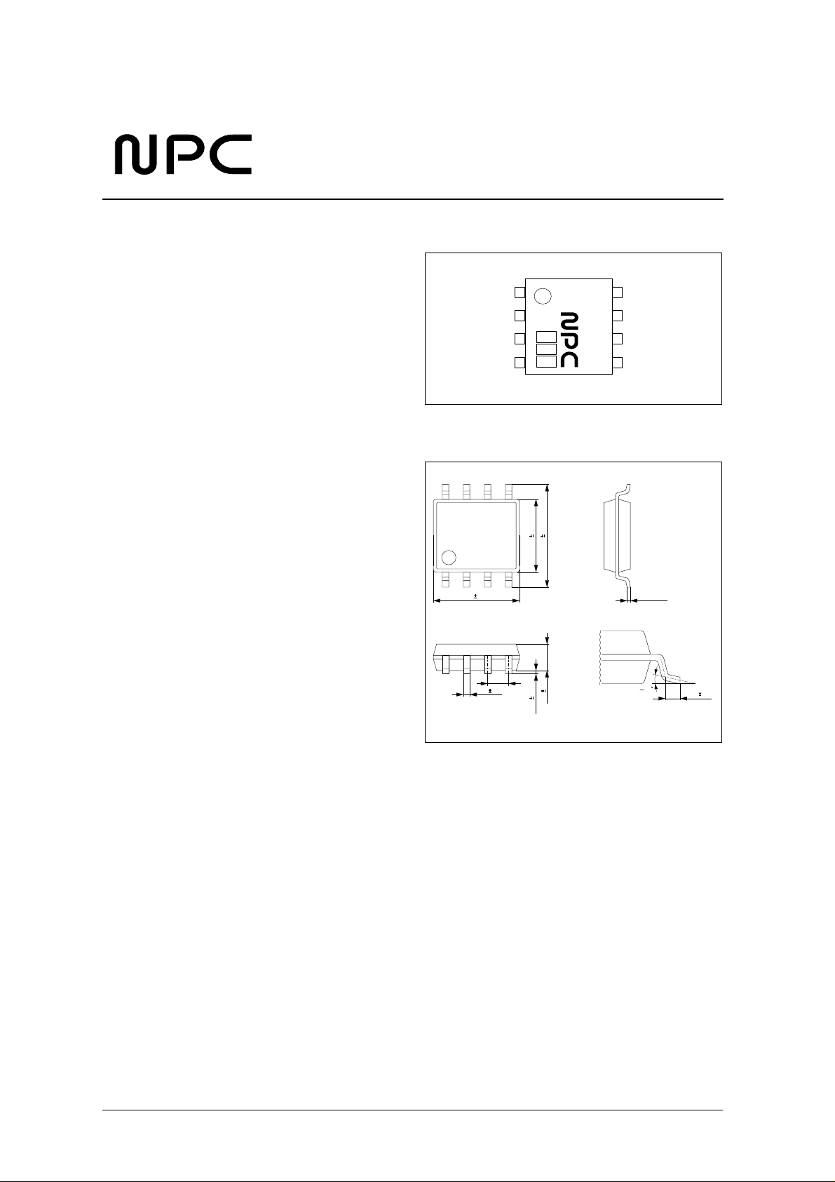
8-pin plastic SOP
Tone Dialer with Built-in Piezo Driver
PINOUT
8230AS
SD
SCL
OE
VSS
PACKAGE DIMENSIONS
4.4 0.2
6.2 0.3
5.2 0.3
1.27
0.4 0.1
1.5 0.1
0.05 0.05
81
VDD
BZH
BZL
CLK
54
+ 0.10
0.15
− 0.05
010
0.4 0.2
NIPPON PRECISION CIRCUITS—1
Page 2
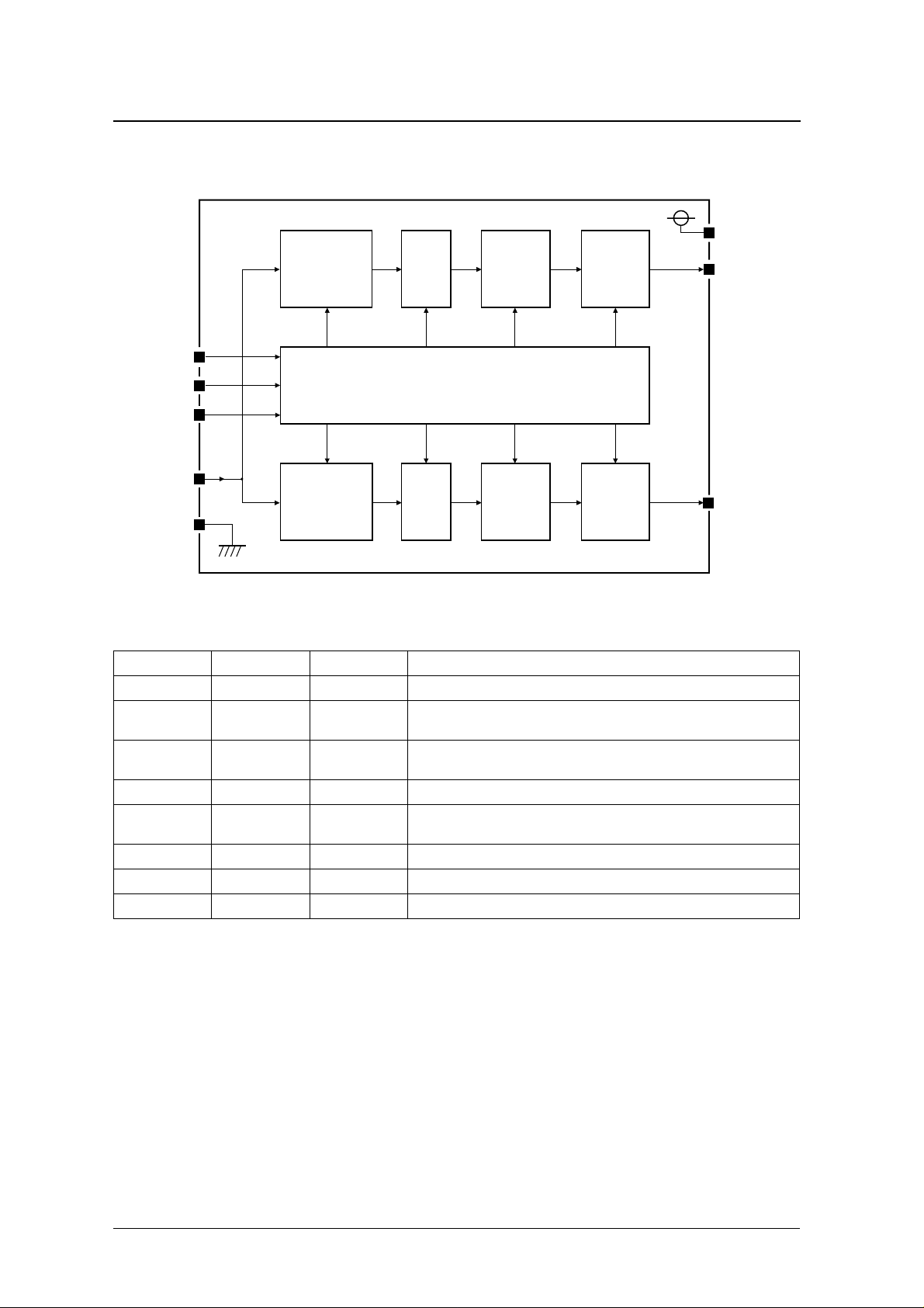
BLOCK DIAGRAM
SD
SCL
OE
Programmable
Counter
High Group
SM8230A
ROM
LATCH
SELECTOR
D/A
Converter
Output
Control
VDD
BZH
CLK
VSS
Programmable
Counter
Low Group
ROM
D/A
Converter
PIN DESCRIPTION
Number Name I/O Description
1 SD I Serial data input
2SCLI
3OEI
4 VSS – Ground
5CLKI
6 BZL O DTMF low-frequency group analog output
7 BZH O DTMF high-frequency group analog output
8 VDD – Supply voltage
Serial data transfer clock input.
(For valid transfer, OE must stay LOW for 16 clock cycles.)
DTMF output enable/serial data transfer select input.
Serial data transfer is selected when LOW.
System clock input. The clock can be set to one of four frequencies (480 kHz, 960
kHz, 1.92 MHz, 3.84 MHz).
Output
Control
BZL
NIPPON PRECISION CIRCUITS—2
Page 3
−
−
−
−
°
°
−
° C
−
−
SM8230A
SPECIFICATIONS
Absolute Maximum Ratings
V
= 0 V
SS
Parameter Symbol Rating Unit
Supply voltage range V
Input voltage range V
Output voltage range V
Storage temperature range T
Power dissipation P
Soldering temperature T
Soldering time t
DD
IN
OUT
stg
D
sld
sld
0.3 to 7.0 V
V
0.3 to V
SS
V
0.3 to V
SS
+ 0.3 V
DD
+ 0.3 V
DD
55 to 125
250 mW
255
10 s
C
C
Recommended Operating Conditions
V
= 0 V
SS
Parameter Symbol Condition
Supply voltage range V
Operating temperature T
DD
opr
DC Characteristics
V
= 2.6 to 3.3V, V
DD
Parameter Symbol Condition
Operating current consumption I
Standby current consumption I
Input voltage (all inputs)
Input leakage current I
BZH/BZL tone output voltage V
BZH/BZL tone output adjustment
step
BZH/BZL tone output absolute error D
BZH/BZL tone output impedance Z
= 0 V, T
SS
= − 20 to 70 ° C
a
DD
ST
V
IH
V
IL
IL
BZO
D
RES
LIN
OUT
V
DD
f
CLK
V
DD
HIGH-level input 1.1 – V
LOW-level input V
HIGH/LOW-level input
0 dB output level 0.86V
V
ZBO
Rating
Unit
min typ max
2.6 3.0 3.3 V
20 25 70
Rating
Unit
min typ max
= 3.0 V , T
= 480 kHz
= 25 ° C,
a
– 1.5 3 mA
= 3.3 V, OE = LOW – – 1 µA
DD
SS
– 0.6
1– 1µA
DD
0.93V
DD
1.0V
DD
Vp-p
– 1.0 – dB
levels
1– 1dB
100 150 200
V
Ω
NIPPON PRECISION CIRCUITS—3
Page 4

AC Characteristics
V
= 2.6 to 3.3V, V
DD
SS
= 0 V, T
= − 20 to 70 ° C
a
SM8230A
∆
Parameter Symbol Condition
Tone output frequency error
Tone distortion
CLK cycle time t
CLK LOW-level pulsewidth t
CLK HIGH-level pulsewidth t
OE setup time t
OE hold time t
SCL cycle time t
SCL LOW-level pulsewidth t
SCL HIGH-level pulsewidth t
Input data setup time t
Input data hold time t
1. T
= -10 to 70 ° C, THD + N (10 Hz to 500 kHz), no load
a
1
System clock input timing
Rating
min typ max
= 3.84 MHz,
f
f
DIS BZH/BZL – 5 10 %
CLK
CLKL
CLKH
SUOE
HDOE
SCL
SCLL
SCLH
SUD
HDD
CLK
no deviation
CLK input waveform
Between OE and SCL
SCL input waveform
Between SD and SCL
– – 0.37 %
250 – – ns
100 – – ns
100 – – ns
100 – – ns
100 – – ns
1––µs
400 – – ns
400 – – ns
100 – – ns
100 – – ns
Unit
CLK
Serial data transfer timing
OE
SCL
SD
tCLKL tCLKH
tCLK
1216
DATA(b15) DATA(b14)
tSCLLtSCLHtSUD
tHDD
tSCLtSUOE
DATA(b0)
tHDOE
NIPPON PRECISION CIRCUITS—4
Page 5

SM8230A
FUNCTIONAL DESCRIPTION
Serial Interface
Data is transferred in 16-bit units by writing commands over a 3-line serial interface comprising OE
Port
Serial Clock
CPU
Command transfer
Data can be transferred when OE goes LOW. Data is
transferred in 16-bit units in sync with the rising
edge of the SCL clock.
Note that when OE is LOW and both SD and SCL
are tied LOW, the current consumption is less than 1
µA (standby mode).
Serial Data
(Clock)
Figure 1. Serial interface connection example
(output enable), SCL (serial clock) and SD (serial
data input). Note that data transfer is unidirectional;
no data is output from the SM8230A. The operating
sequence is described below.
OE
SCL
SD
SM8230
BZH
R
Piezo Buzzer
CLK
BZL
The internal states are undefined when power is first
applied.
DTMF analog signal output
Data transfer stops and DTMF analog signal output
starts when OE goes HIGH, as shown in figure 2.
OE
SCL
SD
BZL
BZH
Serial data transmission
12345678910111213141516
b15 b14 b13 b12 b11 b10 b9 b8 b7 b6 b5 b4 b3 b2 b1 b0
0 0 CK1 CK0 FH1 FH0 GH3 GH2 GH1 GH0 FL1 FL0 GL3 GL2 GL1 GL0
MSB LSB
Figure 2. Serial data transfer timing
Piezo buzzer
output
Low frequency
group output
High frequency
group output
NIPPON PRECISION CIRCUITS—5
Page 6

SM8230A
Transfer Command Specifications
The transfer data code format is shown in figure 3.
Data is transferred with the MSB as the leading bit.
The data sets the input clock, high-frequency group
and low-frequency group frequencies, and the output
levels. The commands are shown in tables 1 to 4.
b15(MSB) b0(LSB)
0 0 CK1 CK0 FH1 FH0 GH3 GH2 GH1 GH0 FL1 FL0 GL3 GL2 GL1 GL0
Low group output level set.
Low group frequency set.
High group output level set.
High group frequency set.
CLK pin input frequency set.
−
−
−
−
−
Set (b14, b15) = (0, 0)
for normal operation.
Figure 3. Transfer command format
CK command (CK1, CK0)
These bits set the frequency of the input clock on
CLK. The frequency can be set to 1 × , 2 × , 4 × , and 8 ×
multiples of 480 kHz. The input code and the corresponding clock frequency are shown in table 1.
Table 1. CK command
CK 1 CK 0 CLK input clock frequency
0 0 480 kHz
0 1 960 kHz
1 0 1.92 MHz
1 1 3.84 MHz
FH/FL command (HF1, FH0 / FL1, FL0)
These bits set the DTMF signal high-frequency and
low-frequency group frequencies, respectively.
The input code, the corresponding group frequency
specification, the design value and frequency deviation are shown in tables 2 and 3.
Note that the design value and frequency deviation
are calculated values assuming a deviation-free system clock input on CLK.
Table 2. FH command
FH1 FH0
0 0 1209 1212.1 +0.26
0 1 1336 1333.3
1 0 1477 1481.5 +0.30
DTMF
frequency
(Hz)
Design
value (Hz)
De viation
(%)
0.20
1 1 1633 1632.7
Table 3. FL command
FH1 FH0
0 0 697 697.7 +0.10
0 1 770 769.2
1 0 852 851.1
1 1 941 937.5
DTMF
frequency
(Hz)
NIPPON PRECISION CIRCUITS—6
Design
value (Hz)
0.02
De viation
(%)
0.10
0.11
0.37
Page 7

SM8230A
GH/GL command (GH3 to GH0, GL3 to GL0)
These bits set the output levels of the high-frequency
group and low-frequency group outputs, respectively. The input code and the corresponding output
level are shown in table 4. Note that the 0 dB point is
typically 93% of the supply voltage. Any value
above 0 dB results in amplitude clipping of the output waveform.
Table 4. GH/GL command
GH3/GL3GH2/GL2GH1/GL1GH0/GL0Output
0000 − 9 dB
0001 − 8 dB
0010 − 7 dB
0011 − 6 dB
0100 − 5 dB
0101 − 4 dB
0110 − 3 dB
0111 − 2 dB
1000 − 1 dB
10010 dB
10101 dB
10112 dB
11003 dB
11014 dB
11105 dB
level
11116 dB
NIPPON PRECISION CIRCUITS INC. reserves the right to make changes to the products described in this data sheet in order to
improve the design or performance and to supply the best possible products. Nippon Precision Circuits Inc. assumes no responsibility for
the use of any circuits shown in this data sheet, conveys no license under any patent or other rights, and makes no claim that the circuits
are free from patent infringement. Applications for any devices shown in this data sheet are for illustration only and Nippon Precision
Circuits Inc. makes no claim or warr anty that such applications will be suitab le for the use specified without further testing or modification.
The products described in this data sheet are not intended to use for the apparatus which influence human lives due to the failure or
malfunction of the products. Customers are requested to comply with applicable laws and regulations in effect now and hereinafter,
including compliance with export controls on the distribution or dissemination of the products. Customers shall not expor t, directly or
indirectly, any products without first obtaining required licenses and approvals from appropriate government agencies.
NIPPON PRECISION CIRCUITS INC.
4-3, 2-chome Fukuzumi
Koutou-ku, Tokyo 135-8430, Japan
NIPPON PRECISION CIRCUITS INC.
Telephone: 03-3642-6661
Facsimile: 03-3642-6698
NC9614BE 1997.01
NIPPON PRECISION CIRCUITS—7
 Loading...