

Page 1
SM8224B
NIPPON PRECISION CIRCUITS INC.
Dual-Tone Receiver IC
OVERVIEW
The SM8224B is a receiver and decoder that supports the Bellcore TR-NWT-000030 and SR-TSV-002476
standards calling number identification (caller ID) and call waiting dual-tone signals. It has separate caller ID
signal and call waiting signal inputs, which allows the gain for each input to be adjusted independently. It is
fabricated in CMOS and features a power-down function, realizing low power dissipation operation.
FEATURES
■
TR-NWT-000030 and SR-TSV-002476 standards
(Bellcore)
■
Call waiting
■
FSK decoder
■
High input sensitivity
■
Independent input gain adjustment for caller ID
signal and call waiting signal inputs
■
Power-down mode
■
Crystal oscillator circuit built-in
■
Single supply operation:4.5 to 5.5V
■
Molybdenum-gate CMOS process
APPLICATIONS
■
Telephones, fax machines and modems that support pre- and mid-conversation information services
■
Adapters for pre- and mid-conversation information service functions
■
Telephone answering machines
■
Facsimile machines
■
Computer peripheral equipment
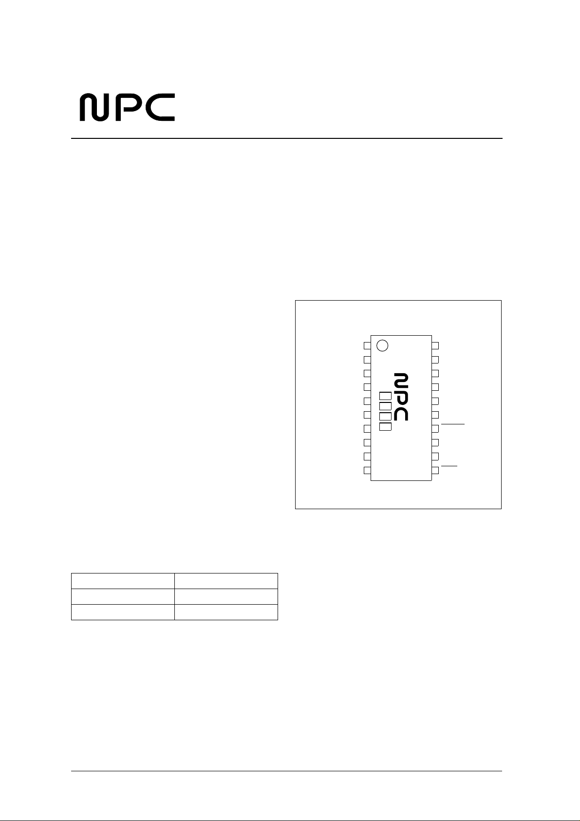
PINOUT
(Top view)
OSCOUT
AGND
TIP
RING
TRQ
GND
OSCIN
MODE
TEST
DOUT
1
20
DT1
DT2
SM8224B
DTQ
S0
S1
VDD
CDET
CR
DTDET
10
11
STR
ORDERING INFORMATION
De vice Pack ag e
SM8224BM 20-pin SSOP
SM8224BS 20-pin SOP
NIPPON PRECISION CIRCUITS—1
Page 2
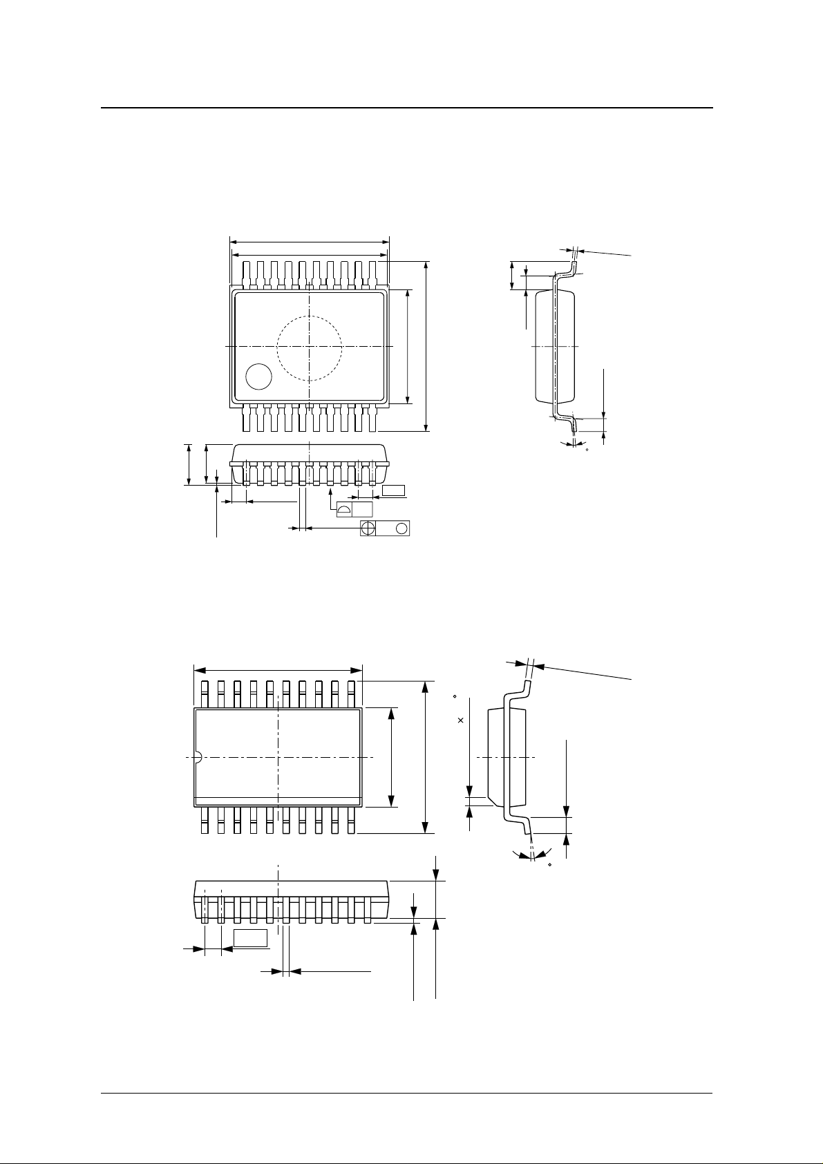
PACKAGE DIMENSIONS
(Unit: mm)
20-pin SSOP
SM8224B
20-pin SOP
2.10 max
1.80 ± 0.10
0.10 ± 0.10
0.68 ± 0.12
7.40 max
7.20 ± 0.05
0.30 ± 0.10
0.10
0.13
0.65
M
5.30 ± 0.05
7.90 ± 0.20
1.30 ± 0.10
0.62 typ
0 to 8
0.20
±
0.6 ± 0.15
0.05
12.75 ± 0.10
1.27
0.41 ± 0.05
7.50 ± 0.10
10.31 ± 0.20
2.34 ± 0.10
0.20 ± 0.10
0.275 ± 0.045
0.51 ± 0.2 45
0.76 ± 0.25
0 to 8
NIPPON PRECISION CIRCUITS—2
Page 3
BLOCK DIAGRAM
SM8224B
TIP
RING
TRQ
DT1
DT2
DTQ
AGND
Bias
Circuit
Crystal
Oscillator
Circuit
Filter
Filter
Filter
(2130Hz)
Filter
(2750Hz)
Power-down
Circuit
FSK
Demodulator
Carrier
Detector
Detector
Circuit
(2130Hz)
Level
Detector
Detector
Circuit
(2750Hz)
Level
Detector
Output
Circuit
Time-constant
Circuit
DOUT
CDET
STR
CR
DTDET
OSCIN OSCOUT MODE GNDVDD
S0
S1
NIPPON PRECISION CIRCUITS—3
Page 4
SM8224B
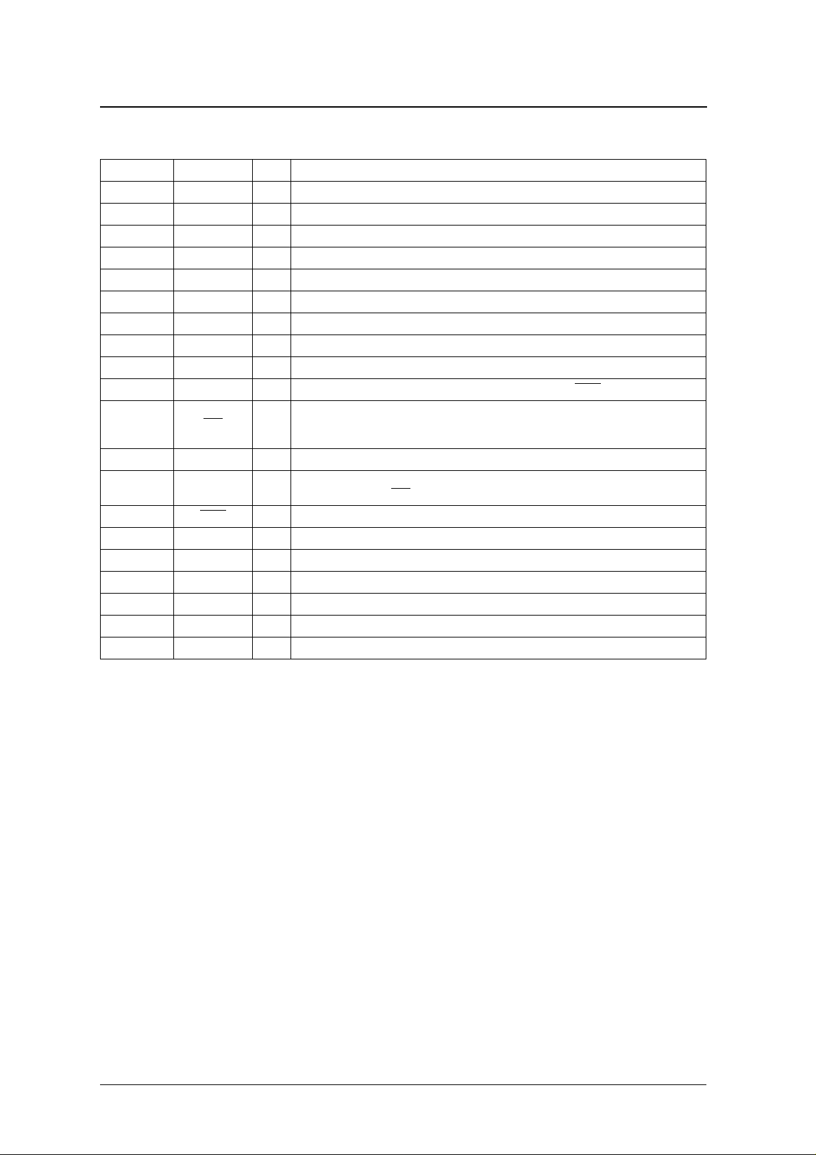
PIN DESCRIPTION
Number Name I/O Function
1 AG N D O Analog ground output. Internal reference voltage (V
2 TIP I Tip input. Connected to the telephone line through a protection circuit
3 RING I Ring input. Connected to the telephone line through a protection circuit
4 T R Q O Input-stage amplifier gain-select output. Used to adjust the gain of the input-stage amplifier.
5 G ND – Ground. Connected to the system ground potential.
6 OSCIN I Crystal oscillator input. The cr ystal oscillator element is connected between this pin and OSCOUT.
7 OSCOUT O Crystal oscillator output. The crystal oscillator element is connected between this pin and OSCIN.
8 MODE I When MODE is HIGH, and S1 and S0 are both LOW, the device is in power-down state. See table 2.
9 TEST – TEST pin. Set OPEN when normal using.
10 DOUT O Data output. Demodulated FSK signal output. HIGH level output when CDET goes HIGH.
11 STR O
12 DTDET O Dual-tone detector output. HIGH-level output when dual tone is detected.
13 C R I/O
14 CDET O FSK signal carrier detector output. L OW -level when active carrier is detected.
15 VD D – Supply
16 S1 I Function select bit 1. Selects the device mode in combination with S0 and MODE. See table 2.
17 S0 I Function select bit 1. Selects the device mode in combination with S1 and MODE. See table 2.
18 D TQ O Dual-tone signal input-stage amplifier output. Used to adjust the gain of the input-stage amplifier.
19 DT 2 I Dual-tone signal input-stage operational amplifier inverting input
20 DT 1 I Dual-tone signal input-stage operational amplifier non-inverting input
Dual-tone confirmation output. Function is selected by S0 and S1. See table 2.
Dual-tone confirmation: Active-LOW output when dual tone detection signal passes through RC time
constant delay circuit.
Dual tone RC time constant circuit connection. The dual tone detection signal passes through the RC
network to generate the ST R signal.
/2) output level
DD
NIPPON PRECISION CIRCUITS—4
Page 5

−
−
−
° C
∆
−
−
° C
SPECIFICATIONS
Absolute Maximum Ratings
GND = 0V
Parameter Symbol Condition Rating Unit
Supply voltage range V
Input voltage range V
Po w er dissipation P
Storage temperature range T
Recommended Operating Conditions
GND = 0V
DD
IN
D
stg
SM8224B
−
−
0.5 to 7.0 V
0.3 to V
+ 0.3 V
DD
44 m W
40 to 125
Parameter Symbol Condition
Supply voltage V
Clock frequency f
Clock frequency accuracy
Operating temperature T
Electrical Characteristics
V
= 5.0V ± 0.5V, GND = 0V, f
DD
Parameter Symbol Condition
Supply current consumption I
Pow er-down current I
MODE, S0, S1 LOW -level input
voltage
MODE, S0, S1 HIGH-level input
voltage
OSCIN LOW-level input voltage V
OSCIN HIGH-level input voltage V
DOUT, STR, DTDET, CR, CDET
L O W-level output current
DOUT, STR
HIGH-level output current
TIP, RING, DT1, DT2, MODE, S1,
S0 input leakage current
, DTDET, CR, CDET
DD
CLK
f
C
opr
= 3.579545MHz, T
CLK
No analog signal input, no output load,
DD
S1 = 0V, S0 = V
No analog signal input, other inputs =
V
DPD
V
V
I
OL
I
OH
I
IL1
IH1
IL2
IH2
IN
or 0V, no output load, S1 = 0V,
DD
S0 = 0V, MODE = V
min typ ma x
4.5 – 5.5 V
– 3.579545 – MH z
0.1 – +0.1 %
20 – 85
= − 20 to 85 ° C unless otherwise noted.
a
min typ ma x
, MODE = 0V
DD
– – 8.0 m A
––15µA
DD
– – 0.3V
0.7V
DD
– – 0.3V
0.7V
DD
2––mA
––
1– 1µA
Rating
Unit
Rating
Unit
DD
V
––V
DD
V
––V
0.8 mA
NIPPON PRECISION CIRCUITS—5
Page 6

– − 43 −
SM8224B
AC Electrical Characteristics
Measurement conditions: R1 = 430k Ω , R2 = 34k Ω , R3 = 390k Ω , C1= 0.22 µ F
FSK decoder
V
= 5.0V ± 0.5V, GND = 0V, f
DD
= 3.579545MHz, T
CLK
= − 20 to 85 ° C unless otherwise noted.
a
−
− 50 −
−
−
−
Parameter Symbol Condition
Input sensitivity –
1
S/N ratio
Carrier detection sensitivity C D
Carrier non-detection sensitivity C D
Oscillator frequency f
1. Ma rk signal and SPACE signal are same level.
Noise: Random noise from 200Hz to 3400Hz.
FSKSNR 20 – – dB
ON
OFF
CLK
typ
min typ m ax
0.1% 3.579545 typ + 0.1% M Hz
Rating
43 CD
46 – dBm
ON
37.78 dB m
Unit
dBm
Dual tone detector
V
= 5.0V ± 0.5V, GND = 0V, f
DD
Parameter Symbol Condition
Frequency (low frequency) f
Frequency (high frequency) f
Detection frequency deviation 1.1 – – %
Non-detection frequency deviation 3.5 – – %
Detection sensitivity
Non-detection sensitivity ––
Signal level deviation ––6dB
= 3.579545MHz, T
CLK
L
H
= − 20 to 85 ° C unless otherwise noted.
a
Rating
min typ m ax
– 2130 – Hz
– 2750 – Hz
37.78 – – dB m
43.78 dB m
Unit
Note: (S0, S1, MODE) = (V
, 0V, 0V)
DD
Input-stage amplifier Characteristics
V
= 5.0V ± 0.5V, GND = 0V, f
DD
Parameter Symbol Condition
Input leakage current I
DC open-loop voltage gain G
Unity gain frequency f
Load capacitance C
Load resistance R
= 3.579545MHz, T
CLK
IN
OL
C
L
L
= − 20 to 85 ° C unless otherwise noted.
a
Rating
min typ m ax
––1µA
30 – – dB
80 – – kHz
– – 100 pF
50 – – k Ω
NIPPON PRECISION CIRCUITS—6
Unit
Page 7

Timing Characteristics
FSK decoder
V
= 5.0V ± 0.5V, GND = 0V, f
DD
= 3.579545MHz, T
CLK
SM8224B
= − 20 to 85 ° C unless otherwise noted.
a
Parameter Symbol Condition
Pow er-down release to start-up time t
Carrier detection ON time t
Final data to carrier detection OFF time t
DOSC
DAQ
DCH
min typ m ax
–5–ms
2.5 – 10 m s
3–15ms
Rating
Unit
Output timing)
V
= 5.0V ± 0.5V, GND = 0V, f
DD
= 3.579545MHz, T
CLK
= − 20 to 85 ° C, FSK input data = 1200 ± 12 baud
a
unless otherwise noted.
Parameter Symbol Condition
STR, DOUT rise time t
STR, DOUT fall time t
Input/output delay t
DOUT data rate 1188 1200 1212 baud
r0
f0
IDD
Input to DOUT – – 5 m s
min typ m ax
– – 200 ns
– – 200 ns
Rating
Unit
NIPPON PRECISION CIRCUITS—7
Page 8

TIMING DIAGRAMS
FSK demodulator timing
SM8224B
1st Ring
L1/L2
PDWN
CDET
DOUT
OSCOUT
P DWN is an inter nal signal (set by S0, S1, MODE)
Output timing
DOUT
tDOSC
101010... 1 Data
tDAQ
101010...1
Data
2nd Ring
tDCH
DOUT
STR
Data timing
TIP/RING
STR
DOUT
90%
10%
tr0 tf0
90%
10%
tf0 tr0
START
STOP
0 b0 b1 b2 b3 b4 b5 b6 b7 1 0 b0 b1 b2 b3 b4b6 b7 1 b5 b6
STOP
START
tIDD
START
b4 b5 b6 b7 b0 b1 b2 b3 b4 b5 b6 b7 b0 b1 b2 b3 b4
STOP
NIPPON PRECISION CIRCUITS—8
Page 9

FUNCTIONAL DESCRIPTION
SM8224B
The SM8224B receiver with caller ID service conforms to the Bellcore standards. It incorporates FSK
demodulator and dual-tone detection functions in a
single chip. It has a dedicated dual-tone signal input
tone signal input amplification can be set independently. This allows systems can be easily constructed
that provide pre- and mid-conversation information
services.
so that the FSK signal input amplification and dual-
FSK Demodulator
Calling number identification service is sent as an
FSK signal, and the SM8224B FSK demodulator
processes this signal.
The FSK signal conforms to the following Bellcore
standard.
Table 2. Function select
S1 S0 MODE Function ST R
LOW LOW HIGH Power-down HIGH
HIGH LOW LOW Dual-tone detection from DT1/DT2
LOW HIGH LOW FSK and dual-tone detection from TIP/RING L OW (dual tone confirmation)
HIGH HIGH LOW FSK detection from TIP/RING HIGH
LO W LO W L OW Test mode
1. DT1, DT2, DTQ are active in this mode only.
2. Test mode should not be used.
Note: S1, S0, MODE setting should be used from above combination except Test mode.
2
Table 1. FSK signal
Parameter Description
Modulation type
Logic “1” data (mar k) 1200 ± 12 Hz
Logic “0” data (space) 2200 ± 22 Hz
Signal level (mark)
Signal level (space)−36 to −12 dBm
Data transfer rate 1200 ± 12 baud
1
Continuous-phase binary frequency-shiftkeying
−
32 to −12 dBm
LO W (dual tone confirmation)
Dual T one Detector
When using mid-conversation information services,
2 mixed signals of 2130Hz and 2750Hz are sent on
lines L1 and L2. The SM8224B detects the 2 signals
from the background noise. It uses 2 separate highorder filters with center frequencies of 2130Hz and
2750Hz to detect the presence of the signal frequencies.
In series with the filters are level detectors. When the
input level exceeds the preset rating, the signal is
detected. When the input level is below the rating,
the signal is not detected.
If both the 2130Hz and 2750Hz signals are simultaneously detected, DTDET goes HIGH and starts
charging the time constant circuit comprised by an
external capacitor and external resistor. When the
time constant circuit voltage rises above a fixed voltage level, STR signal goes LOW to indicate dual
tone detection.
NIPPON PRECISION CIRCUITS—9
Page 10

TYPICAL APPLICATION CIRCUIT
Speech
Network
Circuit
Protection
Circuit
L1
L2
R1
1%
C1
5%
R1
C1
1%
5%
VDD
R6
1%
C2
5%
C2
R6
5%
VDD
1%
R2
1%
R9
1%
R5
1%
R2
1%
0.1µF
20%
SM8224B
R8
1%
R4
1%
R3
1%
AGND
TIP
RING
TRQ
GND
OSCIN
OSCOUT
MODE
TEST
DOUT
DT1
DT2
DTQ
VDD
CDET
CR
DTDET
STR
R7
1%
S0
S1
VDD
0.1µF
20%
Note : Please set this capacitor
nearby IC pin.
Symbol Rating
R
1
R
2
R
3
C
1
R
4
R
5
R
6
R
7
C
2
R
8
R
9
1. Circuit values are preliminary.
1
330 k
27 k
220 k
0.001
47.5 k
60.4 k
430 + 34 k
390 k
0.22
52.3 k
60.4 k
Unit
Ω
Ω
Ω
µ
F
Ω
Ω
Ω
Ω
µ
F
Ω
Ω
NIPPON PRECISION CIRCUITS—10
Page 11

SM8224B
NIPPON PRECISION CIRCUITS INC. reserves the right to make changes to the products described in this data sheet in order to
improve the design or performance and to supply the best possible products. Nippon Precision Circuits Inc. assumes no responsibility for
the use of any circuits shown in this data sheet, conveys no license under any patent or other rights, and makes no claim that the circuits
are free from patent infringement. Applications for any devices shown in this data sheet are for illustration only and Nippon Precision
Circuits Inc. makes no claim or warranty that such applications will be suitable for the use specified without further testing or modification.
The products described in this data sheet are not intended to use for the apparatus which influence human lives due to the failure or
malfunction of the products. Customers are requested to comply with applicable laws and regulations in effect now and hereinafter,
including compliance with export controls on the distribution or dissemination of the products. Customers shall not export, directly or
indirectly, any products without first obtaining required licenses and approvals from appropriate government agencies.
NIPPON PRECISION CIRCUITS INC.
4-3, Fukuzumi 2-chome
Koto-ku, Tokyo 135-8430, Japan
NIPPON PRECISION CIRCUITS INC.
Telephone: 03-3642-6661
Facsimile: 03-3642-6698
NC9910AE 2000.02
NIPPON PRECISION CIRCUITS—11
 Loading...