

Page 1
SM8222A/B
NIPPON PRECISION CIRCUITS INC.
OVERVIEW
The SM8222A/B is a calling number identification
(caller ID) and call waiting signal (dual tone signal)
receiver decoder IC that conforms with the TRNWT-000030 and SR-TSV-002476 (Bellcore) dialer
FEATURES
■
Conforms to TR-NWT-000030 and SR-TSV002476 (Bellcore) standards
■
Call waiting
■
FSK demodulator
■
Ring signal detect circuit built-in
■
High input sensitivity
■
Input gain adjust circuit built-in
■
Power-down mode
APPLICATIONS
Caller ID Service IC with Call Waiting
telephone number display standards. It is implemented in CMOS and incorporates a power-down
function for low power operation.
■
Crystal oscillator circuit built-in
■
Single supply operation
■
Microcontroller I/O interface
■
Molybdenum-gate CMOS process
■
24-pin SOP and 24-pin DIP packages
■
SM8222A : 2.7 to 3.3V operation
■
SM8222B : 4.5 to 5.5V operation
■
Telephones that display dialer number before and
during conversation
■
Adapters to display dialer number before and dur-
■
Answering machines
■
Facsimile machines
■
Computer peripheral devices
ing conversation
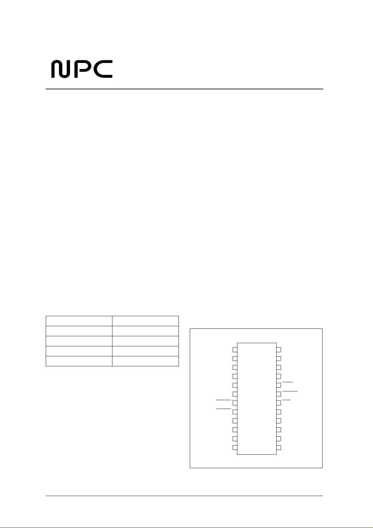
ORDERING INFORMATION PINOUT
De vice Pack age
SM8222AS 24-pin SOP
SM8222AP 24-pin DIP
SM8222BS 24-pin SOP
SM8222BP 24-pin DIP
preliminary
(T op V iew)
OSCOUT
TIP
RING
GS
AGND
CAP
RDIN
RDRC
RDET
MODE
OSCIN
GND
1
12
24
13
VDD
STGT
EST
STD
INT
CDET
DR
DOUT
DCLK
FSKEN
PDWN
IC
NIPPON PRECISION CIRCUITS—1
Page 2
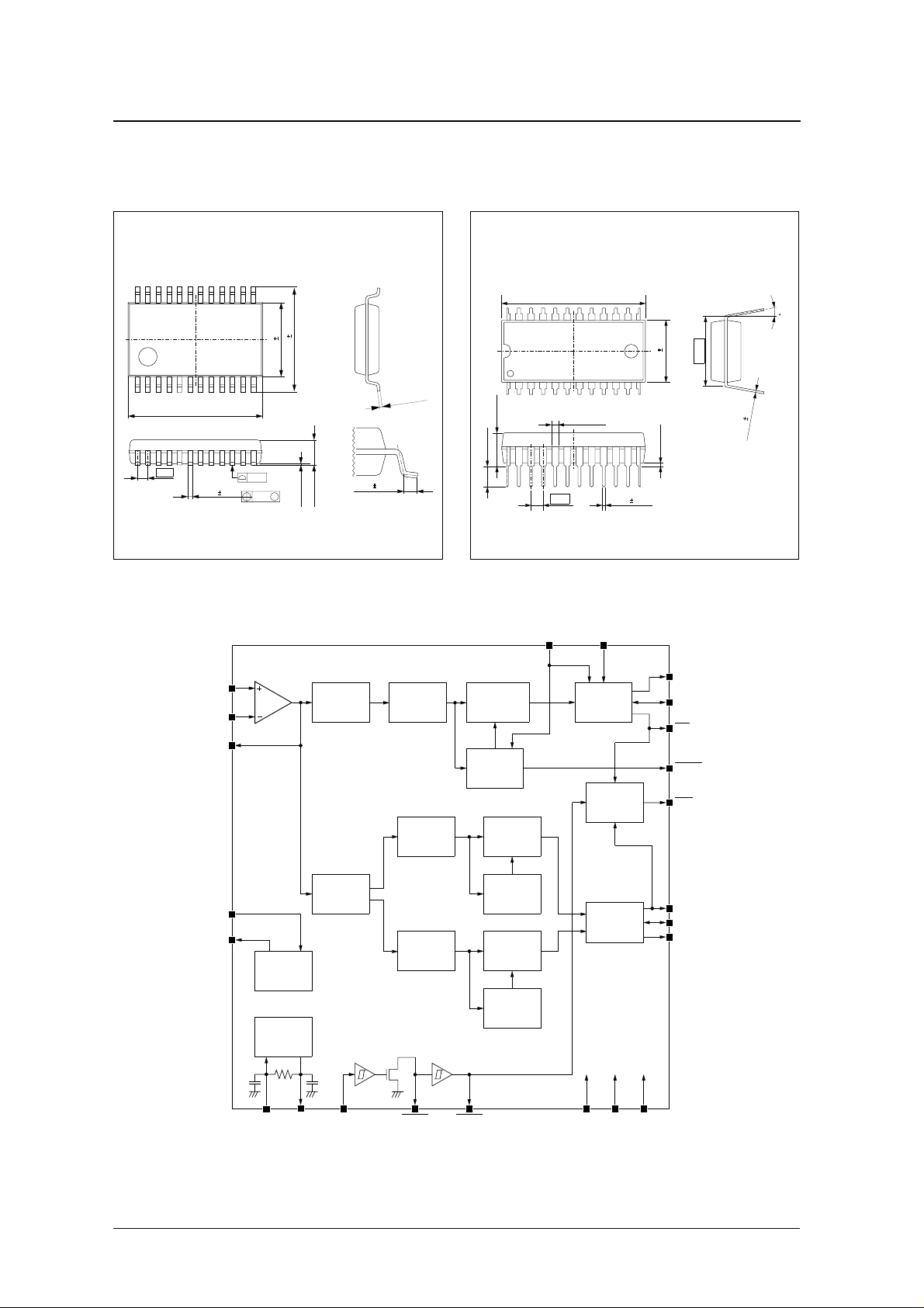
PACKAGE DIMENSIONS
(Unit: mm)
SM8222A/B
24-pin SOP
+ 0.25
15.24
− 0.20
1.27
0.45 0.10
0.10
0.13
BLOCK DIAGRAM
TIP
RING
GS
7.60 0.30
M
10.20 0.40
0.05min
2.80max
Amplifier
0.50 0.20
0.15
0.05
+
0.02
−
Filter
Filter
(2130Hz)
24-pin DIP
4.96max
3.00min
FSK
Demodulator
Carrier
Detector
Data
Detector
(2130Hz)
30.20
2.54
+ 0.20
− 0.30
+ 0.50
1.50
− 0
Data Timing
MODEFSKEN
Control
Interrupt
Generator
0.45 0.08
13.55 0.25
0.51min
DOUT
DCLK
DR
CDET
INT
15 max
15.24
0.25 0.05
CAP
AGND
Level
Detector
Data
Detector
(2750Hz)
Level
Detector
Guard Time
Control
STD
STGT
EST
Bias
Generator
Oscillator
Filter
Filter
(2750Hz)
preliminary
OSCIN OSCOUT RDIN
RDRC RDET
GNDVDDPDWN
NIPPON PRECISION CIRCUITS—2
Page 3
SM8222A/B
PIN DESCRIPTION
Number Name I/O Description
1 TIP I Tip input: Connected to the telephone through a protection circuit.
2 RING I Ring input: Connected to the telephone through a protection circuit.
3 GS O Input stage amplifier output: Used to select the input amplifier gain
4 AGND O Analog ground: Internal reference voltage (V
5 CAP I Reference voltage capacitor connection. C = 0.1 µF
6 RDIN I
7 RDRC
8 RDET
9 MODE I
10 OSCIN I Crystal oscillator element input: Oscillator element connection between OSCIN and OSCOUT.
11 OSCOUT O Crystal oscillator element output: Oscillator element connection between OSCIN and OSCOUT.
12 GND – Ground: Connect to system ground.
13 IC I Test input: Tie LOW for normal operation.
14 PDWN I
15 FSKEN I
16 DCLK I/O
17 DOUT O
18 DR
19 CDET
20 INT O Interrupt signal output: Goes LOW when either RDET is LOW, DR is LOW or STD is HIGH.
21 STD O
22 EST O Dual tone detect output: Goes HIGH when the dual tone is detected.
23 STGT I/O
24 VDD – Supply voltage
Ring detect input: Line reversal and ring signal detect input. Connect to detect attenuated ring
signals. Schmitt-trigger input.
Ring detect RC connection: RC network connection to set the ring detect delay time. Open-drain
I/O
output and schmitt-trigger input.
O Ring detect output: RDRC schmitt-trigger buffer output. LOW when a ring signal is detected.
FSK interface mode select: Demodulated FSK signal output method select.
LOW [Mode = 0]: Demodulated data output and data sync clock output.
HIGH [Mode = 1]: Data output in sync with an external clock.
Power-down control: LOW for normal operation. HIGH for device power-down state. When device is
powered-down, AGND, OSCOUT, DCLK, DOUT, INT, CDET are all HIGH. DR also goes HIGH in
mode 0 output. Schmitt-trigger input.
FSK signal output control: Demodulated FSK signal output and carrier detect output control.
Mode 0: DCLK, DOUT, DR, CDET control
Mode 1: DCLK, DOUT, CDET control
FSK signal reception enabled when HIGH.
Signal pins (above) go HIGH when FSKEN is LOW.
FSK interface clock: Demodulated FSK signal output clock.
Mode 0: Clock output in sync with data
Mode 1: Data read clock input
Data output: Demodulated FSK signal output. HIGH-le v el output when PD WN is HIGH or FSKEN is
LOW, or when CDET
Data output trigger: Demodulated FSK data timing output. Active-LOW. Becomes active when 8 bits
O
of data are completed.
O Carrier (FSK signal) detect output: Goes LOW when a valid carrier signal is detected.
Dual tone indicator output: Goes HIGH if the dual tone detect signal is recognized after the external
RC circuit time delay has elapsed.
Dual tone RC time constant circuit connection: External RC network connection for dual tone signal
detection processing. Sets STD output.
is HIGH in receive state.
/2) output.
DD
preliminary
NIPPON PRECISION CIRCUITS—3
Page 4
−
−
−
+
−
° C
∆
−
−
°
SPECIFICATIONS
Absolute Maximum Ratings
GND = 0 V
Parameter Symbol Condition Rating Unit
Supply voltage range V
Input voltage range V
Input current I
Power dissipation P
Storage temperature range T
DD
IN
IN
D
stg
Recommended Operating Conditions
SM8222A
SM8222B
SM8222A/B
0.5 to 5.0
0.5 to 7.0
0.3 to V
0.3 V
DD
10 mA
44 mW
40 to 125
V
GND = 0 V
Parameter Symbol Condition
Supply voltage range V
Clock frequency f
Clock frequency accuracy
Operating temperature T
DD
CLK
opr
Rating
min typ ma x
SM8222A 2.7 – 3.3
SM8222B 4.5 – 5.5
– 3.579545 – MHz
f
C
0.1 – +0.1 %
20 – 85
Unit
V
C
preliminary
NIPPON PRECISION CIRCUITS—4
Page 5
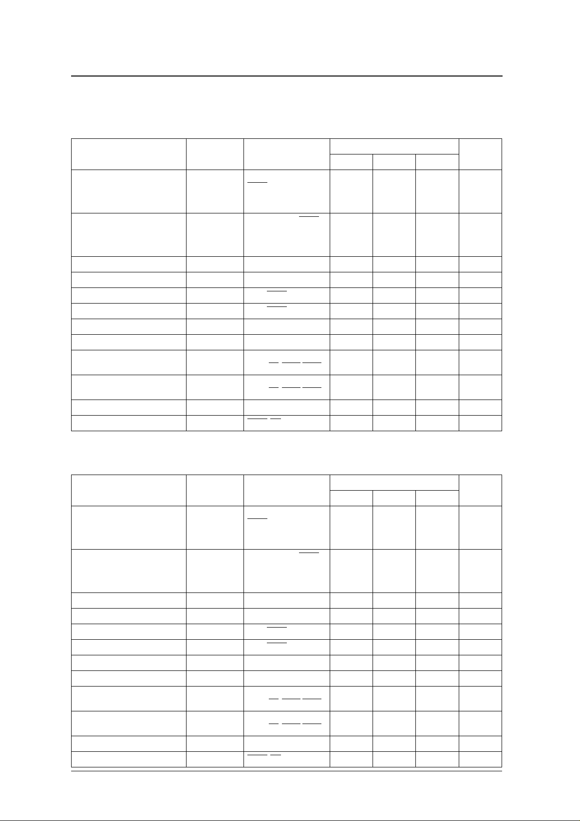
DC Electrical Characteristics
SM8222A
■
V
= 3.0 ± 0.3 V, GND = 0 V, f
DD
Parameter Symbol Condition
Current consumption I
Power-down current consumption I
LOW-level input v oltage 1 V
HIGH-level input voltage 1 V
LOW-level input v oltage 2 V
HIGH-level input voltage 2 V
LOW-level input v oltage 3 V
HIGH-level input voltage 3 V
LOW-level output current I
HIGH-level output current I
Input leakage current I
Output leakage current I
CLK
DPD
SM8222A/B
= 3.579545 MHz, T
OSCIN = PWDN = RDIN =
RDRC
DD
IL1
IH1
IL2
IH2
IL3
IH3
OL
OH
IN
OFF
= MODE = 0 V,
FSKEN = V
inputs open
OSCIN = RDIN = RDRC
MODE = 0 V, PWDN =
FSKEN = V
inputs open
PWDN, MODE, FSKEN – – 0.3V
PWDN, MODE, FSKEN 0.7V
RDIN, RDRC
RDIN, RDRC
OSCIN – – TBD V
OSCIN T BD – – V
DOUT, EST, STD, STGT,
DCLK, DR
DOUT, EST, STD, STGT,
DCLK, DR
OSCIN, PWDN, RDIN
RDRC
, INT ––1µA
= − 20 to 85 ° C
a
, all other
DD
, all other
DD
, RDET, CDET
, RDET, CDET
−
−
min typ max
– 2.5 4.5 mA
=
––15µA
DD
– – 0.3V
0.7V
DD
2––mA
––−0.8 mA
1– 1µA
Rating
DD
––V
DD
––V
Unit
V
V
■
SM8222B
V
= 5.0 ± 0.5 V, GND = 0 V, f
DD
Parameter Symbol Condition
Current consumption I
Power-down current consumption I
LOW-level input v oltage 1 V
HIGH-level input voltage 1 V
LOW-level input v oltage 2 V
HIGH-level input voltage 2 V
LOW-level input v oltage 3 V
HIGH-level input voltage 3 V
preliminary
LOW-level output current I
HIGH-level output current I
Input leakage current I
Output leakage current I
= 3.579545 MHz, T
CLK
OSCIN = PWDN = RDIN =
DD
DPD
IL1
IH1
IL2
IH2
IL3
IH3
OL
OH
IN
OFF
RDRC = MODE = 0 V,
FSKEN = V
inputs open
OSCIN = RDIN = RDRC =
MODE = 0 V, PWDN =
FSKEN = V
inputs open
PWDN, MODE, FSKEN – – 0.3V
PWDN, MODE, FSKEN 0.7V
RDIN, RDRC – – 0.3V
RDIN, RDRC 0.7V
OSCIN – – TBD V
OSCIN T BD – – V
DOUT, EST, STD, STGT,
DCLK, DR, RDET , CDET
DOUT, EST, STD, STGT,
DCLK, DR, RDET , CDET
OSCIN, PWDN, RDIN
RDRC, INT ––1µA
= − 20 to 85 ° C
a
, all other
DD
, all other
DD
Rating
min typ m ax
– 4.5 8.0 mA
––15µA
DD
DD
DD
2––mA
–– − 0.8 mA
1– 1µA
––V
DD
––V
Unit
V
V
NIPPON PRECISION CIRCUITS—5
Page 6

AC Electrical Characteristics
FSK decoder
■
SM8222A
V
= 3.0 ± 0.3 V, GND = 0 V, f
DD
CLK
SM8222A/B
= 3.579545 MHz, T
= − 20 to 85 ° C
a
−
−
−
−
≥
−
– − 48 −
− 55 −
−
−
−
−
−
≥
−
– − 48 −
Parameter Symbol Condition
Input sensitivity –
60 Hz –
Bandpass filter frequency response
(relative gain for 1700 Hz sine wave
input)
Carrier detect sensitivity CD
No-carrier detect sensitivity CD
Oscillator frequency f
■
SM8222B
V
= 5.0 ± 0.5 V, GND = 0 V, f
DD
Parameter Symbol Condition
Input sensitivity –
Bandpass filter frequency response
(relative gain for 1700 Hz sine wave
input)
Carrier detect sensitivity CD
No-carrier detect sensitivity CD
Oscillator frequency f
ON
OFF
CLK
= 3.579545 MHz, T
CLK
ON
OFF
CLK
1200 Hz –
2200 Hz – 0 –
4000 Hz –
10,000 Hz –
= − 20 to 85 ° C
a
60 Hz –
1200 Hz –
2200 Hz – 0 –
4000 Hz –
10,000 Hz –
Rating
min typ m ax
48 CD
80 –
1–
43 –
54 –
51 – dBm
0.1% 3.579545 +0.1% MHz
Rating
min typ m ax
48 CD
80 –
1–
43 –
54 –
−55 −51 – dBm
−0.1% 3.579545 +0.1% MHz
ON
44 dBm
ON
44 dBm
Unit
dBm
dB
Unit
dBm
dB
preliminary
NIPPON PRECISION CIRCUITS—6
Page 7

Dual tone detector
■ SM8222A
SM8222A/B
VDD = 3.0 ± 0.3 V, GND = 0 V, f
Parameter Symbol Condition
Low tone frequency f
High tone frequency f
Detection frequency deviation 1.1 – – %
No-detection frequency deviation 3.5 – – %
Detection sensitivity −37.78 – – dBm
No-detection sensitivity – – −43.78 dBm
Signal level difference – – 6 dB
■ SM8222B
VDD = 5.0 ± 0.5 V, GND = 0 V, f
Parameter Symbol Condition
Low tone frequency f
High tone frequency f
Detection frequency deviation 1.1 – – %
No-detection frequency deviation 3.5 – – %
Detection sensitivity −37.78 – – dBm
No-detection sensitivity – – −43.78 dBm
Signal level difference – – 6 dB
= 3.579545 MHz, Ta = −20 to 85 °C
CLK
L
H
= 3.579545 MHz, Ta = −20 to 85 °C
CLK
L
H
Rating
min typ m ax
– 2130 – Hz
– 2750 – Hz
Rating
min typ m ax
– 2130 – Hz
– 2750 – Hz
Unit
Unit
preliminary
NIPPON PRECISION CIRCUITS—7
Page 8

Input Stage Amplifier Characteristics
■ SM8222A
SM8222A/B
VDD = 3.0 ± 0.3 V, GND = 0 V, f
Parameter Symbol Condition
Input leakage current I
Input resistance R
DC open loop voltage gain A
Unity gain frequency f
Maximum load capacitance C
Maximum load resistance R
■ SM8222B
VDD = 5.0 ± 0.5 V, GND = 0 V, f
Parameter Symbol Condition
Input leakage current I
Input resistance R
DC open loop voltage gain A
Unity gain frequency f
Maximum load capacitance C
Maximum load resistance R
CLK
CLK
= 3.579545 MHz, Ta = −20 to 85 °C
IN
IN
VOL
C
L
L
TBD – – dB
TBD – – MHz
= 3.579545 MHz, Ta = −20 to 85 °C
IN
IN
VOL
C
L
L
TBD – – dB
TBD – – MHz
Rating
min typ m ax
––1µA
– TBD – M
– – TBD pF
50 – – k
Rating
min typ m ax
––1µA
– TBD – M
– – TBD pF
50 – – k
Unit
Ω
Ω
Unit
Ω
Ω
Timing Characteristics
FSK decoder
■ SM8222A
VDD = 3.0 ± 0.3 V, GND = 0 V, f
Parameter Symbol Condition
Power-down release to oscillator start
time
Carrier detect ON time t
Final data to carrier detect OFF time t
■ SM8222B
VDD = 5.0 ± 0.5 V, GND = 0 V, f
Parameter Symbol Condition
Power-down release to oscillator start
time
Carrier detect ON time t
Final data to carrier detect OFF time t
preliminary
= 3.579545 MHz, Ta = −20 to 85 °C
CLK
t
DOSC
DAQ
DCH
= 3.579545 MHz, Ta = −20 to 85 °C
CLK
t
DOSC
DAQ
DCH
Rating
Unit
min typ m ax
–5–ms
2.5 – 10 ms
3.75 – 11.25 ms
Rating
Unit
min typ m ax
–5–ms
2.5 – 10 ms
3.75 – 11.25 ms
NIPPON PRECISION CIRCUITS—8
Page 9

Output timing circuit: mode 0
■ SM8222A
SM8222A/B
VDD = 3.0 ± 0.3 V, GND = 0 V, f
Parameter Symbol Condition
Rise time t
Fall time t
LOW-level pulsewidth t
HIGH-level pulsewidth t
DCLK frequency f
Input/output delay t
DOUT to DCLK delay t
DCLK to DOUT delay t
DCLK to DR delay t
Data rate DOUT 1188 1200 1212 baud
■ SM8222B
VDD = 5.0 ± 0.5 V, GND = 0 V, f
Parameter Symbol Condition
Rise time t
Fall time t
LOW-level pulsewidth t
HIGH-level pulsewidth t
DCLK frequency f
Input/output delay t
DOUT to DCLK delay t
DCLK to DOUT delay t
DCLK to DR delay t
Data rate DOUT 1188 1200 1212 baud
= 3.579545 MHz, Ta = −20 to 85 °C
CLK
r0
f0
PWL
PWH
DCLK0
IDD
DCD
CDD
CRD
= 3.579545 MHz, Ta = −20 to 85 °C
CLK
r0
f0
PWL
PWH
DCLK0
IDD
DCD
CDD
CRD
DR, DCLK, DOUT – – TBD ns
DR, DCLK, DOUT – – TBD ns
DR, DCLK 415 416 417 µs
DCLK 415 416 417 µs
DCLK 1201.6 1202.8 1204 Hz
Input → DOUT – – TBD ms
DOUT → DCLK TBD 416 – µs
DCLK → DOUT TBD 416 – µs
DCLK → DR 415 416 417 µs
DR, DCLK, DOUT – – TBD ns
DR, DCLK, DOUT – – TBD ns
DR, DCLK 415 416 417 µs
DCLK 415 416 417 µs
DCLK 1201.6 1202.8 1204 Hz
Input → DOUT – – TBD ms
DOUT → DCLK TBD 416 – µs
DCLK → DOUT TBD 416 – µs
DCLK → DR 415 416 417 µs
Rating
min typ m ax
Rating
min typ m ax
Unit
Unit
preliminary
NIPPON PRECISION CIRCUITS—9
Page 10

Output timing circuit: mode 1
■ SM8222A
SM8222A/B
VDD = 3.0 ± 0.3 V, GND = 0 V, f
Parameter Symbol Condition
DCLK rise time t
DCLK fall time t
Duty DCLK 30 – 70 %
Frequency f
DCLK to DR setup time t
DR to DCLK hold time t
■ SM8222B
VDD = 5.0 ± 0.5 V, GND = 0 V, f
Parameter Symbol Condition
DCLK rise time t
DCLK fall time t
Duty DCLK 30 – 70 %
Frequency f
DCLK to DR setup time t
DR to DCLK hold time t
= 3.579545 MHz, Ta = −20 to 85 °C
CLK
r1
f1
DCLK1
DDS
DDH
= 3.579545 MHz, Ta = −20 to 85 °C
CLK
r1
f1
DCLK1
DDS
DDH
DCLK – – TBD ns
DCLK – – TBD ns
DCLK – – 1 MHz
DCLK → DR 500 – – ns
DR → DCLK 500 – – ns
DCLK – – TBD ns
DCLK – – TBD ns
DCLK – – 1 MHz
DCLK → DR 500 – – ns
DR → DCLK 500 – – ns
Rating
min typ m ax
Rating
min typ m ax
Unit
Unit
preliminary
NIPPON PRECISION CIRCUITS—10
Page 11

FUNCTIONAL DESCRIPTION
SM8222A/B
The SM8222A/B conforms with the SR-TSV002476 (Bellcore) dialer telephone number display
standards. It supports the following functions.
■ Ring signal detection
■ FSK demodulation
■ Dual tone detection
Using these functions enables systems with the following features to be easily constructed.
■ Ring signal and polarity reversal signal detection
■ dialer telephone number display before telephone
off-hook
■ dialer telephone number display after telephone
off-hook (during conversation)
Ring Signal Detection
The telephone line input signals L1 and L2 pass
through surge protection circuits and are input to a
capacitor, resistor and diode bridge, as shown in the
typical application circuit example. The signal is
full-wave rectified by the diode bridge and the bridge
output is level shifted by the resistor voltage divider
for input to RDIN. A ring signal input on RDIN
causes RDRC to become active, driving an RC time
constant circuit formed by an external capacitor and
resistor, before the detection signal is output on
RDET. If the ring signal supplied by the inputs L1
and L2 is above the level set by the resistor divider,
then the detect output RDET goes LOW. When a
ring signal is detected, INT also goes LOW.
FSK Demodulation
The SM8222A/B incorporates an FSK demodulator
to recover the dialer telephone number and other
information which is sent as an FSK signal. It supports two demodulator output modes to facilitate various circuit design approaches.
Mode 0
In mode 0, the received data and the clock that the
data is synchronized to are both output. In addition,
an output pulse occurs on DR with the same timing
as each stop bit in the input data stream.
Mode 1
In mode 1, DR goes LOW when data is received.
From that point on, the data is read out with timing
set by an external clock input on DCLK. In this
mode, data can be read out at a different speed to the
input data rate.
Dual T one Detection
After a conversation has been initiated (after telephone is off-hook), the dialer telephone number service information is sent by mixing two signals, 2130
and 2750 Hz, on the line inputs L1 and L2. The
SM8222A/B incorporates detectors to recover these
two signals from the conversation “noise” signal.
The two signals are recovered using two high-order
filters with center frequencies of 2130 and 2750 Hz,
respectively, in the final stage.
The SM8222A/B uses a detection circuit with time
delay built-in so that detection is maintained for an
input signal where the input level temporarily rises
above the rated value or falls below the rated value to
a level of non-detection. When the 2130 and
2750 Hz signals are simultaneously detected, EST
goes HIGH and starts charging the time constant circuit formed by an external capacitor and resistor.
When the time constant circuit voltage STGT rises
above a threshold voltage, STD goes HIGH to indicate the dual tone signal has been detected. When a
dual tone signal is detected, INT also becomes active
and goes LOW.
The FSK signal (Bellcore) standard is described as
follows.
■ Modulation type: Continuous-phase binary fre-
quency-shift-keying
■ Logic 1 data (mark): 1200 ± 12 Hz
■ Logic 0 data (space): 2200 ± 22 Hz
■ Input level (mark): −32 to −12 dBm
■ Input level (space): −36 to −12 dBm
■ Transmission speed: 1200 ± 12 baud
The FSK output is controlled by the FSKEN pin.
When FSKEN is HIGH, the signal pins DOUT,
DCLK, DR and CDET are all HIGH.
The decoded FSK signal is output on DOUT. The
mode of the output timing circuit, mode 0 or mode 1,
is set by the input on MODE.
preliminary
NIPPON PRECISION CIRCUITS—11
Page 12

TIMING DIAGRAMS
Ring Detector and FSK Demodulator
SM8222A/B
L1/L2
RDRC
RDET
PDWN
CDET
DOUT
OSCOUT
1st Ring
101010... 1 Data
tDAQ
101010...1
Data
2nd Ring
tDCH
tDOSC
preliminary
NIPPON PRECISION CIRCUITS—12
Page 13

Output Mode 0
SM8222A/B
DOUT
DCLK
DR
TIP/RING
tDCD
tr0 tf0
tf0
STOP
tPWL tPWH
tr0
tPWL
tf0 tr0
START
0
b0 b1 b2 b3 b4 b5 b6 b7 1 0 b0 b1 b2 b3 b4b6 b7 1 b5 b6
tCDD
STOP
90%
10%
90%
10%
90%
10%
START
DOUT
DCLK
DR
tIDD
START
b4 b5 b6 b7 b0 b1 b2 b3 b4 b5 b6 b7 b0 b1 b2 b3 b4
STOP
tPWL
START
STOP
1/fDCLK0
tCRD
preliminary
NIPPON PRECISION CIRCUITS—13
Page 14

Output Mode 1
SM8222A/B
DCLK
Input Data
DR
DCLK
DATA
tf1 tr1
N N+1
STOP
START
tDDS
tDDH
b0 b1 b2 b3
b7 b4 b5 b6 b7
b0 b1 b2 b3 b4 b5 b6 b7b7
1/fDCLK1
0.7VDD
0.3VDD
STOP
N
preliminary
NIPPON PRECISION CIRCUITS—14
Page 15

TYPICAL APPLICATION CIRCUIT
SM8222A/B
VDD
Surge
Protection
L1
L2
430K
(240k)
22nF
1%
5%
VDD
22nF
430K
5%
(240k)
1%
499k
100nF
5%
5%
499k
100nF
5%
5%
( ) = when SM8222B
301k
5%
34k
1%
34k
1%
200k
5%
53.6k
1%
VDD
150k
5%
VDD
220nF
20%
60.4k
1%
100nF
20%
464k
1%
TIP
RING
GS
AGND
CAP
RDIN
RDRC
RDET
MODE
OSCIN
OSCOUT
GND
VDD
STGT
EST
STD
INT
CDET
DR
DOUT
DCLK
FSKEN
PDWN
IC
VDD
0.1µF
20%
VDD
100k
20%
All circuit component values are shown for reference only. These values are not guaranteed for mass production specification.
NIPPON PRECISION CIRCUITS INC. reserves the right to make changes to the products described in this data sheet in order to
improve the design or performance and to supply the best possible products. Nippon Precision Circuits Inc. assumes no responsibility for
the use of any circuits shown in this data sheet, conveys no license under any patent or other rights, and makes no claim that the circuits
are free from patent infringement. Applications for any devices shown in this data sheet are for illustration only and Nippon Precision
Circuits Inc. makes no claim or warr anty that such applications will be suitab le for the use specified without further testing or modification.
The products described in this data sheet are not intended to use for the apparatus which influence human lives due to the failure or
malfunction of the products. Customers are requested to comply with applicable laws and regulations in effect now and hereinafter,
including compliance with export controls on the distribution or dissemination of the products. Customers shall not export, directly or
indirectly, any products without first obtaining required licenses and approvals from appropriate government agencies.
preliminary
NIPPON PRECISION CIRCUITS INC.
4-3, Fukuzumi 2-chome
Koto-ku, Tokyo 135-8430, Japan
NIPPON PRECISION CIRCUITS INC.
Telephone: 03-3642-6661
Facsimile: 03-3642-6698
NC9811BE 1999.1
NIPPON PRECISION CIRCUITS—15
 Loading...