

Page 1
NIPPON PRECISION CIRCUITS INC.
NIPPON PRECISION CIRCUITS-1
OVERVIEW
SM8220/SM8221
Calling Number Identification Receiver IC
The SM8220/SM8221 Calling Number Identification
Receiver IC is a CMOS integrated circuit, which provides
an interface to various calling information delivery services
such as Calling Number Delivery (CND) and Calling
Name Delivery (CNAM) compatible with the Bellcore
GR-30-CORE. The device also contains a power down circuit, a ring detect circuit and a carrier detect circuit for easier system implementation.
FEATURES
•Compatible with Bellcore GR-30-CORE
•Integrated band pass filter
•FSK demodulator
Bell 202 and ITU-T V.23
•High input sensitivity: −48 dBm typical
•Ring detect output
•Carrier Detect Output (SM8220)
•Power down mode: 1µA power down current
•Uses 3.579545 MHz crystal (SM8220) or external
clock source
•Power supply voltage: 3V to 5.5V
•Low power consumption
•Molybdenum-gate CMOS process
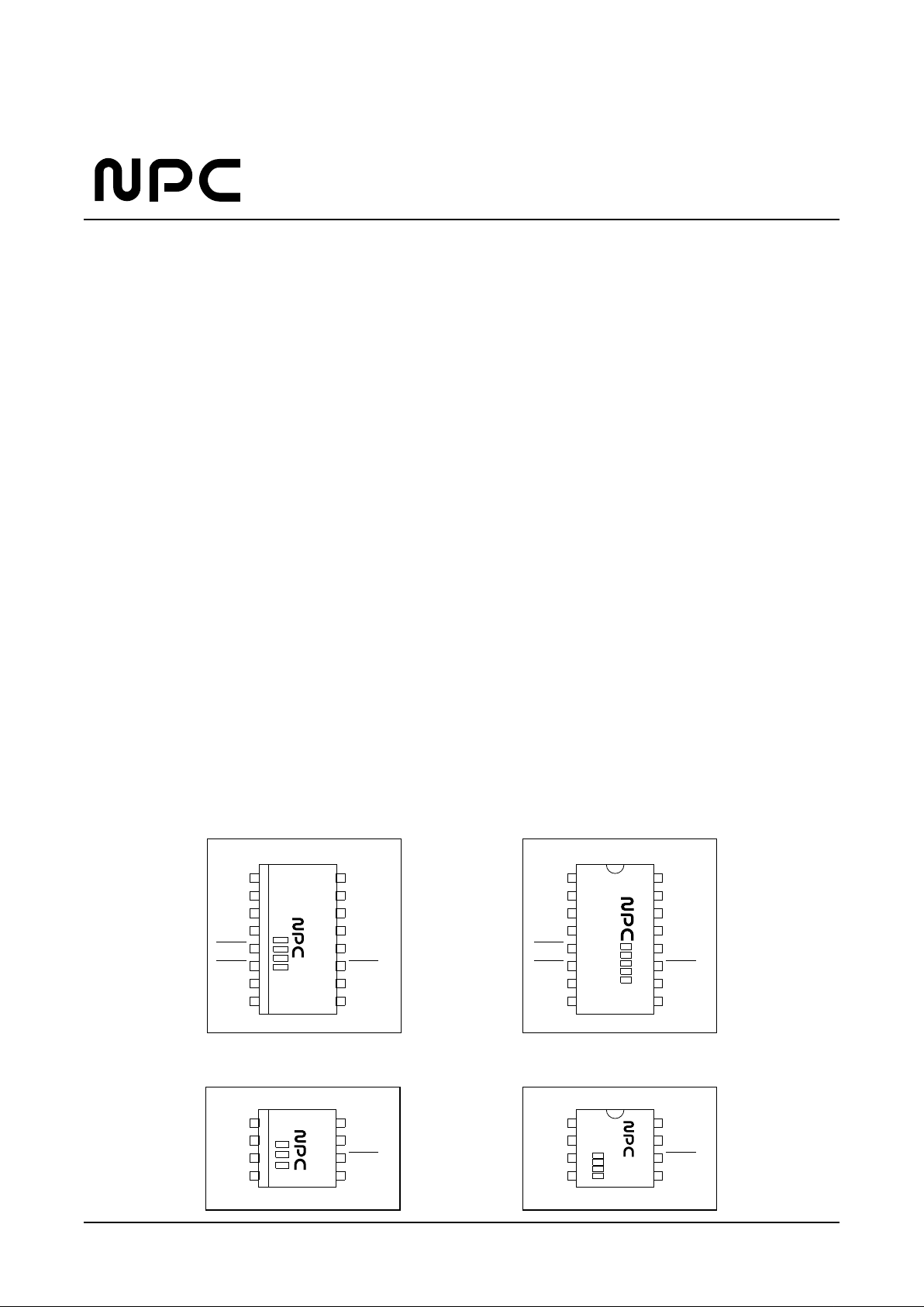
•Package
SM8220: 16 pin SOP, 16 pin DIP
SM8221: 8 pin SOP, 8 pin DIP
APPLICATIONS
•Calling Number Delivery service
•Adjunct Boxes
•Telephone Answering Machines
•Feature Phones
•Fax Machines
•Computer Interface Products
PINOUT
(Top View)
8
220
1
9
16
8
TIP
RING
AGND
RDIN
RDRC
RDET
PDWN
VDD
FOUT
DMIN
DOUT
NC
CDET
OSCOUT
GND
OSCIN
/CLKIN
1
9
16
8
SM8220S (16pin SOP) SM8220P (16pin DIP)
S
M
8
220
S
MS
P
1
4
5
8
TIP
RING
PDWN
GND
VDD
DOUT
CDET
CLKIN
1
4
5
8
SM8221S (8pin SOP) SM8221P (8pin DIP)
8
221
S
M
P
TIP
RING
AGND
RDIN
RDRC
RDET
PDWN
VDD
FOUT
DMIN
DOUT
NC
CDET
OSCOUT
GND
OSCIN
/CLKIN
TIP
RING
PDWN
GND
VDD
DOUT
CDET
CLKIN
8
221
Page 2
NIPPON PRECISION CIRCUITS-2
SM8220/SM8221
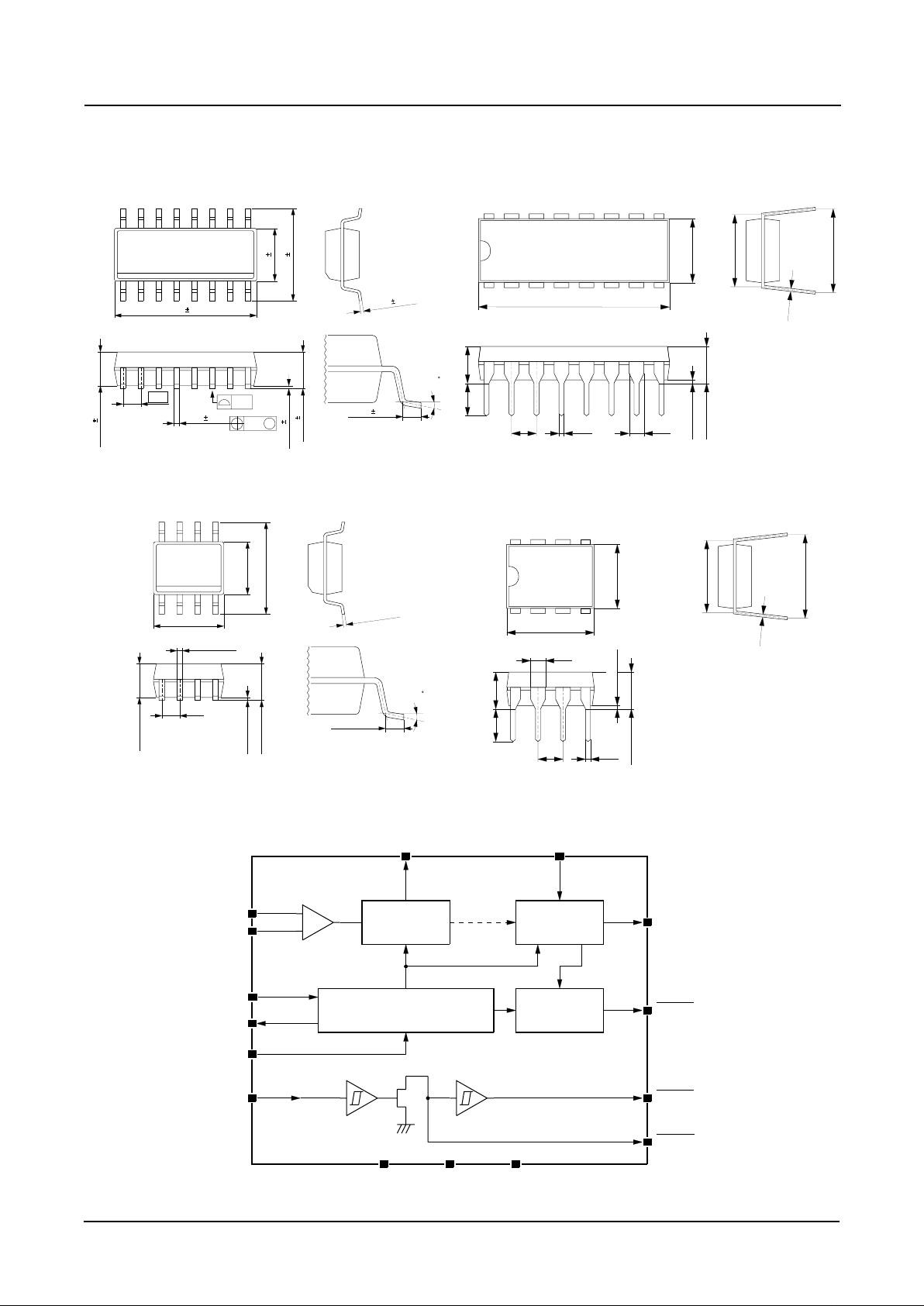
PACKAGE DIMENSIONS
(Unit: mm)
TIP
RING
OSCIN*
/CLKIN
OSCOUT*
PDWN
RDIN*
FOUT* DMIN*
DOUT
CDET
RDET*
Band Pass
Filter
FSK
Demodulator
Power Down Control
and Clock Generator
Carrier
Detect
(SM8221)
AGND* VDD
GND
*: Not available for SM8221.
RDRC*
BLOCK DIAGRAM
19.05
2.54
0.25
2.54 0.46 1.52
3.68 to 4.32
0.38 to 1.02
6.35
3.18 3.30
7.49 to 8.13
8.13 to 9.40
0 to 8
9.89 0.09
6.00 0.20
3.90 0.09
1.375 0.275
1.27
0.25
0.41 0.05
0.10
1.55 0.20
0.175 0.075
M
0.13 0.06
0.84 0.43
SM8220S (16 pin SOP) SM8220P (16 pin DIP)
SM8221S (8 pin SOP) SM8221P (8 pin DIP)
8.89
2.54
0.25
2.54 0.46
1.52
3.68 to 4.32
0.38 to 1.02
6.35
3.18 3.30
7.49 to 8.13
8.13 to 9.40
1.27
0.10 to 0.25
4.80 to 4.98
3.81 to 3.99
0.36 to 0.46
0.19 to 0.25
1.35 to 1.75
1.10 to 1.65
0.41 to 1.27
0 to 8
5.80 to 6.20
Page 3

NIPPON PRECISION CIRCUITS-3
SM8220/SM8221
PIN DESCRIPTIONS
Number Name i/o Function
SM8220 SM8221
1 1 TIP i
2 2 RING i
3 - AGND o
4 - RDIN si
5 - RDRC od
6 - RDET o
7 3 PDWN si
8 4 GND 9 5 OSCIN i
/CLKIN
10 - OSCOUT o
11 6 CDET o
12 - NC 13 7 DOUT o
14 - DMIN i
15 - FOUT o
16 8 VDD -
(Note) si: Schmitt Triger Input, od: Open Drain Output.
Tip Input: This pin is connected to the tip side of the twisted pair telephone wires.
This pin must be DC isolated from the phone line.
Ring Input: This pin is connected to the ring side of the twisted pair telephone wires.
This pin must be DC isolated from the phone line.
Analog Ground: 1/2 V
DD voltage output. This pin must be grounded through 0.1 µF capacitor.
Ring Detect Input: The attenuated ring signal is connected to this pin for the ring detection.
Ring Detect RC Terminal: An RC network will be connected to this pin to set time delays for
the ring signal detection.
Ring Detect Output: This pin is an output of a schmitt trigger buffer which input is connected
to RDRC pin. The low level at this pin indicates that the ring signal is detected.
Power Down Control: This pin must be kept at low level for the normal operation.
When it is high, the device will be in the power down.
Under the power down mode, OSCOUT, CDET and DOUT pins are set to high level and
AGND, FOUT pins are set to high impedance.
Device Ground: This pin is connected to the system ground.
Crystal Oscillator Input: A crystal will be connected between this pin and OSCOUT pin.
This pin may be driven from an external clock source.
Crystal Oscillator Output: A crystal will be connected between this pin and OSCIN pin.
This pin must be kept open when OSCIN pin is driven from an external clock source.
Carrier Detect Output: When low, this output indicates that a valid carrier present on the line.
No connection pin.
Data Out: This pin presents the output of the demodulator while CDET pin is low.
When CDET pin goes high, this pin is held high.
Demodulator Input: This pin is connected from FOUT pin through a 0.1µF capacitor.
No other components should be connected to this pin.
Band Pass Filter Output: This pin is connected to DMIN pin through a 0.1µF capacitor.
No other components should be connected to this pin.
Power Supply: Positive power supply pin.
Page 4

NIPPON PRECISION CIRCUITS-4
SM8220/SM8221
ABSOLUTE MAXIMUM RATINGS
Parameter Symbol Condition Rating Unit
Supply Voltage V
DD −0.5 to 7.0 V
Input Voltage V
IN −0.3 to VDD+0.3 V
Input Current I
IN ±10 mA
Power Dissipation P
D 120 mW
Operating Temperature Range Ta −20 to 85 °C
Storage Temperature Range TSTG −40 to 125 °C
Soldering Temperature T
SLD 255 °C
Soldering Time
tSLD 10 sec
(GND= 0V unless otherwise noted)
ELECTRICAL CHARACTERISTICS
DC CHARACTERISTICS
Rating
Parameter Symbol Condition MIN TYP MAX Unit
DC Supply Voltage V
DD 3 5 5.5 V
Supply Current I
DD *1 1.7 3 mA
Power Down Current I
DPD *2 1 µA
Input Low Voltage1 V
IL1 OSCIN/CLKIN pin 0.3VDD V
V
OSCOUT= 0.8VDD
Input High Voltage1 VIH1 OSCIN/CLKIN pin 0.7VDD V
V
OSCOUT= 0.2VDD
Input Low Voltage2 VIL2 PDWN, RDIN, RDRC pin 2 0.3VDD V
Input High Voltage2 V
IH2 PDWN, RDIN, RDRC pin 0.75VDD 3V
Output Low Voltage V
OL DOUT, RDET, CDET, RDRC 0.4 V
pin, V
DD= 4.5V, IOL= 1.6mA
Output High Voltage V
OH DOUT, RDET, CDET pin 3.7 V
V
DD= 4.5V, IOH= −1.6mA
Input Leakage Current I
IN OSCIN/CLKIN, PDWN, RDIN −11µA
pin, V
DD= 5.5V, VIN= 0 or 5V
Output Leakage Current I
OFF RDRC pin, RDIN= 0V 1 µA
V
DD= 5.5V,VOH= 5.5V
Input DC Resistance R
IN TIP, RING pin, VDD= 5V 175 250 325 kΩ
Impedance measured from 1/2V
DD
(VDD= 5±0.5 V, GND = 0 V, fCLK = 3.579545 MHz, Ta = −20 to 85 ˚C unless otherwise noted)
*1: OSCIN/CLKIN= 0V, PDWN= 0V, RDIN= 0V, RDRC= 0V, Other Input Pins= open
*2: OSCIN/CLKIN= 0V, PDWN= V
DD, RDIN= 0V, RDRC= 0V, Other Input Pins= open
Page 5

NIPPON PRECISION CIRCUITS-5
SM8220/SM8221
AC CHARACTERISTICS
Rating
Parameter Symbol Condition MIN TYP MAX Unit
Input Sensitivity TIP, RING pin −48 dBm
TIP, RING pin V
DD= 5V −15 dBm
Input Level V
DD= 3V −18
Band Pass Filter Frequency Response 60Hz −80 dB
(relative to 1700 Hz @ −34 dBm 1200 Hz −1
input level) 2200Hz 0
4000Hz −43
≥10000Hz −54
Carrier Detect ON Sensitivity CD
ON CDET pin −48 −44 dBm
Carrier Detect OFF Sensitivity CD
OFF CDET pin −55 −51 dBm
Oscillator Frequency f
CLK −0.1% 3.579545 +0.1% MHz
(VDD= 5.0V, GND= 0V, fCLK= 3.579545MHz, Ta= −20 to 85 ˚C, 0dBm= 0.7746Vrms @ 600Ω unless otherwise noted)
TYPICAL BAND-PASS FILTER FREQUENCY RESPONSE
(Relative to 1700 Hz @ −34 dBm input level)
-100
-80
-60
-40
-20
0
20
0 1000 2000 3000 4000
Frequency (Hz)
Gain (dB)
SWITCHING CHARACTERISTICS
Rating
Parameter Symbol Condition MIN TYP MAX Unit
Power Down Low to
tDOSC 5ms
Oscillator Start Up
Power Down Low to
tSUPD 10 ms
FSK Data Detect
Carrier Detect Acquisition Time
tDAQ 10 ms
End of Data to Carrier Detect High
tDCH 10 ms
(VDD= 5.0V, GND= 0V, fCLK= 3.579545MHz, Ta= 25 ˚C, CL= 50pF unless otherwise noted)
Page 6

NIPPON PRECISION CIRCUITS-6
SM8220/SM8221
FUNCTIONAL DESCRIPTION
Bell 202 ITU-T V.23
Modulation Type Continuous - phase binary frequency shift keying (FSK)
Logical 1 (Mark) 1200 ± 12Hz 1300 ± 22Hz
Logical 0 (Space) 2200 ± 22Hz 2100 ± 22Hz
Carrier Frequency 1700Hz 1700Hz
Transmission rate 1200BPS 1200BPS
Data format serial, asynchronous serial, asynchronous
The SM8220/SM8221 Calling Number Identification
Receiver IC is a device compatible with the Bellcore GR30-CORE for transmitting asynchronous voice-band data
to Customer Premises Equipment (CPE) from a serving
Stored Program Controlled Switching System (SPCS) or a
Central Office (CO). This data transmission technique is
applicable in a variety of services such as Calling Number
Delivery (CND), Calling Name Delivery (CNAM). With
these services, a subscriber will have the ability to display a
message containing the phone number of the calling party,
the name of a calling party, the date and the time.
The data signaling interface should conform to Bell 202 and ITU-T V.23 specification, which is:
101010... 1 Data
1st Ring 2nd Ring
Channel
Seizure
Signal
Mark
Signal
*
Message
Type
Word
Message
Length
Word
Message
Words
*
Checksum
Word
*
*: Mark bits
Single
Message
Format
101010... 1 Data
1st Ring 2nd Ring
Channel
Seizure
Signal
Mark
Signal
*
Message
Type
Word
Message
Length
Word
*
Multi
Message
Format
*
Parameter
Type
Word
Parameter
Length
Word
*
Parameter
Words
Checksum
Word
*
Parameter
Type
Word
Parameter
Length
Word
* *
*
*
Parameter
Type
Word
Parameter
Length
Word
* *
Parameter
Words
Parameter
Words
*: Mark bits
Bellcore GR-30-CORE Data Format
Page 7

NIPPON PRECISION CIRCUITS-7
SM8220/SM8221
TIMING DIAGRAM
TYPICAL APPLICATION CIRCUIT
101010... 1 Data
1st Ring 2nd Ring
101010... 1 Data
INPUT
(TIP, RING)
PDWN
DOUT
OSCOUT*
RDRC*
RDET*
CDET
*: Not available for SM8221.
V
IH2
VIL2
tSUPD
tDAQ tDCH
tDOSC
Protection
Network
TIP
RING
AGND
RDIN
RDRC
RDET
PDWN
GND
VDD
DOUT
NC
DMIN
FOUT
CDET
OSCOUT
OSCIN
/CLKIN
SM8220
Controller
From TIP
From RING
0.001µF
91kΩ (240kΩ)
0.2µF
0.2µF
0.001µF 91kΩ (240kΩ)
0.1µF
470kΩ
33kΩ
270kΩ
0.2µF
10µF
0.1µF
+5V
LCD Driver
LCD Display
3.579545
MHz
( ) = When 3V range
Protection
Network
TIP
RING
PDWN
GND
VDD
DOUT
CLKIN
SM8221
Controller
From TIP
From RING
0.001µF 91kΩ (240kΩ)
0.001µF
91kΩ (240kΩ)
10µF
+5V
LCD Driver
LCD Display
CDET
3.579545MHz
( ) = When 3V range
(Note)
When the Ring Detect feature of SM8220 is not used, always connect RDIN and RDRC pins to the system ground level.
This will cut excess current drain from VDD under the normal and power down mode of operation.
This diagram example is desingned to adapt to the specifications of United States.
When it is used in other area, the constants may have to chenged appropriately.
Page 8

NIPPON PRECISION CIRCUITS-8
SM8220/SM8221
NIPPON PRECISION CIRCUITS INC. reserves the right to make changes to the products described in this data sheet in order to
improve the design or performance and to supply the best possible products. Nippon Precision Circuits Inc. assumes no responsibility for
the use of any circuits shown in this data sheet, conveys no license under any patent or other rights, and makes no claim that the circuits
are free from patent infringement. Applications for any devices shown in this data sheet are for illustration only and Nippon Precision
Circuits Inc. makes no claim or warranty that such applications will be suitable for the use specified without further testing or modification. The products described in this data sheet are not intended to use for the apparatus which influence human lives due to the failure or
malfunction of the products. Customers are requested to comply with applicable laws and regulations in effect now and hereinafter, including compliance with export controls on the distribution or dissemination of the products. Customers shall not export, directly or indirectly, any products without first obtaining required licenses and approvals from appropriate government agencies.
NIPPON PRECISION CIRCUITS INC.
4-3, FUKUZUMI 2 CHOME, KOTO-KU
TOKYO,135-8430 JAPAN
Telephon: +81-3-3642-6661
Facsimile: +81-3-3642-6698
NC9508DE 1998. 7
NIPPON PRECISION CIRCUITS INC.
 Loading...