

Page 1
SM8213AM
NIPPON PRECISION CIRCUITS INC.
POCSAG Decoder For Multiframe Pagers
OVERVIEW
The SM8213AM is a POCSAG-standard (Post
Office Code Standardization Advisory Group) signal
processor LSI, which conforms to CCIR recommendation 584 concerning standard international wireless calling codes.
The SM8213AM supports call messages in either
tone, numerical or character outputs at signal speeds
of 512, 1200 or 2400 bps. The signal input stage features a built-in filter.
Each of the addresses (max. 7 + 1 dummy = 8) can
be assigned to any frame, which also makes the
device configurable for many additional services.
Each address can be independently set to ON/OFF.
Furthermore, built-in buffer memory means decoded
information can be fetched in sync with the microcontroller clock, thereby reducing the microcontroller CPU time required. Intermittent-duty method
(battery saving (BS) method) control signals, compatible with PLL operation, and Molybdenum-gate
CMOS structure makes possible the construction of
low-voltage operation, low power dissipation systems.
25 to 75% duty factor signal coverage
■
8 rate error detection condition settings
■
76.8 kHz system clock (crystal oscillator)
■
76.8 or 38.4 kHz clock output pin
■
Built-in oscillator capacitor and feedback resistor
■
2.0 to 3.5 V operating supply voltage
■
Molybdenum-gate CMOS process realizes low
■
power dissipation
16-pin SSOP
■
PINOUT
T op V iew
BS1
BS2
BS3
SIGNAL
XT
XTN
1
8
16
8213AM
VDD
ATTN
SDI
SDO
SCKXVSS
AREA
RSTN
9
CLKOVSS
The SM8213AM is available in 16-pin SSOPs.
FEATURES
Conforms to POCSAG standard for pagers
■
512, 1200 or 2400 bps signal speed
■
Multiframe compatible (each address individually
■
controllable)
8 addresses × 4 sub-addresses (total of 32
■
addresses) control
(8 addresses comprise 7 actual addresses + 1
dummy address)
Built-in buffer memory (1 code word)
■
Supports tone, numeric or character call messages
■
Built-in input signal filter, with filter ON/OFF and
■
4 selectable filter characteristics
PLL-compatible battery saving method (BS1,
■
BS2, BS3 outputs)
BS1 (RF control main output signal) 61-step setup
■
time setting
BS3 (PLL setup signal) 61-step setup time setting
■
BS2 (RF DC-level adjustment signal) before/dur-
■
ing reception selectable adjustment timing
1-bit and 2-bit burst error auto-correction function
■
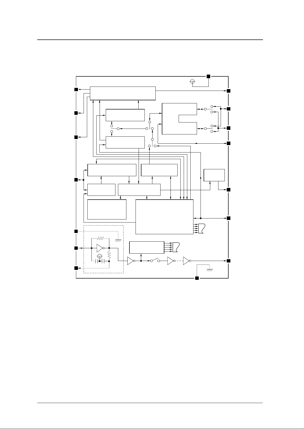
PACKAGE DIMENSIONS
Unit: mm
4.4 0.2
6.2 0.3
0.6TYP
6.8 0.3
0.80.36 0.1
1.5 0.1
0.05 0.05
010
0.15
+ 0.10
- 0.05
0.4 0.2
NIPPON PRECISION CIRCUITS—1
Page 2
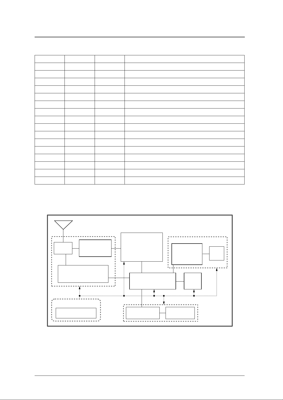
BLOCK DIAGRAM
SM8213AM
VDD
BS1
BS2
BS3
SIGNAL
XVSS
Timing Control
Flag Register
Address Register
Receive Data Register
Digital PLL
Preamble Pattern
Sync Code
Idle Code
Data Comparator
Buffer Register
(Ring)
Buffer Register
Error Correction
Main Control
Circuit
ATTN
SDI
SDO
SCK
Timer
AREA
RSTN
Each Switch
and Register
XT
XTN
Clock Control
Each Working Block
CLKO
VSS
NIPPON PRECISION CIRCUITS—2
Page 3
PIN DESCRIPTION
SM8213AM
Number Name I/O
1 BS1 O RF control main output signal
2 BS2 O RF DC-level adjustment signal
3 BS3 O PLL setup signal
4 SIGNAL I NRZ signal input pin
5 XVSS – Crystal oscillator ground. Capacitor connected between XVSS and VDD
6 XT I Oscillator input pin
7 XTN O Oscillator output pin
8 VSS – Ground
9 CLKO O 76.8 or 38.4 kHz clock output
10 RSTN I Hardware clear (reset)
11 AREA O Sync code detection output (HIGH for minimum 1 sec. on detection)
12 SCK I CPU-to-decoder data transfer sync clock
13 SDO O Status and received data output to CPU
14 SDI I Data input from CPU (including ID data)
15 ATTN O Interrupt detect signal output pin (Ready for data transmission when LOW)
16 VDD – Supply voltage
1. I = input, O = output
1
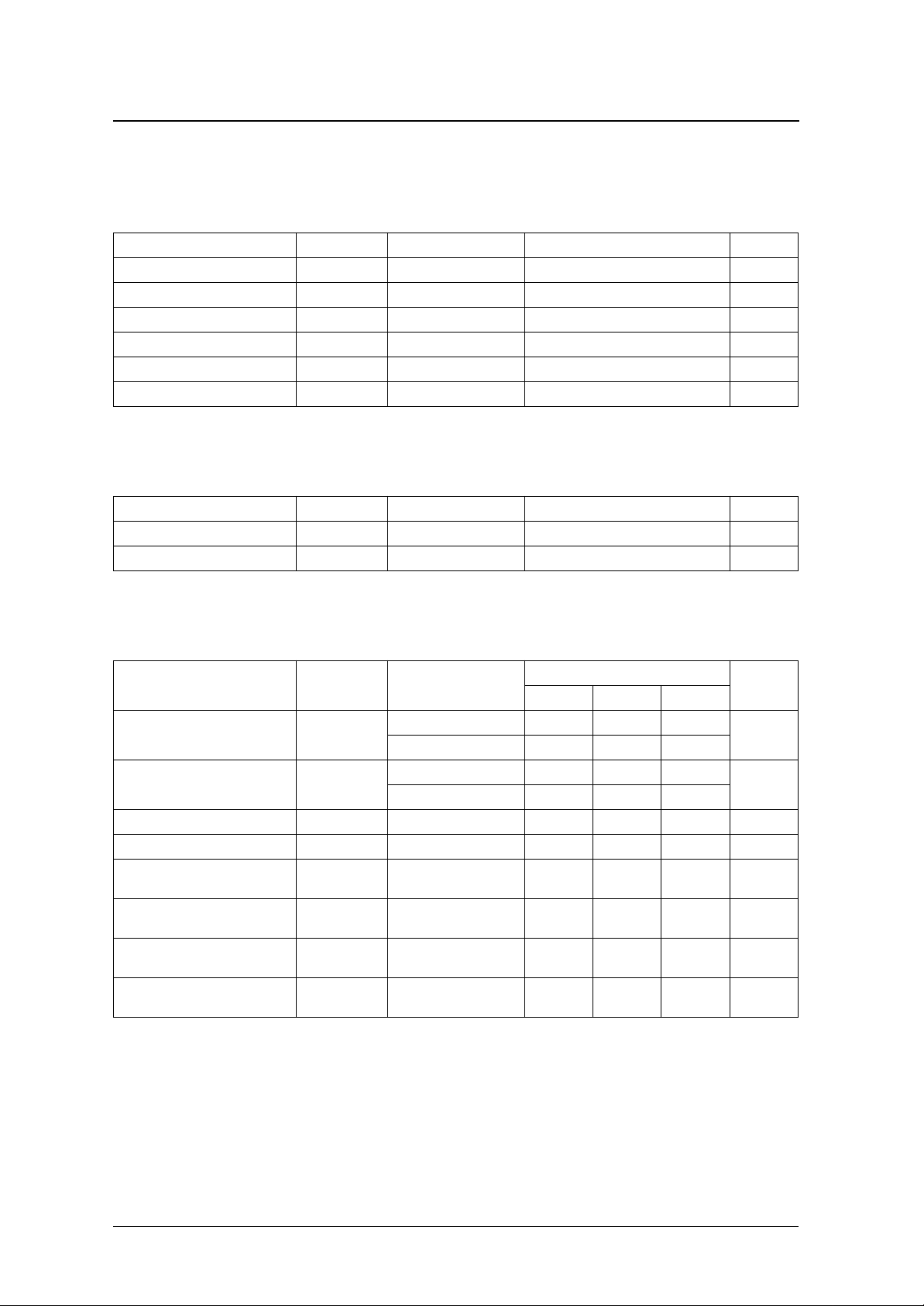
Description
SM8213AM Paging Receiver Block Diagram
POCSAG
RF
Waveform
Recovery
Decoder
SM8213
PLL Circuit
CPU Unit
Supply Unit
D/D Converter LCD Driver
Alert
Melody
SP
IC
ID
ROM
LCD
NIPPON PRECISION CIRCUITS—3
Page 4
SPECIFICATIONS
Absolute Maximum Ratings
V
= 0 V
SS
Parameter Symbol Condition Rating Unit
Supply voltage range V
Input voltage range V
Power dissipation P
Storage temperature range T
Soldering temperature T
Soldering time t
Recommended Operating Conditions
DD
IN
D
stg
sld
sld
SM8213AM
−
0.3 to 7.0 V
−
V
0.3 to V
SS
+ 0.3 V
DD
250 mW
−
40 to 125
255
° C
° C
10 s
V
= 0 V
SS
Parameter Symbol Condition Rating Unit
Supply voltage range V
Operating temperature range T
DD
opr
DC Characteristics
Recommended operating conditions unless otherwise noted
Parameter Symbol Condition
V
= 3.0 V – 3.0 6.0
Operating current consumption
(IDLE mode)
Standby supply current
1
2
HIGH-level input voltage (all inputs) V
LOW-level input voltage (all inputs) V
HIGH-level output current
(all outputs except XTN)
LOW-level output current
(all outputs except XTN)
HIGH-level output current
(all outputs except XTN)
LOW-level output current
(all outputs except XTN)
I
I
DD1
DD2
I
OH
I
OL
I
OH
I
OL
IH
IL
DD
V
= 2.0 V – 2.0 4.0
DD
V
= 3.0 V – 3.0 6.0
DD
V
= 2.0 V – 2.0 4.0
DD
V
OH
V
OL
V
OH
V
OL
= 2.6 V, V
= 0.4 V, V
= 1.6 V, V
= 0.4 V, V
= 3.0 V 0.6 1.4 – mA
DD
= 3.0 V 1.0 2.2 – mA
DD
= 2.0 V 0.3 0.7 – mA
DD
= 2.0 V 0.7 1.5 – mA
DD
2.0 to 3.5 V
−
20 to 70
Rating
min typ max
0.8V
DD
––V
– – 0.2V
° C
Unit
µA
µA
DD
V
1. CLKO output is inactive. The consumption current is slightly higher when RSTN is going LOW.
2. Oscillator circuit is working.
NIPPON PRECISION CIRCUITS—4
Page 5
SM8213AM
AC Characteristics
Recommended operating conditions unless otherwise noted
Parameter Symbol Condition
XT clock frequency f
XT clock duty cycle D
SCK clock pulsewidth t
SCK clock interval
(except WRITE mode)
SCK clock interval (WRITE mode) t
SDI data setup time t
SDI data hold time t
SDO data setup time t
SDO data hold time t
ATTN data setup time t
ATTN data hold time t
CLKO clock rise time t
CLKO clock fall time t
CLKO clock delay time D
RSTN pulsewidth t
CYXT
XT
PWSC
t
CYSC
CYSC
SSDI
HSDI
SSDO
HSDO
SATT
HATT
RCLK
FCLK
CLKO
PWRS
512 bps 5 – 1900
2400 bps 5 – 415
No load – – 500 ns
No load – – 500 ns
Rating
min typ max
−
250 ppm 76.8 +250 ppm kHz
Unit
25–75%
2 – 150 µs
µs1200 bps 5 – 830
5 – 830 µs
1––µs
1––µs
3––µs
––0µs
0––µs
1––µs
––1µs
1––ms
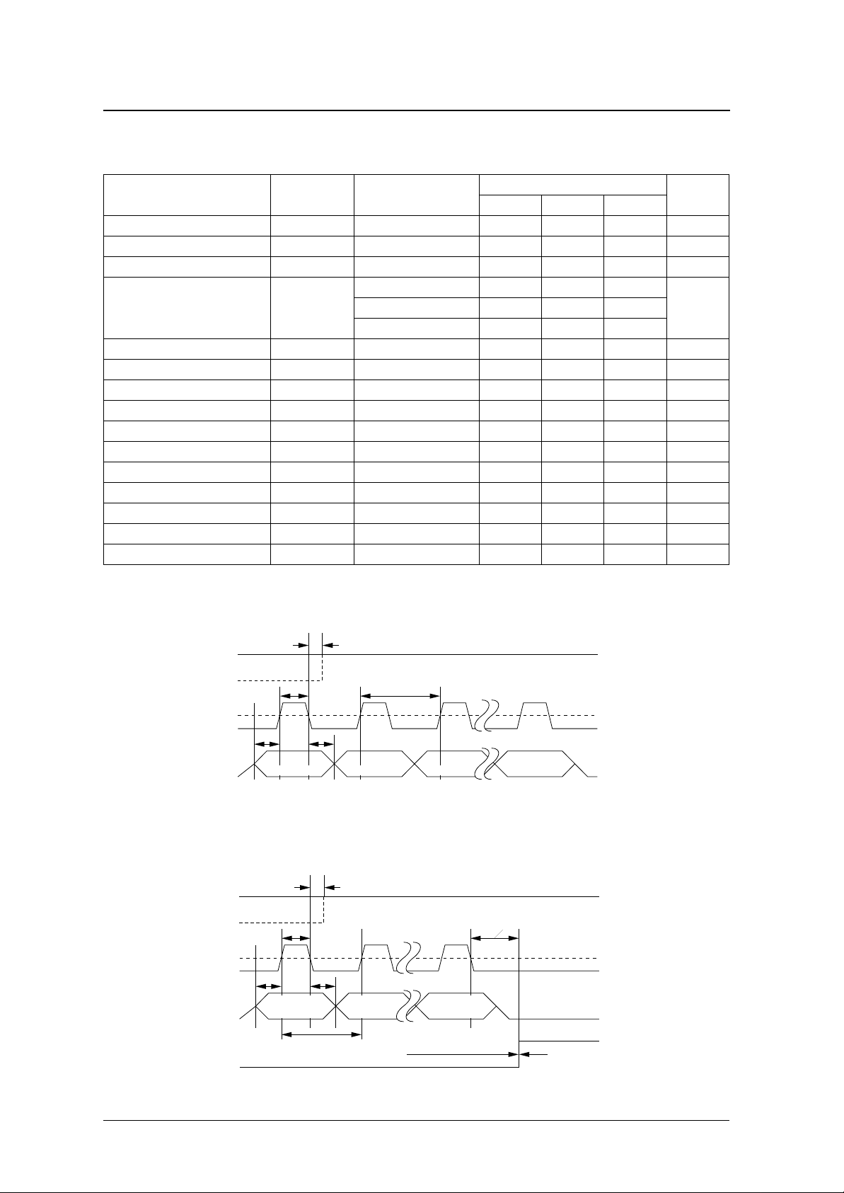
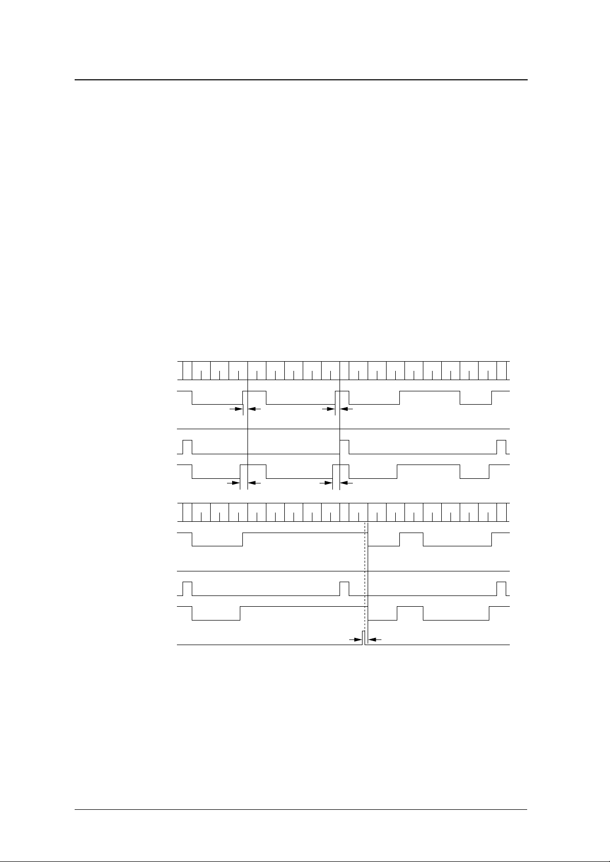
Parameter/address set timing
tHATT
ATTN
tPWSC
SCK
12332
tSSDI tHSDI
SDI
INPUT
DATA 1
Auxiliary operating mode set timing
tHATT
ATTN
tPWSC
SCK
SDI
128
Decoder
Setting1
tCYSC
1/ 2*VDD
INPUT
DATA 2
INPUT
DATA 3
START command : 66 bit time max
Others : 2 bit time max
INPUT
DATA 32
1/ 2*VDD
tHSDItSSDI
Decoder
Setting 2
Decoder
Setting 8
Decoder Mode
tCYSC
Next ModeCurrent Mode
NIPPON PRECISION CIRCUITS—5
Page 6
Status data read timing
ATTN
tPWSC
SCK
1289
tHSDItSSDI
SDI
READ
COMMAND 1
tCYSC
SDO
Don't
Care 1
Received data transfer timing
READ
COMMAND 2
Don't
Care 2
SM8213AM
READ
COMMAND 8
Don't
Care 8
COMMAND 9
STATUS
DATA 1
tSSDO
READ
tHSDO
15 16
READ
COMMAND 15
STATUS
DATA 7
READ
COMMAND 16
STATUS
DATA 8
1/ 2*VDD
ATTN
tSATT
SCK
SDI
tSSDO tHSDO
SDO
CLKO clock output timing
(XT)
(76.8kHz)
CLKO
(76.8kHz Mode)
OUTPUT
DATA 1
tHATT
tPWSC
12332
OUTPUT
DATA 2
tCYSC
DCLKO
OUTPUT
DATA 3
OUTPUT
DATA 32
αβ
α
XT =
D
α+β
tRCLKtFCLK
1/ 2*VDD
0.7*VDD
1/ 2*VDD
0.3*VDD
0.7*VDD
1/ 2*VDD
0.3*VDD
0.7*VDD
CLKO
(38.4kHz Mode)
1/ 2*VDD
tRCLKtFCLK
NIPPON PRECISION CIRCUITS—6
0.3*VDD
Page 7
FUNCTIONAL DESCRIPTION
SM8213AM
Unless otherwise specified, values in diagrams without parentheses are for 512 bps, in ( ) are for 1200
value of PL5 (MSB) to PL0 (LSB), and “N” represents the value of RF5 (MSB) to RF0 (LSB).
bps, and in [ ] are for 2400 bps. “M” represents the
Receive Format
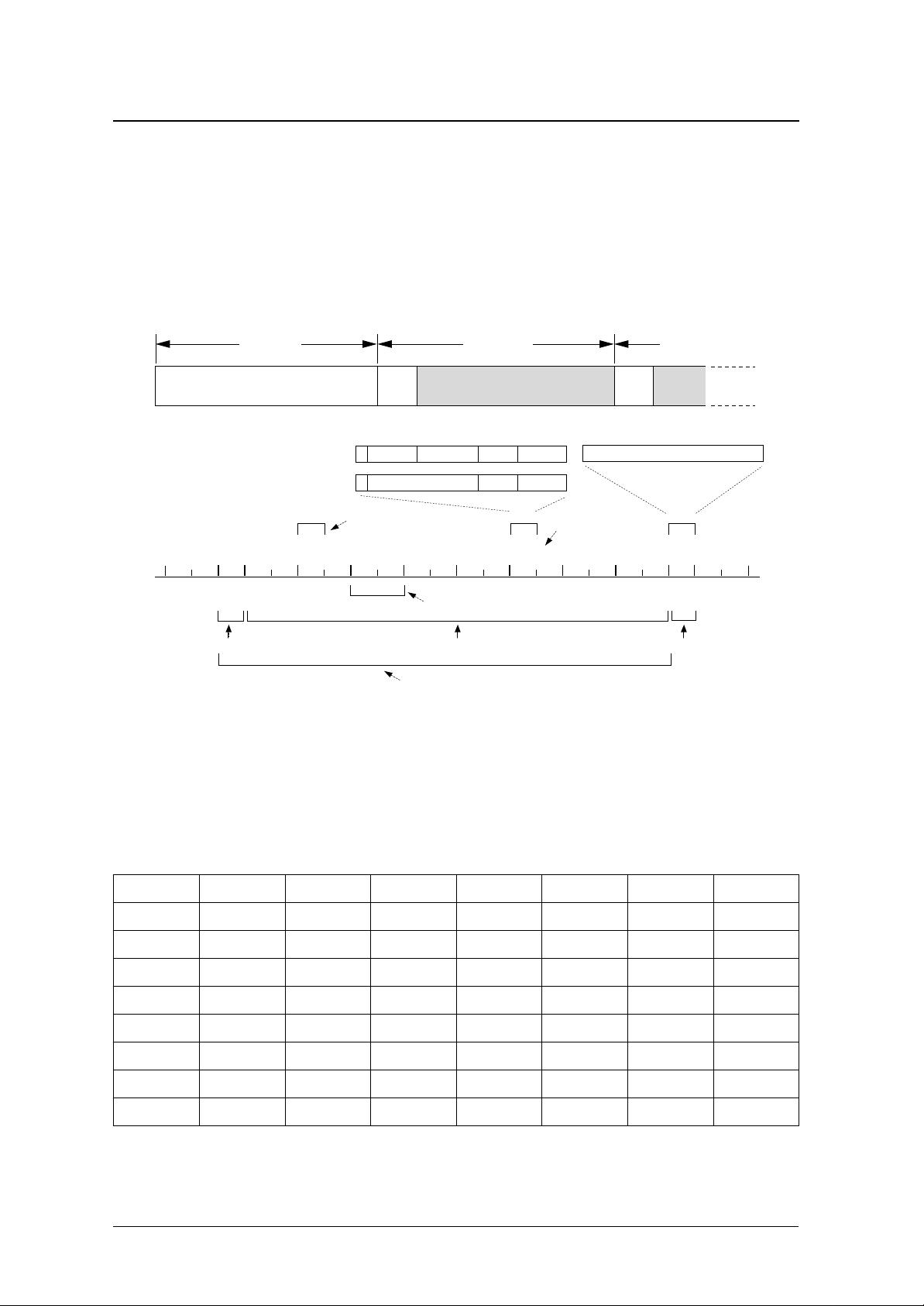
The receive format conforms to CCIR RPC No. 1 (POCSAG).
Preamble 1st Batch 2nd Batch
Continuous 575 - bit "1, 0" bit pattern
Address signal
Message signal
7
SC
01
Sync
Code
12
0
1
19 20 21 22 31
Address bits Function bits Check bits
Message bits
1 Code Word
234
1 Frame(= 2 Code Words)
Check bits
Sync
Code
32
Even - parity bit
Even - parity bit
1
Sync Code Word
Frame No.
567
SC
32
0
Sync Code Part
Frame Part
Sync Code Part
1 Batch
Figure 1. Receive signal format
Sync signal (SC)
The sync signal is a continuous code word in the
received signal, used for word synchronization. It
even-parity bit, making a 32-bit signal. The sync
code word pattern is shown in table 1.
comprises 31 bits in an M-series bit pattern plus one
Table 1. Sync code format
Bit number Bit value Bit number Bit value Bit number Bit value Bit number Bit value
1091170251
2 1101180261
3 1110190270
4 1121201281
5 1130210291
6 1140221300
7 0151230310
8 0160241320
NIPPON PRECISION CIRCUITS—7
Page 8
SM8213AM
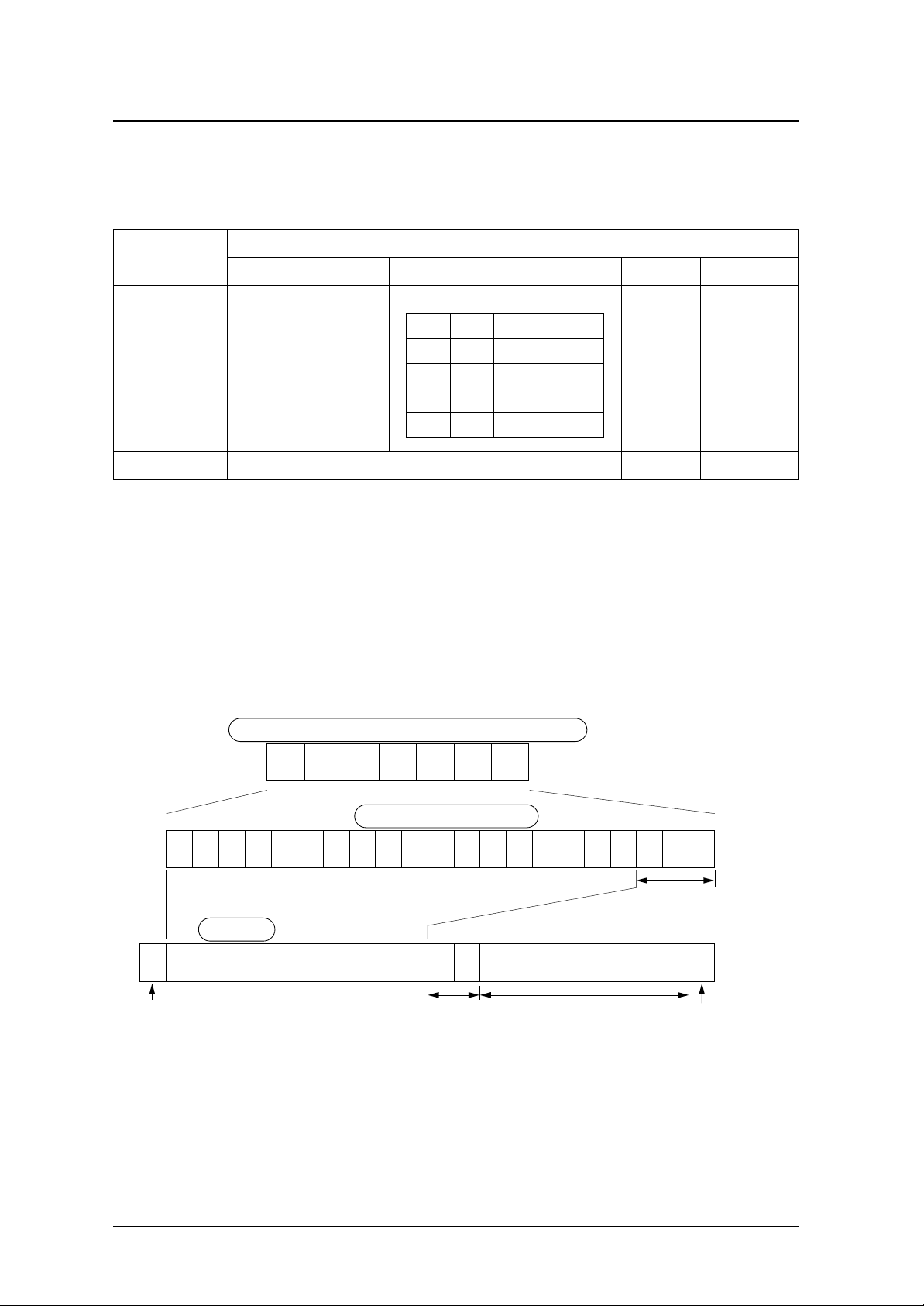
Code words (address and message signals)
Each code word comprises 32 bits as shown in table 2.
Table 2. Code word format
Code word
Address signal 0 Address bits
Message signal 1 Message bits Check bits Even-parity bit
1. The MSB is the address/message code word control bit. It is 0 for an address signal, and 1 for a message signal.
2. Bits 2 to 21 contain the address or message information.
3. Bits 22 to 31 are BCH(31,21) format generated check bits, where BCH(n,k) = BCH(word length, number of information bits).
4. The LSB is an even-parity bit for bits 1 to 31.
1 (MSB)
1
2 to 19
2
Function bits
20 21 Function
0 0 A call
0 1 B call
1 0 C call
1 1 D call
Bit number
2
20, 21
3
22 to 31
Check bits Even-parity bit
32 (LSB)
Call number to call sign conversion
This conversion expands a 7-digit decimal call number into a 21-bit binary call sign, as shown in figure
2.
After expansion, the high-order 18 bits are assigned
to bits 2 to 19 (address signal), and the low-order 3
bits are the user-defined frame identification pattern,
which is stored in ID-ROM. The two function bits
define which of four call functions is active.
4
7 - digit decimal call signal (gap code) (8 to 2000000)
1234567
MSB LSB
21 - bit binary conversion
123456789101112131415161718192021
identification
1 2 19 20 21 323122
0
Flag : "0" = Adderss signal
Call sign
Bits 2 to 19 (18 bits)
Function bits
Bits 22 to 31 (10 bits)
BCH(31, 21) generated check bits
Figure 2. Call number to call sign conversion
Frame
pattern
P
Even - parity bit
(for bits 1 to 31)
NIPPON PRECISION CIRCUITS—8
Page 9
Idle signal
SM8213AM
In the POCSAG format, for pager systems that send
numeric data, the message information content varies and as a result an idle signal or another address
signal is inserted after the message to indicate the
end of the message.
That is, if no address word or message word exists
for a frame within a batch or for a code word within
a frame, the idle pattern, shown in table 3, is trans-
Table 3. Idle code format
Bit number Bit value Bit number Bit value Bit number Bit value Bit number Bit value
1091171251
2 1100181260
3 1110190270
4 1120200281
5 1131210290
6 0140220301
7 1150230311
8 0161241321
mitted in its place. Then during message signal
reception, the message ends when the idle signal is
detected.
The SM8213AM supports 2 methods of determining
the end of message. Namely, a message ends when
either an idle signal or another address is received
(POCSAG format), or when an interrupt signal from
the CPU is received.
Receive signal duty factor
During preamble detection, the preamble pattern
(1,0) is recognized at duty factors from 25% (min) to
75% (max) of the (1,0) preamble cycle.
Error correction and detection
The SM8213AM performs error correction (or
detection) on each code word as described in table 4.
Table 4. Error correction
Item Description
Preamble Pattern Detection Selectable 1 to 8 rate errors in 6 to 544 bits
Synchronization Code word Detection 2 random errors in 32 bits
Self Address Code word Detection 2 random errors in 32 bits
Message Code word 1-bit and 2-bit burst errors in 31 bits
An error is deemed to have occurred when 2 or more
signal edges occur within 1-bit unit time, and a rate
error is deemed to have occurred when the number of
Note that there are 8 selectable error correction conditions for the preamble pattern.
errors exceeds the counter value. Refer to the “Preamble Mode” section for a discussion of the error
counter.
NIPPON PRECISION CIRCUITS—9
Page 10
Battery Saving (BS1, BS2, BS3)
SM8213AM
The SM8213AM controls the intermittent-duty operation of the RF stage, which reduces battery consumption, and three output control signals (BS1,
BS2, BS3). The function each signal controls in each
mode is described below.
■
BS1 (RF-control main output signal)—The RF
stage is active when BS1 is HIGH. The risingedge setup time for receive timing is set by flags
RF0 to RF5 (61 steps). The maximum setup time
is 25.417 ms at 2400 bps, 50.833 ms at 1200 bps,
and 119.141 ms at 512 bps. Note that 3E
and
H
3FH are invalid settings for BS1.
■ BS2 (RF DC-level adjustment signal)—BS2 is
used to control the discharge of the receive signal
DC-cut capacitor. The function of BS2 is determined by flag BS2, as described below.
• When flag BS2 is 0, pin BS2 goes HIGH
together with BS1 and then goes LOW again
Receive code
BS1
01234567 01 345672
SYN
ICW
MES
ADD
ICW
MES
ICW
ADD
MES
MES
MES
Address does not match
after the BS1 setup time (idle mode). In preamble and lock mode (during address/message
reception), it stays LOW.
• When flag BS2 is 1, pin BS2 goes HIGH during
lock mode sync code receive timing and idle
mode signal receive timing. In preamble mode,
it stays LOW.
■ BS3 (PLL setup signal)—BS3 is used to control
PLL operation when the PLL is used. The risingedge setup time for receive timing is set by flags
PL0 to PL5 (61 steps). The maximum setup time
is 25.833 ms at 2400 bps, 51.667 ms at 1200 bps,
and 121.094 ms at 512 bps. Note that 3F
invalid setting for BS3.
Note that the setup times should be set up such that
(BS3 rising-edge setup time) > (BS1 rising-edge
setup time).
MES
ICW
ICW
ICW
ADD
MES
SYN
MES
MES
MES
MES
ICW
ICW
ADD
MES
MES
MES
MES
ICW
ADD
Self address
MES
ADD
is an
H
MES
SYN
BS2
(flag BS2 option = 0)
BS2
(flag BS2 option = 1)
BS3
Receive code
BS1
BS2
(flag BS2 option = 0)
BS2
(flag BS2 option = 1)
BS3
BREAK command
1.953*Nms (0.833*Nms)
[0.417*Nms]
1.953*Mms
(0.833*Mms) [0.417*Mms]
01234567 01 345672
SYN
MES
MES
ICW
ICW
ICW
ICW
ADD
Self address
1.953*Mms
(0.833*Mms) [0.417*Mms]
MES
MES
MES
MES
MES
MES
1.953*Nms (0.833*Nms)
[0.417*Nms]
MES
MES
MES
SYN
MES
MES
MES
ICW
ADD
MES
MES
BREAK detection to reception stop (32 bit max.)
Figure 3. BS1, BS2 and BS3 timing (Lock mode, frame 3)
MES
MES
ICW
ADD
MES
MES
ICW
ICW
ICW
SYN
NIPPON PRECISION CIRCUITS—10
Page 11

SM8213AM
Operating Modes
The SM8213AM has four operating modes—PowerON (Write), Preamble, Idle and Lock modes.
Power-ON mode
After power is applied, the internal registers should
be reset using RSTN.
When ATTN goes HIGH, the decoder sends a write
request for a decoder set read command and then
waits for the microcontroller (decoder set write command timing starts approximately 50 ms after reset,
but you should allow at least 900 ms for the oscillator internal to start and stabilize). The internal operation in write mode takes place at the same timing as
for 1200 bps speed mode.
Write data is prepared in 32-bit batches of 1 parameter batch and 8 address data batches for a total of 9
batches.
Ensure that there are not multiple writes requests to
turn ON the same address. Also, allow a minimum of
1.67 ms after transferring each command or data
before issuing the next processing command.
The parameter and address set commands are processed in sync with the decoder internal clock (1200
Hz). As a consequence, a gap of 28.4 ms minimum
RSTN
should be left between batches to provide time for
processing. Alternatively, data can be written by first
using the decoder set read command to confirm
whether or not processing is still in progress (BUSY)
before writing each batch. If the time gap is 28.4 ms
or greater, confirmation (READY) is not required.
After parameters and all addresses have been written
and after decoder processing, the decoder set start
command transfers operation from write mode and
starts preamble mode operation.
When setting parameters and addresses in write
mode, the SCK clock frequency should not be less
than 1200 Hz. If this occurs, the SCK counter is reinitialized. This function, however, does make restoring operation easy even if this or another clock is
accidentally input.
In write mode, after power is applied and after reset
initialization, all 9 batches (1 parameter and 8
address batches) should be set. If not all batches are
set, subsequent operation may become unstable.
SCK
SDI
SDO
BUSY
WRITE MODE
PREAMBLE MODE
1 ms min
READ
DAT A DAT A
READY
max.
1.67ms
max 900ms
: 8-bit unit time clock : 8-bit unit time indeterminate data
: 8-bit unit time data
DAT A : 32-bit unit time parameter/address data
Refer to the AC Characteristics section for detailed timing specifications.
READ
BUSY
max.
28.4ms
READY
Figure 4. Power-ON mode timing
STARTREAD
129ms max
129ms max
NIPPON PRECISION CIRCUITS—11
Page 12

Preamble mode
SM8213AM
Preamble mode is a continuous 544-bit long period.
If neither a preamble pattern, rate error nor sync code
is detected during this period, operation transfers to
idle mode.
If a preamble pattern is detected, the preamble mode
544-bit long period is recommenced.
If the sync code is detected, AREA goes HIGH and
operation transfers to lock mode. If an error of 2 bits
or less occurs, the detected word is recognized as the
Preamble Signal
Error bit
..1010111010101010..
Preamble detected
Preamble count
starts
Idle mode
Counting
Count reset to 0
Preamble count restarts
Figure 5. Preamble mode internal operation
sync code. During the preamble mode interval, BS1
and BS3 are held HIGH. BS2 stays LOW.
Note that a single error occurs when two active edges
occur in the received signal on SIGNAL within 1-bit
unit time. A rate error occurs when the number of
errors in the error counter equals the error threshold
set by flags ER0 to ER2. The error counter is reset
when a preamble pattern is detected.
Error counter (e. g. set value ≥ 3)
111220
0
t
tttttt
010101
1
Preamble and error
count starts
t : 1-bit time
Preamble detected
and count reset
In idle mode, a check is made for the presence of a
preamble signal when the RF intermittent-duty control signals (BS1, BS2, BS3) for battery saving are
active. If a preamble pattern is detected, operation
immediately transfers to preamble mode. If a preamble pattern is not detected, intermittent-duty operation continues.
A preamble pattern is detected when either a 101010
or 010101 6-bit pattern is detected. Since there is a
reasonable probability that this simple pattern can
occur during a valid communicated signal (data, not
BS1
BS2
(flag BS2 option = 0)
BS2
(flag BS2 option = 1)
BS3
1.953*Nms
(0.833*Nms)
[0.417*Nms]
preamble), this 6-bit pattern makes returning to preamble mode easier. This is useful for cases where
weak electric fields, noise or other temporary interference cause device operation to transfer to idle
mode.
Furthermore, the idle mode receive timing immediately after transfer from lock mode is the same as the
original sync code receive timing. As a result, if a
sync code is detected, operation returns to lock
mode.
62.5ms
(26.7ms)
[13.4ms] 1062.5ms (453.3ms) [226.7ms]
Receive timing
1.953*Mms
(0.833*Mms)
[0.417*Mms]
Figure 6. Idle mode timing
NIPPON PRECISION CIRCUITS—12
Page 13

SM8213AM
Lock mode (dummy address setting is disabled)
If the sync code is detected during the preamble
period, device operation transfers to lock mode and
BS1 goes LOW. BS1 then goes HIGH again under
frame timing, where the frame number is set by flags
FF0 to FF2, and the 28 addresses are compared with
ID-ROM (If the frame number is 0, BS1 stays
HIGH). If errors of 2 bits or less occur, the address is
still recognized. Since there are two code words per
frame, this check is done twice.
When one of the 28 addresses does not match, BS1
goes LOW and the device waits for the next frame or
sync code receive timing. If the sync code is still not
detected after two consecutive attempts, device operation transfers to idle mode, except during message
reception where operation stays in lock mode. If the
sync code is not detected on the second attempt, but
instead a pattern forming a preamble is detected,
device operation transfers to preamble mode and not
idle mode (preamble mode is more advantageous for
sync code detection).
When one of the 28 addresses does match, ATTN
goes LOW and the 32-address information (see
“Data/Flags” section) is transmitted to the CPU on
SDO in sync with the SCK clock.
When the address information is confirmed to be a
message, BS1 is held HIGH and the message is
received. The received message is stored in a buffer
as 32-bit error-corrected information (see
“Data/Flags” section), then ATTN goes LOW and
the data is transmitted to the CPU on SDO in sync
with the SCK clock.
When the address and message is received, ATTN
should be held LOW while the data is output on
SDO.
When an incoming message spans two or more
batches, additional sync code detection occurs during sync code receive timing.
Message reception can be selected to end when
either an address code or idle code is detected, or
when interrupted using the decoder set command
BREAK input. This selection is made when setting
parameters that will not cause the message to terminate. If the BREAK mode is selected, even if an
address other than the self address (MSB = 0) is
received during message reception, reception continues without interruption and address data is sent to
the microcontroller using the same data handling as
for a message. In this case, reception can only be
interrupted by a BREAK input signal from the
microcontroller.
In either of the above cases, message reception ends
if an end-of-message signal is sent. Note that if the
device address is received, the end-of-message data
is not transmitted.
When message reception ends, BS1 goes LOW and
the device waits for either the address detect timing
of the next frame or the sync code receive timing.
When sending data from the decoder to the microcontroller, the SCK clock frequency should not be
less than 512, (1200), [2400] Hz. If this occurs, the
SCK counter is reinitialized. This function, however,
does make restoring operation easy even if this or
another clock is accidentally input.
IDLE
Mode
POWER-ON
PREAMBLE
C
B
A: After reset, parameters/addresses are set and start command
Mode
A
Mode
D
E
F
G
LOCK
Mode
is issued.
B: Rate error or, within a fixed period, preamble pattern/sync
code not detected.
C: Preamble pattern detected.
D: Sync code detected 1 cycle immediately after transfer from
H
lock mode.
E: Sync code not detected on 2 consecutive attempts
F: Same as E, but preamble detected on the second attempt.
G: Sync code detected.
H: Parameters/addresses are set and start command is issued
from preamble/idle/lock mode.
Figure 7. Operating mode transition diagram
NIPPON PRECISION CIRCUITS—13
Page 14

SM8213AM
Lock mode (dummy address setting is enabled)
If the sync code is detected during the preamble
period, device operation transfers to lock mode and
BS1 goes LOW. BS1 then goes HIGH again under
frame timing, where the frame number is set by flags
FF0 to FF2, and the 28 addresses and dummy
address are compared with ID-ROM (If the frame
number is 0, BS1 stays HIGH). If errors of 2 bits or
less occur in the 28 addresses, the address is still recognized. Since there are two code words per frame,
this check is done twice.
When all of the 28 addresses do not match, BS1 goes
LOW and the device waits for the next frame or sync
code receive timing. If the sync code is still not
detected after two consecutive attempts, device operation transfers to idle mode, except during message
reception where operation stays in lock mode. If the
sync code is not detected on the second attempt, but
instead a pattern forming a preamble is detected,
device operation transfers to preamble mode and not
idle mode (preamble mode is more advantageous for
sync code detection).
When one of the 28 addresses does match, ATTN
goes LOW and the 32-address information (see
“Data/Flags” section) is transmitted to the CPU on
SDO in sync with the SCK clock.
The dummy address is compared in the same way as
normal addresses, but regardless of the comparison
result after being compared in the assigned frame,
the dummy address is recognized as the device
address (even if it occurs within a message). It is
always recognized as the device address when it
appears in either the first or second code word of the
assigned frame. However, if addresses A to G are
used at the same time dummy addressing is enabled,
frames with dummy addresses should not be specified. If frames with a dummy address are specified,
the same frame will receive two addresses, and the
data transferred to the microcontroller will always be
the data corresponding to the dummy address, even
if one of the addresses is not a dummy address.
When the normal address and dummy address information is confirmed to be a message, BS1 is held
HIGH and the message is received. The received
message is stored in a buffer as 32-bit error-corrected
information (see “Data/Flags” section), then ATTN
goes LOW and the data is transmitted to the CPU on
SDO in sync with the SCK clock.
When the address and message is received, ATTN
should be held LOW while the data is output on
SDO.
When an incoming message spans two or more
batches, additional sync code detection occurs during sync code receive timing.
Message reception can be selected to end when
either an address code or idle code is detected, or
when interrupted using the decoder set command
BREAK input. This selection is made when setting
parameters that will not cause the message to terminate. If the BREAK mode is selected, even if an
address other than the self address (MSB = 0) is
received during message reception, reception continues without interruption and address data is sent to
the microcontroller using the same data handling as
for a message. In this case, reception can only be
interrupted by a BREAK input signal from the
microcontroller.
Therefore, when dummy address (in combination
with normal addresses) handling is enabled and
parameters that will not cause the message to terminate are selected, this means that the device can be
used in various radio and test equipment for business
applications.
In either of the above cases, message reception ends
if an end-of-message signal is sent. Note that if the
device address is received, the end-of-message data
is not transmitted.
When message reception ends, BS1 goes LOW and
the device waits for either the address detect timing
of the next frame or the sync code receive timing.
When sending data from the decoder to the microcontroller, the SCK clock frequency should not be
less than 512, (1200), [2400] Hz. If this occurs, the
SCK counter is reinitialized. This function, however,
does make restoring operation easy even if this or
another clock is accidentally input.
Refer to figure 7 in the “Lock mode (dummy address
setting is disabled)” section.
NIPPON PRECISION CIRCUITS—14
Page 15

SM8213AM
Address/Parameter Data Transmission (CPU to SM8213AM)
After device reset initialization, the address and
parameter data is transmitted from the CPU in 32-bit
batches, 1 parameter batch and 8 address batches for
a total of 9 batches (288 bits), on SDI in sync with
the falling edge of the SCK clock (see “Power-ON
Mode” section).
The SM8213AM supports 8 independent addresses
(7 normal addresses: A, B, C, D, E, F, G and H + 1
dummy address: H). Also, each address can be
assigned a frame number to cover all kinds of group
calls or subsidiary services.
Any of the 8 addresses can be individually disabled
using the “ADDRESS ENABLE” flag when setting
the addresses.
Conversely, is less than 7 addresses are used, then
the use of address H is restricted and as a result the
device can be used as a normal decoder.
The address data for each of the 8 addresses comprises an 18-bit address plus two function bits used
to select one of four sub-addresses. Then, one MSB
bit (0 for address signals), ten BCH(31,21) format
generated check bits and an even-parity bit are added
to form 32-bit code word representing the address
information which is then stored in RAM. This
address information is then compared with the
received data to determine correct addressing.
Ensure that there are not multiple writes requests to
turn ON the same address.
Even if the number of addresses used is less than 8,
all addresses should be set immediately after power
is applied and immediately after reset. If not all
addresses are set, subsequent operation may become
unstable.
Each address is 18 bits long and should be input
MSB first. Refer to the “AC Characteristics” section
for SCK and data specifications, and the
“Data/Flags” section for data and flag functions.
When setting parameters and addresses in write
mode, the SCK clock frequency should not be less
than 1200 Hz. If this occurs, the SCK counter is reinitialized. This function, however, does make restoring operation easy even if this or another clock is
accidentally input.
ATTN
SCK
SDI
SDO
BUSY
WRITE MODE
PREAMBLE MODE
READ
DAT A DATA
BUSY
READY
1.67ms max
max
28.4ms
2bit time max
: 8-bit unit time clock : 8-bit unit time indeterminate data
: 8-bit unit time data
DAT A
Refer to the AC Characteristics section for detailed timing specifications.
: 32-bit unit time parameter/address data
Figure 8. Address/parameter transmit timing
STARTWRITE READ
129ms max
129ms max
NIPPON PRECISION CIRCUITS—15
Page 16

SM8213AM
Received Data Transmission (SM8213AM to CPU)
In lock mode, if the receive data for the frame is recognized as one of the 28 normal addresses or a
dummy address with 2 bit errors or less, then the data
is temporarily stored in the transmit buffer and then
error correction and other processing takes place.
After processing, ATTN goes LOW to inform the
CPU that transmit ready data is available.
The SM8213AM switches the data internally and
then outputs 32-bit data, shown in table 7, on SDO in
sync with the falling edge of the SCK clock. The
CPU can then read the data on either the SCK rising
edge or the falling edge.
The message bits (1 to 20), which are the 13th to
32nd bits of the detected address data, comprises 18
address information bits and 2 function bits.
When the 32-bit transmission ends, ATTN goes
HIGH to indicate that all necessary information has
been transmitted.
When an address is detected, the next 32-bit data
code word is received. The BCH(31,21) format error
check bits are checked and if a 1-bit or two consecutive bit errors occur, they are corrected. Two random
bit errors, or three or more bit errors are not corrected.
If the corrected data MSB is 1, the data is recognized
as a message, data reception continues and the corrected message data and error check flags are sent to
the CPU as 32-bit data, shown in table 7, with the
same data handling as an address. In this case also,
ATTN goes LOW after processing to inform the
CPU that transmit ready data is available. The time
from when ATTN goes LOW until the CPU sends the
SCK should be the same as shown in figure 9. Also,
when the message continues, the normal SCK clock
speed becomes faster than the receive signal bit rate
and as a result there is a limit to the transmitted
information capacity. As ATTN is used as the transmit ready data available signal output, it can be used
as the CPU interrupt signal to receive data with the
timing shown in figure 9.
Conversely, when the decoder takes ATTN LOW to
indicate transmit ready data is available, the microcontroller operates under normal starting conditions
(high-speed clock operation), and 32-bit clock is
input on SCK. After data is read in and until ATTN
goes LOW for the next transmit ready data signal,
the series processing should be such that it takes less
than {32 × (bit rate)} time. If it takes longer than this
amount of time, the succeeding data may not be output correctly.
When the MSB is 0 and data is recognized as an idle
signal or idle code, data reception and data transfer
to the CPU stops after the end-of-message is output
for addresses not matching the self address.
However, when CPU BREAK input interrupt end-ofmessage method is selected (see “Flag Setting” section), data is treated as a message and reception continues even if the MSB is 0.
When sending data from the decoder to the microcontroller, the SCK clock frequency should not be
less than 512, (1200), [2400] Hz. If this occurs, the
SCK counter is reinitialized. This function, however,
does make restoring operation easy even if this or
another clock is accidentally input.
ATTN
SCK
SDO
32 bit time
0ms min
DATA DATA
: 8-bit × 4-byte = 32-bit unit time clock
DATA
Refer to the AC Characteristics section for detailed timing specifications.
: 8-bit × 4-byte = 32-bit unit time data
Figure 9. Received data transmit timing
0ms min
NIPPON PRECISION CIRCUITS—16
Page 17

SM8213AM
Decoder Set Command Transfer (CPU to SM8213AM)
In the SM8213AM, the Break, Back-up, Write, BStest, Start and End auxiliary modes are control signals from the CPU. These modes are set by data written on SDI in sync with the SCK clock (see
“Data/Flags” section).
Allow a minimum of 1.67 ms after transferring each
command or data before issuing the next processing
command in write mode. In other modes, allow a
minimum of 4.0 (1.67) [0.9] ms.
Break
This is the interrupt command to stop reception and
data transfer. When the Break command is detected,
the received code word ends and reception stops,
then the device waits for self frame address detection
or sync code detection timing. Reception may continue for up to 32-bit units of time after the Break
command is received (or 34-bit time after the Break
command is sent).
Even though message reception may continue for a
short time when the Break command is sent, sync
code detection does not take place and accordingly
the received data may be deemed to have many
errors.
When sending data from the decoder to the microcontroller, the SCK clock frequency should not be
less than 1200 Hz when in write mode. In other
modes, the frequency should not be less than 512
(1200) [2400] Hz. If this occurs, the SCK counter is
reinitialized. This function, however, does make
restoring operation easy even if this or another clock
is accidentally input. Note that read mode function is
described in the “Decoder Internal Status Transfer”
section.
Also, when CPU BREAK input interrupt end-ofmessage method only is selected, message reception
continues even if an address code or an idle code is
present, as long as the Break command is not issued.
The time required from when the Break command is
issued until received data is output can be approximately 2 to 3 code words at internal sync speed. During this interval, 32 clock cycles are sent to the
decoder while ATTN is LOW, and processing should
be performed just as for normal operation. If no processing is performed, subsequent operation may
become unstable.
Back-up (Power save control)
This is the decoder OFF mode command. This command stops all internal operation except the oscillator, and thus is used to control current consumption.
(the decoder internal status is write mode).
Note that in back-up mode, the input/output pins do
not become high impedance.
Write
This is the parameter and address write command.
This operation mode can also be used to modify
parameters and addresses. Write mode can be activated from BS-test mode, and also approximately 50
ms after reset, but you should allow at least 900 ms
for the oscillator internal to start and stabilize.
Parameters and addresses can be changed by first
issuing a decoder set command to enter write mode
and then writing new parameters and addresses. Note
that in write mode, all internal operation takes place
with the same timing as for 1200 bps speed mode.
BS1, BS2 and BS3 are held LOW.
Each of the addresses can be turned ON/OFF,
according to flag settings in the data written. Using
this feature for a specific address in a pager allows
the service provider, by prior agreement, to prohibit
improper use of the pager delivery service (exclud-
Back-up mode is released and operation restarts
when the decoder set start command is issued. All
parameter and address information is retained during
back-up, so operation starts directly from preamble
mode.
ing delivery testing, stopping subsidiary services and
similar functions).
In the SM8213AM, data writes from the microcontroller have priority, even if a received information
transmit ready signal (ATTN = LOW) is present
(forced write).
When reception from the decoder RF stage has priority, operation switches to write mode after the endof-message is confirmed by monitoring the internal
operation using the read command. Then the parameter set commands and address set commands are
written.
After writing, write mode is released using the
decoder set start command, and operation starts from
preamble mode.
NIPPON PRECISION CIRCUITS—17
Page 18

BS-test
SM8213AM
This mode is used to test the RF stage operation, and
is only available from write mode. BS1 and BS3 are
held HIGH for RF stage testing.
After testing, BS-test mode is released using the
Start
This command is used to return to normal operation
from back-up, write and BS-test modes. Operation
always restarts from preamble mode.
Note the following points when setting commands:
■ Immediately after ATTN goes LOW
Commands send 8 SCK clock cycles to the
decoder and the received data is sent using 32
clock cycles immediately after ATTN goes LOW.
However, apart from the 8 clock cycles needed for
the command, 32 clock cycles are needed to
release ATTN. Note that during this time, there is
no guarantee of data.
■ When ATTN is HIGH
After command is transferred and until ATTN
goes LOW for the next transmit ready data signal,
decoder set start command, and operation starts from
preamble mode.
Note that issuing the BACK-UP command is prohibited in BS-test mode.
the series processing should be such that it takes
less than {32 × (bit rate)} time. If it takes longer
than this amount of time, the command setting
may be delayed (relative to normal operation)
when ATTN goes LOW. Note that during this
time, there is no guarantee of data.
When ATTN goes HIGH (excluding write mode),
SCK is examined to determine if the signal is a
break, back-up, write or read command. During message reception, ATTN is temporarily held HIGH if a
command is issued to set ATTN LOW. This delay
ensures that the data from the decoder is not misinterpreted. And in this case, even if ATTN keeps
LOW, transmitted receiving data is unstable.
SCK
SDI
Decoder Mode
Decoder Setting Data
Current Mode
START command : 66 bit time max
Others : 2 bit time max
Refer to the AC Characteristics section for detailed timing specifications.
Figure 10. Auxiliary operating mode timing
Next Mode
: 8-bit × 1-byte = 8-bit unit time clock
: 8-bit × 1-byte = 8-bit unit time data
NIPPON PRECISION CIRCUITS—18
Page 19

SM8213AM
Decoder Internal Status Transfer (SM8213AM to CPU)
In the SM8213AM, the internal decoder status and
parameter/address end-of-processing confirmation,
is transmitted to the CPU. The microcontroller uses
this status information only when needed.
This is a 2-byte (16 bits) command where the first
byte is a decoder set read command and the second
byte is the decoder internal status that is sent to the
microcontroller in sync with the SCK clock.
The microcontroller can use this function when not
receiving data from the decoder (when ATTN is
HIGH only).
Note the following points when setting the read command:
■ When ATTN is HIGH
After data is transferred and until ATTN goes
ATTN
SCK
READ
SDI
LOW for the next transmit ready data signal, the
series processing should be such that it takes less
than {32 × (bit rate)} time. If it takes longer than
this amount of time, the command setting may be
delayed (relative to normal operation) when ATTN
goes LOW. Note that during this time, there is no
guarantee of data.
When ATTN goes HIGH (excluding write mode),
SCK is examined to determine if the signal is a
break, back-up, write or read command. During message reception, ATTN is temporarily held HIGH if a
command is issued to set ATTN LOW. This delay
ensures that the data from the decoder is not misinterpreted. And in this case, even if ATTN keeps
LOW, transmitted receiving data is unstable.
SDO
Indicates indeterminate data output.
When the CPU interprets the internal status,
these portions can be ignored (discarded).
Figure 11. Internal status transfer timing
STATUS DATA
: 8-bit × 2-byte = 16-bit unit time clock
: 8-bit × 1-byte = 8-bit unit time data
: 8-bit × 1-byte = 8-bit unit time indeterminate data
Refer to the AC Characteristics section for detailed timing specifications.
NIPPON PRECISION CIRCUITS—19
Page 20

Miscellaneous Interface Pins
SIGNAL
SM8213AM
NRZ-format signal input pin, with built-in noise canceller filter.
Current pager systems operate at 3 baud rates (512,
1200 and 2400 bps). In conventional systems, the RF
stage LPF time constants are changed in response to
the baud rate in order to get the best possible reception. However, this requires switching the external
components which results in increased product operating costs.
XT, XTN
Crystal oscillator element connection pins.
The SM8213AM operates at 76.8 kHz system clock
speed, and this clock can be provided simply by connecting a crystal element between XT and XTN. The
oscillator amplifier, feedback resistance and oscillator capacitance are all built-in.
CLKO
Clock output pin. The clock output can be used as a
CPU sleep clock or melody IC (SM1124 series)
clock.
The SM8213AM, however, performs digital processing on the input signal which allows the 3 baud rates
to be covered without the need to substitute RF stage
LPF components. The side effect of this digital filter
processing is a small probability of rate errors occurring.
Digital processing can be turned ON/OFF using
flags. When turned ON, there are 4 filter constant settings that can be selected to obtain the best possible
reception conditions in a flexible manner (see
“Parameter Flags” section).
In this case, XTN should not be used as a clock to
drive an external device.
Also, a 1000 pF to 0.1 µF capacitor should be connected between XVSS and VDD.
The output clock frequency, 76.8 or 38.4 kHz, is
selected using the decoder parameter set command.
RSTN
Decoder IC internal initialization reset pin. It also
functions as an oscillator start-up booster (current
AREA
This pin goes HIGH for ≥ 1 second when a sync
code is detected with 2 or less random bit errors in
preamble, lock or idle mode sync code detection timing.
During intermittent-duty CPU operation, monitoring
this pin is useful for out-of-range signal strength.
However, even if a sync code is detected, this pin is
not held HIGH for ≥ 1 second if 2 consecutive sync
source) immediately after power is applied to speed
up oscillator stabilization.
codes could not be detected, or under the following
situations in 1200 and 2400 bps modes.
■ When the second of 2 consecutive sync codes
could not be detected but a 6-bit preamble is
detected and preamble continues.
■ When operation transfers from lock mode to idle
mode and then to preamble mode. Note that if
operation stays in idle mode after transfer from
lock mode, this pin goes HIGH for ≥ 1 second.
NIPPON PRECISION CIRCUITS—20
Page 21

Data/Flags
SM8213AM
Parameter Set Flags
Table 5. Parameter set flags
Bit Parameter setting flag
10
21
30
40
50
60
70
8 BS2 OPTION (BS2 option)
9 END OF MESSAGE DETECTION
10 SELECT CLKO FREQUENCY
11 KILL CLKO
12 BIT RATE SET 1 (BRS1)
13 BIT RATE SET 0 (BRS0)
14 SIGNAL POLARITY
15 PL5
16 PL4
17 PL3
18 PL2
19 PL1
Bits 1 to 7
These bits form the parameter set command.
Bit 8
This bit selects the output format of the RF DC-level
adjustment signal output on BS2.
When the “BS2 option” flag is 0, pre-receive adjustment mode is selected, and BS2 goes HIGH for a
period of 1.953N ms (0.833N ms) [0.417N ms]
immediately before receive timing during intermittent-duty operation in idle mode. BS2 is held LOW
in preamble and lock mode. Note that values without
parentheses are for 512 bps, in ( ) are for 1200 bps,
and in [ ] are for 2400 bps. “N” represents the value
set by RF5 (MSB) to RF0 (LSB).
When the “BS2 option” flag is 1, mid-receive adjustment mode is selected, with different timing depending on the mode.
In idle mode, BS2 is held HIGH only during intermittent-duty operation receive timing which is a
period of 62.5 ms (26.7 ms) [13.4 ms].
In preamble mode, BS2 is held LOW.
In lock mode, BS2 is held HIGH during sync code
receive timing. The sync code is a POCSAG-format
conforming signal comprising 32 bits of 16 “0” and
16 “1” bits to maintain energy balance so that, even
for long message reception and fast-changing reception conditions, it can still be detected.
Bit 9
20 PL0
21 RF5
22 RF4
23 RF3
24 RF2
25 RF1
26 RF0
27 FILTER ENABLE/ DISABLE
28 FILTER 1
29 FILTER 0
30 ERROR 2 (ER 2)
31 ERROR 1 (ER 1)
32 ERROR 0 (ER 0)
End-of-message method select flag.
When 0, end of message occurs when either an idle
code word or another address is received during message reception, or when a break command is issued
from the CPU.
When 1, end of message occurs only when a break
command is issued from the CPU. So even if another
address is received, the data is sent continuously to
the CPU with message data handling. Therefore, the
signal is considered to be valid even if the service
provider sends a message and not enough information is received due to signal noise.
Bit 10
CLKO output clock frequency select flag.
When 0, 76.8 kHz is selected.
When 1, 38.4 kHz is selected.
NIPPON PRECISION CIRCUITS—21
Page 22

SM8213AM
Bit 11
CLKO clock output enable flag.
When 0, output is enabled.
When 1, output is disabled.
If CLKO clock output is not used, it can be useful in
preventing unwanted noise generation.
Bits 12 to 13
Receive bit rate set flags.
BRS1 BRS0 Reception bit rate
0 0 512 bps
0 1 1200 bps
1 0 2400 bps
1 1 Can't accept
Bit 14
NRZ input signal polarity select flag.
When 0, normal logic is selected.
Bits 28 to 29
These bits set the noise canceller filter on-state
(strength) when the filter is turned ON using bit 27.
FILTER 1 FILTER 0 Filter strength
0 0 Filter strength 1
0 1 Filter strength 2
1 0 Filter strength 3
1 1 Filter strength 4
1. Filter ON-state strength: 1 < 2 < 3 < 4
Bits 30 to 32
1
Preamble mode rate error detection condition set
flags.
In preamble mode, under worst-case reception conditions, a single standard is used when distinguishing
between noise and preamble to detect rate errors.
These flags determine the rate error detection standard. The error counter value (number of permissible
rate errors) can be selected from the range 1 to 8.
When 1, inverse logic is selected.
Bits 15 to 20
BS3 (PLL setup signal) setup time set flags.
“M” represents the value of PL5 (MSB) to PL0
(LSB) and is used to control the receive timing setup
time before BS3 rising edge. The setup time is
1.953M ms (0.833M ms) [0.417M ms]. The valid
values are from 2 to 62 (61 steps). Note that 3FH is
an invalid setting.
Bits 21 to 26
BS1 (RF control main output signal) setup time set
flags.
“N” represents the value of RF5 (MSB) to RF0
(LSB) and is used to control the receive timing setup
time before BS3 rising edge. The setup time is
1.953N ms (0.833N ms) [0.417N ms]. The valid values are from 2 to 62 (61 steps). Note that 3EH and
3FH are invalid settings.
Note also that the setup times should be set such that
(BS3 rising-edge setup time) > (BS1 rising-edge
setup time).
ER 2 ER 1 ER 0 Threshold
0 0 0 Count = 1
0 0 1 Count = 2
0 1 0 Count = 3
0 1 1 Count = 4
1 0 0 Count = 5
1 0 1 Count = 6
1 1 0 Count = 7
1 1 1 Count = 8
Bit 27
NRZ signal input noise canceller filter ON/OFF flag.
When 0, filter is OFF.
When 1, filter is ON.
NIPPON PRECISION CIRCUITS—22
Page 23

Address Set Flags
SM8213AM
In the SM8213AM, each of the 8 independent
addresses can be assigned a frame.
Address settings are made in 8 batches in write mode
immediately after power is applied and immediately
after reset (9 batches total, including the parameter
batch). All batches should be set. If not all batches
are set, subsequent operation may become unstable.
Table 6. Address set flags
Bit Address setting flag
10
21
31
40
50
60
70
8 ADDRESS ENABLE
9 ADDRESS 2 (ADDR 2)
10 ADDRESS 1 (ADDR 1)
11 ADDRESS 0 (ADDR 0)
12 FRAME 2 (FR 2)
13 FRAME 1 (FR 1)
14 FRAME 0 (FR 0)
15 A1
16 A2
17 A3
18 A4
19 A5
20 A6
21 A7
22 A8
23 A9
24 A9
25 A11
26 A12
27 A13
28 A14
29 A15
30 A16
31 A17
32 A18
Also, an address setting can be modified during normal operation, 1 address at a time, with no adverse
effects.
Ensure that there are not multiple writes requests to
turn ON the same address.
Bit 8
These bits are the address (bits 9 to 32) enable flags.
When 1, the address set by bits 9 to 32 are valid.
When 0, the address set by bits 9 to 32 are invalid.
Bits 9 to 11
These bits are the address (bits 15 to 32) call sign set
flags.
Using 8-address control, the call signs are A, B, C,
D, E, F, G and H.
ADDR 2 ADDR 1 ADDR 0 Name
000A
001B
010C
011D
100E
101F
110G
111H
Bits 12 to 14
These bits are the address (bits 15 to 32) frame
assign flags.
Any frame can be assigned individually to any of the
8 controllable addresses. Up to 8 frames can be
assigned.
FR 2 FR 1 FR 0 Frame
0 0 0 Frame 0
0 0 1 Frame 1
0 1 0 Frame 2
0 1 1 Frame 3
1 0 0 Frame 4
1 0 1 Frame 5
1 1 0 Frame 6
1 1 1 Frame 7
Bits 15 to 32
Bits 1 to 7
These bits form the address set command.
Address bits.
The 18-bit address should be written with MSB first.
NIPPON PRECISION CIRCUITS—23
Page 24

Received Data
SM8213AM
Table 7. Receive data format
Bit Reception data
11
2 MESSAGE/ ADDRESS
3 SELF ADDRESS
4 ADDRESS 2 (ADDR 2)
5 ADDRESS 1 (ADDR 1)
6 ADDRESS 0 (ADDR 0)
7 FUNCTION 1 (FUNC 1)
8 FUNCTION 0 (FUNC 0)
9 SYN - VAL
10 ERROR 1 (ERR 1)
11 ERROR 0 (ERR 0)
12 PARITY ERROR
13 MESSAGE 1/ADDRESS 1
14 MESSAGE 2/ADDRESS 2
15 MESSAGE 3/ADDRESS 3
16 MESSAGE 4/ADDRESS 4
17 MESSAGE 5/ADDRESS 5
18 MESSAGE 6/ADDRESS 6
19 MESSAGE 7/ADDRESS 7
20 MESSAGE 8/ADDRESS 8
21 MESSAGE 9/ADDRESS 9
22 MESSAGE 10/ADDRESS 10
Bit 2
Message/address indicator flag.
When 0, the data is an address.
When 1, the data is a message.
Bit 3
Self address indicator flag.
When 1, the data is treated as a self address (device
address).
When 0, the data is a message.
When this bit is set to 1, the self address corresponds
to one of the addresses indicated by bits 4 to 6.
Bits 4 to 6
Address call sign flags.
When bit 3 of data is 1, indicating a self address,
these bits indicate the call sign.
When the data is a message, all 3 bits are set to 0.
ADDR 2 ADDR 1 ADDR 0 Name
000A
001B
010C
011D
100E
101F
110G
111H
23 MESSAGE 11/ADDRESS 11
24 MESSAGE 12/ADDRESS 12
25 MESSAGE 13/ADDRESS 13
26 MESSAGE 14/ADDRESS 14
27 MESSAGE 15/ADDRESS 15
28 MESSAGE 16/ADDRESS 16
29 MESSAGE 17/ADDRESS 17
30 MESSAGE 18/ADDRESS 18
31 MESSAGE 19/FUNCTION 1
32 MESSAGE 20/FUNCTION 0
Bit 1
The receive data leading bit is always 1.
Bits 7 to 8
Function bit flags.
When bit 3 of data is 1, indicating a self address,
these bits set the call function for the address indicated by bits 4 to 6.
However, when a dummy address is received
(address H), bits 7 and 8 are both set to 0.
When the data is a message, both bits are set to 0.
FUNC 1 FUNC 0 Function
0 0 A Call
0 1 B Call
1 0 C Call
1 1 D Call
NIPPON PRECISION CIRCUITS—24
Page 25

SM8213AM
Bit 9
Sync code preceding data reception receive status
flag.
When 1, indicates that there are 2 or less random bit
errors.
This flag is useful in determining data reliability.
Bits 10 to 11
Received message (or address) error correction indicator flags.
Note that 2-bit random errors and 3-bit (or more)
errors are not corrected.
When the transmitted data is an address, a 2-bit random error condition is indicated when bits 10 and 11
are both 1.
ERR 1 ERR 0 Condition
0 0 No errors
0 1 1-bit error
1 0 2-bit continuous (burst) error
1 1 2-bit random or 3-bit (or more) error
End-of-message Data
These bits represent data at the end of a message
(including when using the break command). The
end-of-message data is as follows:
Bits 1 to 3
All 3 bits are set to 1.
Bits 4 to 8
All 5 bits are set to 0.
Bit 9
Sync code preceding data reception receive status
flag.
When 1, indicates that there are 2 or less random bit
errors.
Bits 10 to 12
These bits are unknown data to be ignored.
Bits 13 to 32
All bits are set to 0.
Bit 12
Parity error indicator flag.
When 1, indicates a parity error.
When 0, indicates no parity error.
Bits 13 to 32
Message (or address) bits.
These bits represent the message (or address) con-
tent, output with MSB first.
NIPPON PRECISION CIRCUITS—25
Page 26

SM8213AM
Summary
The following table show the address, message and end-of-message data formats, respectively. Note that in
table 7-1, bits 7 and 8 are both 0 if a dummy address (address H) is used.
Table 7-1. Address data format
Bit Reception data
11
20
31
4 ADDRESS 2 (ADDR 2)
5 ADDRESS 1 (ADDR 1)
6 ADDRESS 0 (ADDR 0)
7 FUNCTION 1 (FUNC 1)
8 FUNCTION 0 (FUNC 0)
9 SYN - VAL
10 ERROR 1 (ERR1)
11 ERROR 0 (ERR))
12 PARITY ERROR
13 ADDRESS 1
14 ADDRESS 2
Table 7-2. Message data format
Bit Reception data
11
21
30
40
50
60
70
80
9 SYN - VAL
10 ERROR 1 (ERR 1)
11 ERROR 0 (ERR 0)
12 PARITY ERROR
13 MESSAGE 1
14 MESSAGE 2
Table 7-3. End-of-message format
Bit Reception data
11
21
31
40
50
60
70
80
9 SYN - VAL
10 UNKNOWN
11 UNKNOWN
12 UNKNOWN
13 0
14 0
15 ADDRESS 3
16 ADDRESS 4
17 ADDRESS 5
18 ADDRESS 6
19 ADDRESS 7
20 ADDRESS 8
21 ADDRESS 9
22 ADDRESS 10
23 ADDRESS 11
24 ADDRESS 12
25 ADDRESS 13
26 ADDRESS 14
27 ADDRESS 15
28 ADDRESS 16
29 ADDRESS 17
30 ADDRESS 18
31 FUNCTION 1
15 MESSAGE 3
16 MESSAGE 4
17 MESSAGE 5
18 MESSAGE 6
19 MESSAGE 7
20 MESSAGE 8
21 MESSAGE 9
22 MESSAGE 10
23 MESSAGE 11
24 MESSAGE 12
25 MESSAGE 13
26 MESSAGE 14
27 MESSAGE 15
28 MESSAGE 16
29 MESSAGE 17
30 MESSAGE 18
31 MESSAGE 19
15 0
16 0
17 0
18 0
19 0
20 0
21 0
22 0
23 0
24 0
25 0
26 0
27 0
28 0
29 0
30 0
31 0
32 FUNCTION 0
32 MESSAGE 20
32 0
NIPPON PRECISION CIRCUITS—26
Page 27

Decoder Set Flags
SM8213AM
These flags set the auxiliary operating modes. See
“Decoder Set Command Transfer” for a description
of each auxiliary operating mode.
Note that the start command is accepted when in
back-up, write, or BS-test mode. The start command
is not accepted in modes other than these three. Also
note that the write command is invalid in write mode.
Table 8. Decoder set flags
Bit Decoder setting flag
11
20
3 BREAK
4 BACK - UP
5 WRITE
6 BS - TEST
7START
80
Bits 1 to 2 and bit 8
These bits form the decoder set command.
Only one of bits 3 to 7 can be logic 1 at any given
time to select the corresponding auxiliary operating
mode. If more than one bit is 1 at any time, operation
may become unstable.
Bit 3
Break mode (command) flag.
When 1, break mode operation is invoked.
Bit 4
Back-up mode (command) flag.
When 1, back-up mode operation is invoked.
Bit 5
Write mode (command) flag.
When 1, write mode operation is invoked.
Bit 6
BS-test mode (command) flag.
When 1, BS-test mode operation is invoked.
Bit 7
Start mode (command) flag.
When 1, start mode operation is invoked.
NIPPON PRECISION CIRCUITS—27
Page 28

Read Command Set Flags/Data
Table 9. Read command format/internal status data
SM8213AM
Bit READ command Bit Internal status
111 0
202 AREA
303 IDLE MODE
404 PREAMBLE MODE
505 LOCK MODE
606 WRITE MODE
707 ADET+MDET (Receiving)
818 BUSY/ READY
9090
10 0 10 AREA
11 0 11 IDLE MODE
12 0 12 PREAMBLE MODE
13 0 13 LOCK MODE
14 0 14 WRITE MODE
15 0 15 ADET+MDET (Receiving)
1
16 0 16 BUSY/ READY
1. = indeterminate data, = determinate data
Read command bits 1 to 16
These bits form the decoder read command.
Bits 1 to 8 form the actual command, and bits 9 to 16
are dummy data. While command bits 1 to 8 are
being set, data may be output on SDO and can be
treated as indeterminate data and ignored. While bits
9 to 16 are being set, however, data output on SDO is
valid data.
Internal status bit 1 (read command bit 9)
Internal status output data leading bit.
This bit is always 0.
Internal status bit 2 (read command bit 10)
AREA pin condition flag (when reading internal status data).
When 0, AREA is LOW.
When 1, AREA is HIGH.
Internal status bit 3 (read command bit 11)
Decoder status flag.
When 1, decoder is operating in idle mode.
Internal status bit 4 (read command bit 12)
Internal status bit 5 (read command bit 13)
Decoder status flag.
When 1, decoder is operating in lock mode.
Internal status bit 6 (read command bit 14)
Decoder status flag.
When 1, decoder is operating in write mode.
Internal status bit 7 (read command bit 15)
Decoder status flag.
When 1, decoder is receiving self address or mes-
sage.
Internal status bit 8 (read command bit 16)
Decoder status flag.
When 1, indicates data write operation to the decoder
internal RAM (BUSY in write mode).
Do not write data when this flag is set to 1.
After each 32-bit data is written, READY confirma-
tion is not required before writing subsequent data if
a space of 28.4 ms maximum is provided.
Decoder status flag.
When 1, decoder is operating in preamble mode.
NIPPON PRECISION CIRCUITS—28
Page 29

Lock Mode Timing Examples
SM8213AM
Receive code
(flag BS2 option = 0)
(flag BS2 option = 1)
SYN - VAL
(Internal flag)
Receive code
BS1
BS2
(flag BS2 option = 0)
BS2
(flag BS2 option = 1)
BS3
BS1
BS2
BS2
BS3
: Valid received sync code with 2 or less random bit errors.
SYN
01234567 01 345672
SYN
ICW
MES
ADD
ICW
MES
ICW
ADD
MES
MES
MES
MES
ICW
ICW
ICW
ADD
MES
SYN
MES
Address does not match
1.953*Mms
(0.833*Mms)
[0.417*Mms]
1.953*Nms (0.833*Nms)
[0.417*Nms]
1.953*Mms
(0.833*Mms)
[0.417*Mms]
1.953*Nms (0.833*Nms)
[0.417*Nms]
Figure 12. Self frame 3 and 4
01234567 01 345672
SYN
ICW
MES
ADD
ICW
MES
ICW
ICW
ADD
MES
MES
MES
ICW
ICW
ICW
ADD
MES
SYN
MES
Address does not match
Address does not match
MES
MES
MES
MES
MES
MES
ICW
ICW
ADD
ADD
MES
MES
ADD
Self address
SYN
MES
: Invalid sync code
MES
ADD
MES
MES
MES
Self address
MES
MES
MES
MES
MES
ICW
ADD
MES
ADD
Self address
MES
MES
SYN
SYN
SYN - VAL
(Internal flag)
Receive code
BS1
BS2
(flag BS2 option = 0)
BS2
(flag BS2 option = 1)
BS3
BREAK
(Internal flag)
SYN - VAL
(Internal flag)
Figure 13. Self frame 3 and 7 (1)
01234567 01 345672
SYN
MES
MES
ICW
ICW
ICW
ICW
ADD
MES
MES
MES
MES
MES
MES
MES
MES
MES
SYN
MES
MES
Self address
Figure 14. Self frame 3 and 7 (2)
MES
ICW
ADD
MES
MES
MES
ICW
ADD
MES
ICW
ICW
ICW
MES
MES
BREAK detection to reception stop (32 bit time max.)
SYN
NIPPON PRECISION CIRCUITS—29
Page 30

SM8213AM
Preamble, Idle, and Lock Mode Signal Flow
WRQ : Write mode request
SYNC : Sync code detect
PRE : Preamble detect
ERROR : Rate error detect
SFR=0 : Self frame number "0"
SYN - VAL : Sync code detection flag
reset
Counter
N
SFR = 0
SYN - VAL = 1
Y
BS1 = 0
BS3 = 0
T counter reset
BS1 = 0
BS3 = 0
T counter reset
LOCK
PL
PREAMBLE
BS1= 1
BS3= 1
WRQ
Y
N
T counter
PREAMBLE
Y
N
SYNC
increment
Sync can not detect
but detect preamble
WRITE
PL
START
Y
Sync
detect
Preamble
PRE
WRITE
detect
Y
N
ERROR
LOCK
WRITE
WRITE
N
LK
Sync
T = 543
N
detect
Y
T counter reset T counter reset
Sync can not detect
BS1 = 0
BS3 = 0
BS1 = 0
BS3 = 0
IDLE
WRITE
Preamble
can not detect
IDLE
ID
NIPPON PRECISION CIRCUITS—30
Page 31

SM8213AM
BS1 = 1
BS3 = 1
T counter reset
Y
PREAMBLE
IDLE
WRQ : Write mode request
SYNC : Sync code detect
PRE : Preamble detect
Y
timing
Reception
N
ID
Preamble
WRQ
Y
SFR=0 : Self frame number "0"
SYN - VAL : Sync code detection flag
N
Y
detection
N
end
Reception
N
T counter
increment
SYNC
BS3 timing
Y
N
PRE
Y
SYN - VAL = 1
N
BS1 timing
Y
Y
SFR = 0
N
N
BS1 = 0
BS3 = 0
T counter reset
BS1 = 1
BS3 = 1
T counter reset
BS1 = 0
BS3 = 0
T counter reset
LOCK
BS3 = 1
BS1 = 1
BS1 = 0
BS3 = 0
T counter reset
WRITE
NIPPON PRECISION CIRCUITS—31
Page 32

WRQ : Write mode request
SYNC : Sync code detect
PRE : Preamble detect
BREAKER : BREAK command request
SFR=0 : Self frame number "0"
SYN - VAL : Sync code detection flag
ADET : Self address detection flag
MDET : Self message detection flag
MDET= 0
SM8213AM
0
BS1
1
Self frame check
Y
Self frame
code word end
N
ADET= 0
Not self address
Address
Message
ADD/MES
Address
MDET= 0
1
MDET
0
sync code
Just before
Y
MDET= 1
Y
sync code
Just before
N
N
BS1 = 0
BS3 = 0
LOCK
LK
T counter
WRQ
Y
increment
N
Y
N
BREAKR
BS3 timing
Y
N
BS3= 1
N
BS1 timing
Y
BS1= 1
Sync code check
Y
T = 543
N
Other frame check
N
Other frame
code word end
Y
SYNC
N
ADET = 1
Y
SYN - VAL
0
Message
1
SYN - VAL = 1SYN - VAL = 0
1
0
MDET
Y
PRE
MDET = 1
Y
SFR= 0
N
N
BS1 = 0
T counter reset
BS1 = 0
T counter reset
BS3 = 0
BS3 = 0
PREAMBLE
IDLE
BS1= 0
BS3= 0
T counter reset
SYN - VAL = 0
WRITE
1
BS1
ADD/MES
0
Address
MDET = 0
sync code
Just before
Y
N
self frame
Just before
N
Y
BS1 = 0
BS3 = 0
NIPPON PRECISION CIRCUITS—32
Page 33

SM8213AM
NIPPON PRECISION CIRCUITS INC. reserves the right to make changes to the products contained in this data sheet in order to impr ove
the design or performance and to supply the best possible products. Nippon Precision Circuits Inc. assumes no responsibility for the use
of any circuits shown in this data sheet, conveys no licence under an y patent or other rights, and mak es no claim that the circuits are free
from patent infringement. Applications for any devices shown in this data sheet are for illustration only and Nippon Precision Circuits Inc.
makes no claim or warranty that such applications will be suitable for the use specified without further testing or modification. Products
contained in this datasheet are not intended to be the devices which may directly affect human lives due to failure or malfunction.
Customers are requested to consult with the sales department of Nippon Precision Circuits Inc. prior to considering our products in such
a special case.
NIPPON PRECISION CIRCUITS INC.
4-3, Fukuzumi 2-chome
Koto-ku, Tokyo 135-8430, Japan
NIPPON PRECISION CIRCUITS INC.
Telephone: 03-3642-6661
Facsimile: 03-3642-6698
NC9724BE 1999.01
NIPPON PRECISION CIRCUITS—33
 Loading...