

Page 1
SM8211M
NIPPON PRECISION CIRCUITS INC.
OVERVIEW
The SM8211M is a POCSAG-standard (Post Office
Code Standardization Advisory Group) signal processor LSI, which conforms to CCIR recommendation 584 concerning standard international wireless
calling codes.
The SM8211M supports call messages in either tone,
numerical or character outputs at signal speeds of
512 bps or 1200 bps using a 76.8 kHz system clock,
or 2400 bps using a double-speed 153.6 kHz system
clock. Note that output timing values for 2400 bps
mode operation are not shown in this datasheet, but
can be obtained by halving the values for 1200 bps
mode operation.
CMOS structure and low-voltage operation realize
low power dissipation, plus an intermittent-duty
receive method (battery-saving function) reduces
battery consumption.
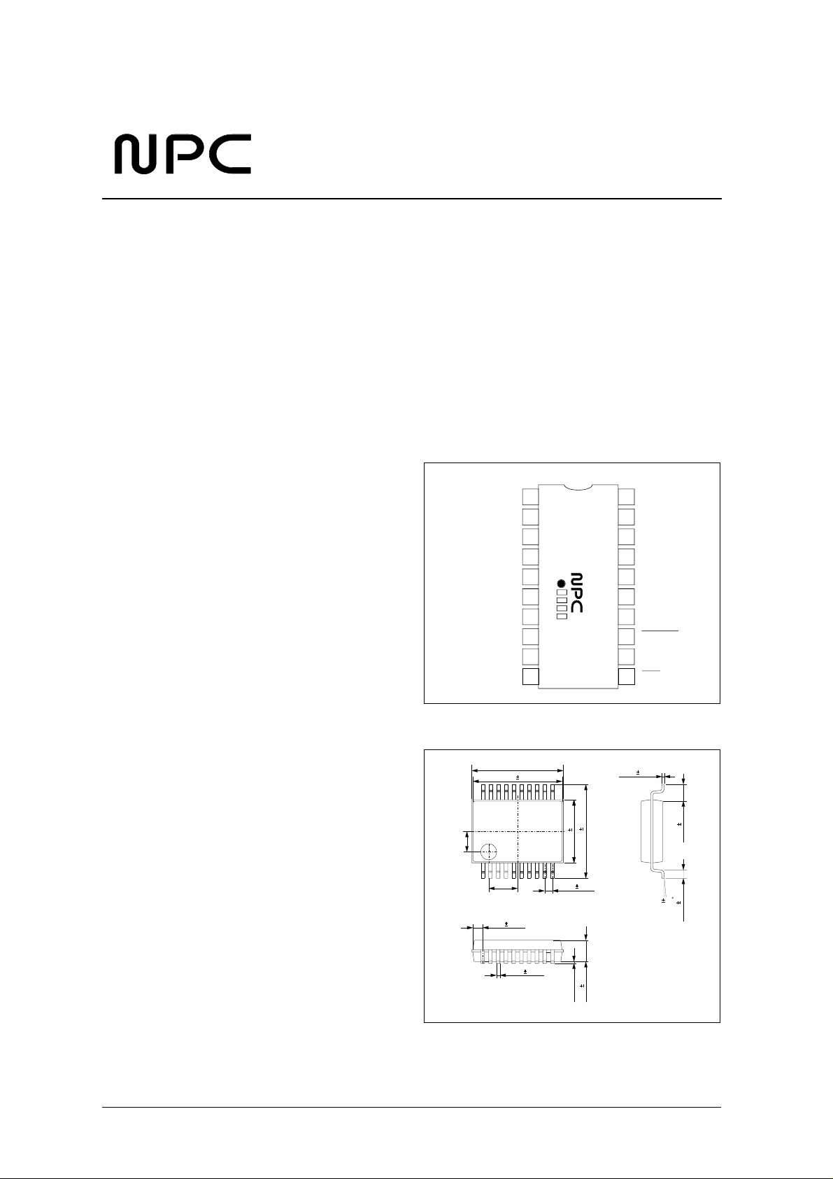
The SM8211M is available in 20-pin SSOPs.
FEATURES
■
Conforms to POCSAG standard for pagers
■
512 or 1200 bps signal speed
■
Supports tone, numeric or character call messages
■
Battery-saving function for low battery consumption
■
BS1 (RF control main output signal) and BS3
(PLL setup signal) 60-step setup time setting—for
BS3, 50.8 ms (max) at 1200 bps and 119.1 ms
(max) at 512 bps
Note that (BS3 setup time) − (BS1 setup time)
should be set to ≥ 2.
■
BS2 (RF DC-level adjustment signal) before/during reception selectable adjustment timing
■
6 addresses × 4 sub-addresses (total of 24
addresses)
■
1-bit and 2-bit burst error auto-correction function
(messages only)
■
25 to 75% duty factor signal coverage (during preamble detection)
■
8 rate error detection condition settings
■
8 receive mode settings
■
76.8 or 153.6 kHz system clock (crystal oscillator
or external clock input)
■
Built-in oscillator capacitor
POCSAG Decoder For Pagers
Built-in input signal filter, with filter ON/OFF and
■
4 selectable filter characteristics
1.2 to 3.5 V (76.8 kHz system clock) or 2.0 to 3.5
■
V (153.6 kHz system clock) operating supply voltage
Molybdenum-gate CMOS process realizes low
■
power dissipation
20-pin SSOP
■
PINOUT
1XVDD
2BS1
3BS2
4BS3
5VDD
6TEST1
7TEST2
8TX-CLK
9TX-DATA
10BREAK 11 RST
PACKAGE DIMENSIONS
7.40max
7.20 0.05
1.50
2.35
0.68 0.12
0.30 0.15
5.30 0.05
0.65 0.12
− 0.10
+ 0.05
0.15
SM8211M
7.90 0.20
1.80 0.05
20 XTN
19 XT
18 SYN-VAL
17 RX-CLK
16 ADD-DET
15 VSS
14 SIG-IN
13 BACKUP
12 RX-DATA
0.20 0.05
4
4
1.30 0.10
0.60 0.15
NIPPON PRECISION CIRCUITS—1
Page 2
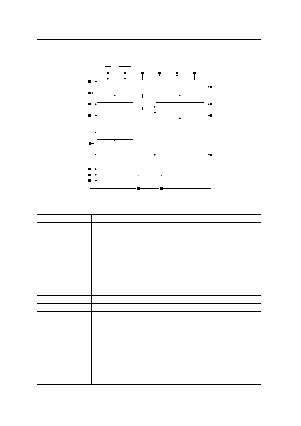
BLOCK DIAGRAM
SM8211M
XT
XTN
TX-CLK
TX-DATA
SIG-IN
VDD
XVDD
VSS
PIN DESCRIPTION
RST
BACKUP
Flag register
Address register
Receive data register
Digital PLL
BREAK BS1 BS2 BS3
Timing control
Data comparator
Preamble pattern
Sync code
Idle code
Error correction
TEST1 TEST2
RX-CLK
ADD-DET
SYN-VAL
RX-DATA
Number Name I/O Description
1 XVDD – Oscillator circuit supply pin. Capacitor connected between XVDD and VSS.
2 BS1 O RF control main output signal
3 BS2 O RF DC-level adustment signal
4 BS3 O PLL setup signal
5 VDD – Supply voltage
6 TEST1 I Test pin. Leave open for normal operation.
7 TEST2 I Test pin. Leave open for normal operation.
8 TX-CLK I ID data read sync clock
9 TX-DATA I ID data input
10 BREAK I Message transmission interrupt
11 RST
I Hardware reset input
12 RX-DATA O Received data output (to CPU)
13 BACKUP I Power save
14 SIG-IN I NRZ signal input pin
15 VSS – Ground
16 ADD-DET O Address detection output. HIGH on detection
17 RX-CLK O Received data output sync clock
18 SYN-VAL O Sync code detection output. HIGH on detection
19 XT I 76.8 or 153.6 kHz oscillator or external clock input pin
20 XTN O Oscillator output pin
I:Input O:Output
NIPPON PRECISION CIRCUITS—2
Page 3
−
−
−
°
°
−
° C
SM8211M
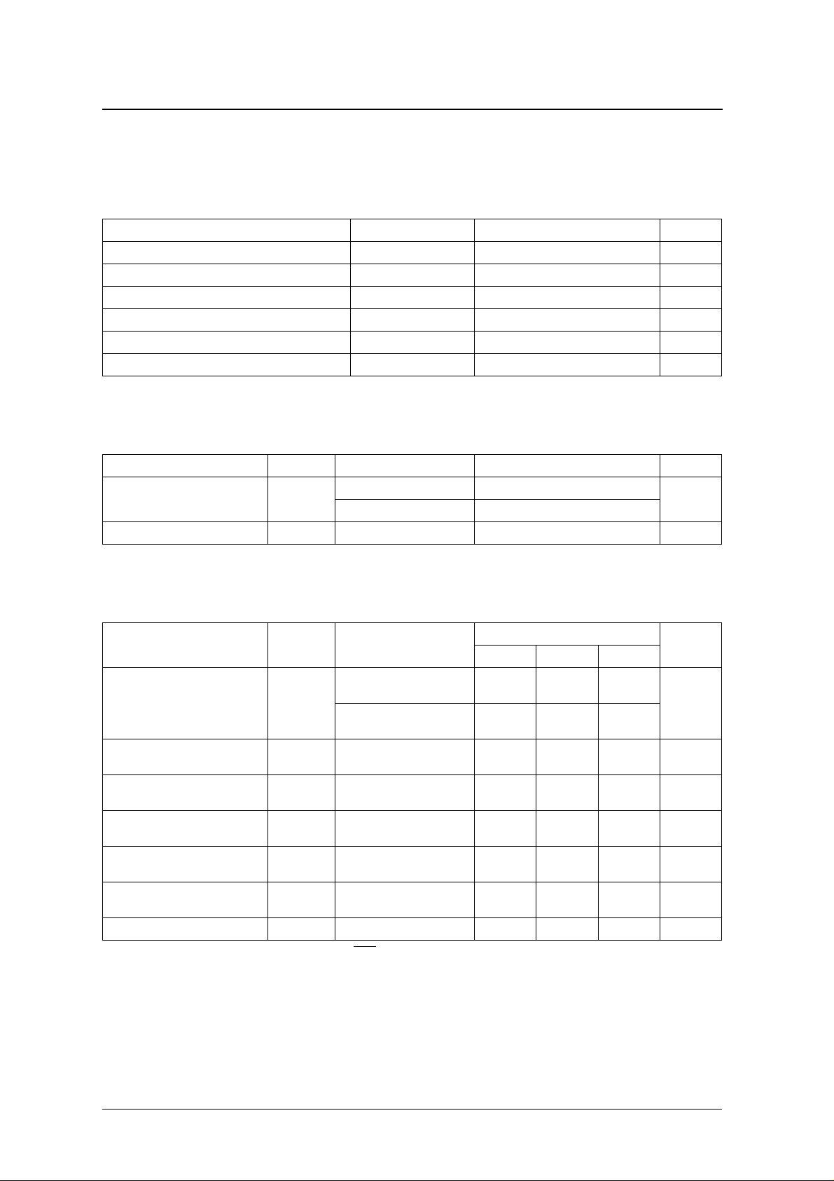
SPECIFICATIONS
Absolute Maximum Ratings
V
= 0 V
SS
Parameter Symbol Rating Unit
Supply voltage range V
Input voltage range V
Power dissipation P
Storage temperature range T
Soldering temperature T
Soldering time t
Recommended Operating Conditions
µ
−
µ
µ
DD
IN
D
stg
sld
sld
0.3 to 7.0 V
0.3 to V
+ 0.3 V
DD
250 mW
40 to 125
260
10 s
C
C
V
= 0 V
SS
Parameter Symbol Condition Rating Unit
76.8 kHz system clock 1.2 to 3.5
Supply voltage range V
Operating temperature range T
DD
opr
153.6 kHz system clock 2.0 to 3.5
DC Characteristics
V
= 1.2 to 3.5 V, V
DD
Parameter Symbol Condition
Consumption current
HIGH-level input voltage
(all inputs)
LOW-level input voltage
(all inputs)
HIGH-level output voltage
(all outputs except XTN)
LOW-level output voltage
(all outputs except XTN)
Input leakage current
(all inputs except XT)
Standby supply current I
1. The consumption current is slightly higher when RST is going LOW.
SS
1
= 0 V, T
= − 20 to 70 ° C unless otherwise noted
a
XT = 76.8 kHz,
V
= 3.5 V
I
V
V
V
V
I
DDS
DD
IH
IL
OH
OL
IL
DD
XT = 153.6 kHz,
V
= 3.5 V
DD
I
= − 20 µ A, V
OH
I
= 20 µ A, V
OH
V
= V
IN
DD
T
= 25 ° C – – 1.0
a
= 2.0 V V
DD
= 2.0 V – – 0.1 V
DD
or V
SS
20 to 70
Rating
min typ max
– 20.0 30.0
– 25.0 35.0
0.8V
DD
– – 0.2V
0.1 – – V
DD
––V
DD
–– ± 1.0
V
Unit
A
V
A
A
NIPPON PRECISION CIRCUITS—3
Page 4
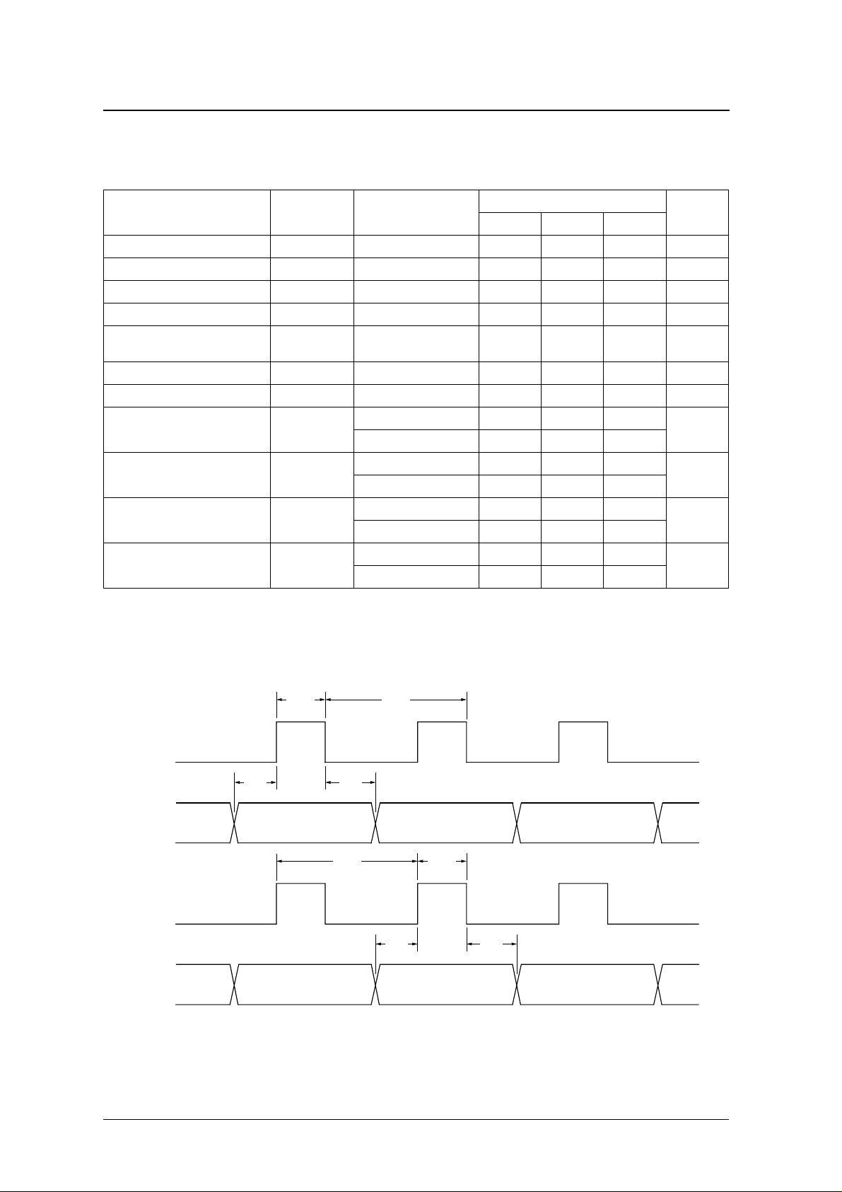
AC Characteristics
V
= 1.2 to 3.5 V, V
DD
SS
= 0 V, T
SM8211M
= − 20 to 70 ° C unless otherwise noted
a
µ
µ
µ
µ
−
µ
µ
µ
µ
µ
Parameter Symbol Condition
TX-CLK pulsewidth t
TX-CLK pulse cycle t
TX-DATA setup time t
TX-DATA hold time t
XT pulse frequency t
XT pulse duty cycle D
BREAK pulsewidth t
RX-CLK pulse cycle
RX-CLK pulsewidth
RX-DATA lead time
RX-DATA hold time
1
1
1
1
PWTX
CYTX
STX
HTX
CYXT
PWBR
t
CYRX
t
PWRX
t
SRX
t
HRX
XT
512 bps – 1953 –
1200 bps – 833 –
512 bps – 124 –
1200 bps – 52 –
512 bps – 1341 –
1200 bps – 573 –
512 bps – 488 –
1200 bps – 208 –
1. Internal digital PLL operation is subject to some change.
Rating
Unit
min typ max
13 – 100
450 – –
1.0 – –
1.0 – –
250 ppm
76.8 or
153.6
+250 ppm kHz
s
s
s
s
25–75%
13 – –
s
s
s
s
s
AC timing
TX-CLK
TX-DATA
RX-CLK
RX-DATA
t
PWTX
t
STX
t
CYRX
t
CYTX
t
HTX
t
PWRX
t
SRX
t
HRX
NIPPON PRECISION CIRCUITS—4
Page 5
SM8211M
FUNCTIONAL DESCRIPTION
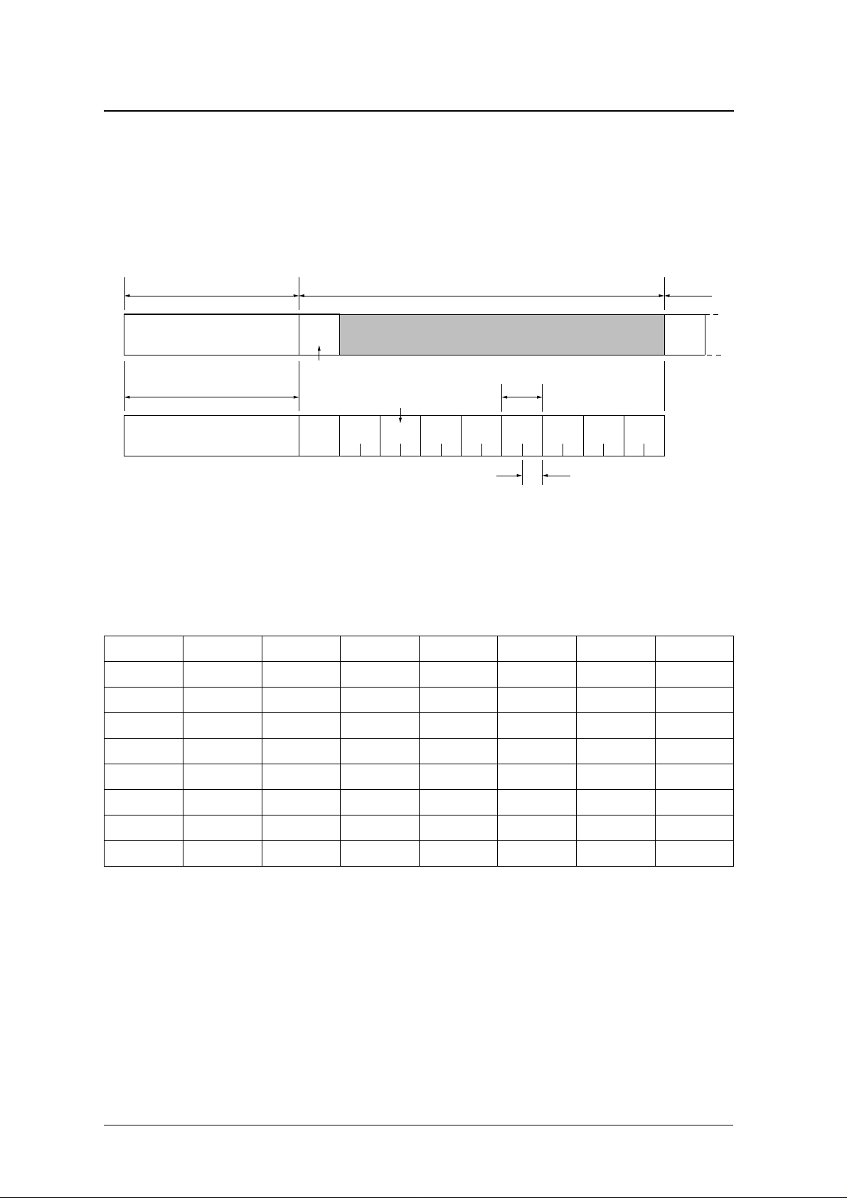
Receive Format
The receive format conforms to CCIR RPC No. 1
(POCSAG).
Preamble
SC SC
1st batch
2nd and
successive
batches
Continuous 576-bit "1,0" bit pattern
... 1 0 1 0 1 0 1 0 1 0 ...
Sync code word
Frame number
0SC 1234567
1 code word (32 bits)
1 frame (= 2 code words)
Figure 1. Receive signal format
Sync signal (SC)
The sync signal is a continuous code word in the
received signal, used for word synchronization. It
even-parity bit, making a 32-bit signal. The sync
code word pattern is shown in table 1.
comprises 31 bits in an M-series bit pattern plus one
Table 1. Sync code word
Bit number Bit value Bit number Bit value Bit number Bit value Bit number Bit value
1091170251
2 1101180261
3 1110190270
4 1121201281
5 1130210291
6 1140221300
7 0151230310
8 0160241320
NIPPON PRECISION CIRCUITS—5
Page 6
SM8211M
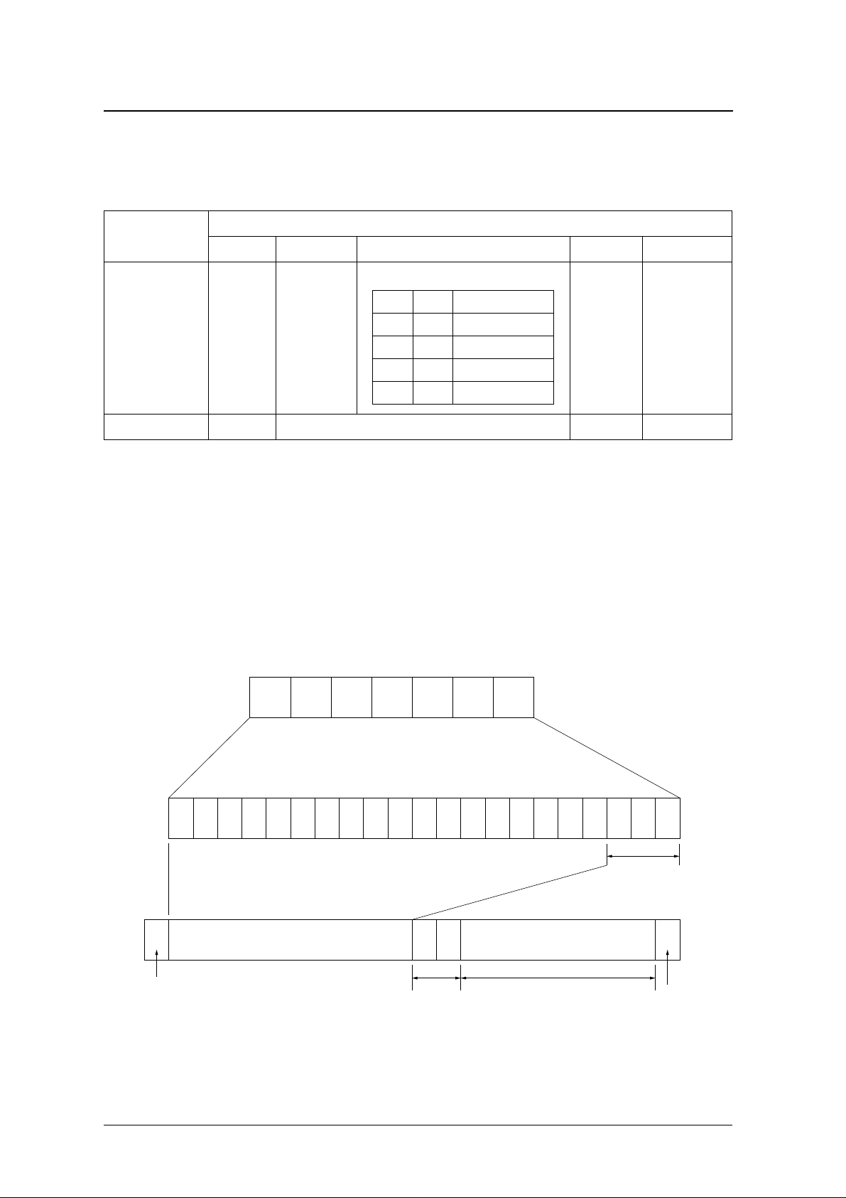
Code words (address and message signals)
Each code word comprises 32 bits as shown in table 2.
Table 2. Code word format
Code word
1 (MSB)
1
2 to 19
2
20, 21
2
22 to 31
3
32 (LSB)
4
Function bits
20 21 Function
0 0 A call
Bit number
Address signal 0 Address bits
0 1 B call
Check bits Even-parity bit
1 0 C call
1 1 D call
Message signal 1 Message bits Check bits Even-parity bit
1. The MSB is the address/message code word control bit. It is 0 for an address signal, and 1 for a message signal.
2. Bits 2 to 21 contain the address or message information.
3. Bits 22 to 31 are BCH(31,21) f ormat generated check bits , where BCH(n,k) = BCH(w ord length, number of information bits).
4. The LSB is an even-parity bit for bits 1 to 31.
Call number to call sign conversion
This conversion expands a 7-digit decimal call number into a 21-bit binary call sign, as shown in figure
2.
bits are the user-defined frame identification pattern,
which is stored in ID-ROM. The two function bits
define which of four call functions is active.
After expansion, the high-order 18 bits are assigned
to bits 2 to 19 (address signal), and the low-order 3
7-digit decimal call
signal (gap code)
MSB LSB
21-bit binary
conversion
Call sign
1 2 3 4 5 6 7 8 9 10 11 12 13 14 15 16 17 18 19 20 21
Flag:
0 = address signal
1 = message signal
1
2 3 4 5 6 7
Bits 2 to 19 (18 bits)
20 21 321 Bits 22 to 31 (10 bits)
Function bits BCH(31,21) generated check bits
Figure 2. Call number to call sign conversion
Frame
identificaton
pattern
Even-parity bit
(for bits 1 to 31)
NIPPON PRECISION CIRCUITS—6
Page 7
SM8211M
Idle signal (dummy signal)
An idle word can be inserted into either the address
or message signal to indicate that the word contains
no information. The idle word bit pattern is shown in
table 3. Message reception is halted when the
receiver detects an idle word.
In pager systems that send numeric data, the number
of frames varies with the type of message being sent.
In this case, an idle signal is transmitted to indicate
completion of the message.
Table 3. Idle code word
Bit
number
1 0 17 1
2 1 18 1
3 1 19 0
4 1 20 0
5 1 21 0
6 0 22 0
7 1 23 0
8 0 24 1
9 1 25 1
100260
110270
120281
131290
140301
150311
Bit value
Bit
number
Bit value
Battery Saving (BS1, BS2, BS3)
The SM8211M controls the intermittent-duty operation of the RF stage, which reduces battery consumption, and outputs three control signals (BS1, BS2,
BS3). The function each signal controls in each
mode is described below.
■ BS1 (RF-control main output signal)—The RF
stage is active when BS1 is HIGH. The risingedge setup time for receive timing is set by flags
RF0 to RF5 (60 steps). The maximum setup time
is 49.167 ms at 1200 bps, and 115.234 ms at 512
bps.
Note that 3C, 3D, 3E and 3F are invalid settings
for BS1.
■ BS2 (RF-control output signal)—BS2 is used to
control the discharge of the receive signal DC-cut
capacitor. The function of BS2 is determined by
flag BS2, as described below.
• When flag BS2 is 0, pin BS2 goes HIGH
together with BS1 and then goes LOW again
after the BS1 setup time. However, in lock
mode (during address/message reception), it
stays LOW.
• When flag BS2 is 1, pin BS2 goes HIGH during
lock mode sync code receive timing, and preamble mode and idle mode signal receive timing.
■ BS3 (RF-control output signal)—BS3 is used to
control PLL operation when the PLL is used. The
rising-edge setup time for receive timing is set by
flags PL0 to PL5 (60 steps). The maximum setup
time is 50.833 ms at 1200 bps, and 119.141 ms at
512 bps.
Note that 3E and 3F are invalid settings for BS3.
Note also that (BS3 rising-edge setup time) − (BS1
rising-edge setup time) should be ≥ 2.
161321
Receive signal duty factor
During preamble detection, the preamble pattern
(1,0) is recognized at duty factors from 25% (min) to
75% (max) of the (1,0) preamble cycle.
NIPPON PRECISION CIRCUITS—7
Page 8

SM8211M
Operating Modes
The SM8211M has four operating modes—SwitchON, Preamble, Idle and Lock modes. Note that all
values in parentheses in the following figures are for
the case when the speed is 1200 bps.
Switch-ON mode
After power is applied and after RST has gone LOW
to reset all internal circuits, code words for the 27-bit
flag data and the six 18-bit addresses are received
from the CPU on TX-DATA and are stored. As each
code word comprises 32 bits, this process takes (32 ×
RST
7) + 1 TX-CLK cycles to complete. When the 225
TX-CLK cycles have been received, BS1, BS2 and
BS3 are set and device operation transfers to preamble mode.
TX-CLK
TX-DATA
BS1
BS2
(BS2 flag = 0)
BS2
(BS2 flag = 1)
1 to 200 ms
X
1 2 224 225
127 ms (54.2 ms)
1.953 x N ms
(0.833 x N ms)
1.953 x M ms
(0.833 x M ms)
BS3
X > 2 ms for external system clock operation or during continuous oscillations
X > 900 ms for internal oscillator operation immediately after power is applied or BACKUP is released (V = 1.5 to 3.5 V)
X > 1.5 s for internal oscillator operation immediately after power is applied or BACKUP is released (V < 1.5 V)
DD
DD
Figure 3. Switch-ON mode timing
NIPPON PRECISION CIRCUITS—8
Preamble mode
Page 9

SM8211M
Preamble mode
Preamble mode is a continuous 544-bit long period.
If neither a preamble pattern, rate error nor sync code
is detected during this period, operation transfers to
idle mode.
If a preamble pattern is detected, the preamble mode
544-bit long period is recommenced.
If a rate error is detected, device operation transfers
to idle mode. (A single error occurs when two active
edges occur in the received signal on SIG-IN within
1-bit unit time. A rate error occurs when the number
of errors in the error counter equals the error threshold set by flags ER0 to ER2. The error counter is
reset when a preamble pattern is detected.)
If the sync code is detected, SYN-VAL goes HIGH
and operation transfers to lock mode. (If an error of 2
bits or less occurs, the detected word is recognized as
the sync code.)
Idle mode
In idle mode, a check is made for the presence of a
preamble signal when the RF intermittent-duty control signals (BS1, BS2, BS3) for battery saving are
active. If a preamble pattern is detected, operation
immediately transfers to preamble mode. If a preamble pattern is not detected, intermittent-duty operation continues.
A preamble pattern is detected when either a 101010
or 010101 6-bit pattern is detected. Since there is a
reasonable probability that this simple pattern can
occur during a valid communicated signal (data, not
preamble), this 6-bit pattern makes returning to preamble mode easier. This is useful for cases where
weak electric fields, noise or other temporary interference cause device operation to transfer to idle
mode. Further, if a sync code is detected within one
cycle after device operation has transferred from
lock mode, device operation returns to lock mode. (If
flag BS2 is 0, pin BS2 does not go HIGH during the
cycle after device operation has transferred from
lock mode.)
BS1
BS2
(BS2 flag = 0)
BS2
(BS2 flag = 1)
BS3
1.953 x N ms
(0.833 x N ms)
62.5 ms
(26.7 ms)
Receive timing
1.953 x M ms
(0.833 x M ms)
Figure 4. Idle mode timing
Preamble signal
Preamble count starts
Figure 5. Preamble pattern sequence
1062.5 ms (453.3 ms)
Error bit
... 1 0 1 0 1 1 1 0 1 0 1 0 1 0 1 0 1 0 1 0 ...
Counting
Count reset to 0
Preamble count restarts
X
Preamble detected
NIPPON PRECISION CIRCUITS—9
Page 10

Lock mode
SM8211M
If the sync code is detected during the preamble
period, device operation transfers to lock mode and
BS1 goes LOW. BS1 then goes HIGH again under
frame timing, where the frame number is set by flags
FF0 to FF2, and the 24 addresses are compared with
ID-ROM (If the frame number is 0, BS1 stays
HIGH). If errors of 2 bits or less occur, the address is
still recognized. Since there are two code words per
frame, this check is done twice.
When one of the 24 addresses does not match, BS1
goes LOW and the device waits for the next sync
code receive timing. If the sync code is still not
detected after two consecutive attempts, device operation transfers to idle mode, except during message
reception where operation stays in lock mode. If the
sync code is not detected on the second attempt, but
instead a pattern forming a preamble is detected,
device operation transfers to preamble mode and not
idle mode (preamble mode is more advantageous for
sync code detection).
When one of the 24 addresses does match, ADDDET goes HIGH for the duration of the next code
word period and the corresponding 5-bit address
information is transmitted to the CPU on RX-DATA
in sync with RX-CLK. When the address information is confirmed, BS1 is held HIGH and the message is received. The 20-bit error-corrected message
data, a 2-bit error correction result code and an evenparity bit form a 23-bit word that is sent to the CPU
on RX-DATA in sync with RX-CLK. When an
incoming message spans two or more batches, additional sync code detection occurs during sync code
receive timing.
Message reception ends when an address code or
idle code is detected, or when interrupted using the
BREAK input. When message reception ends, BS1
goes LOW and the device w aits for either the address
detect timing of the next frame or the sync code
receive timing.
Switch-ON mode
A
Preamble mode
B
C
D
Idle mode Lock mode
E
G
F
Figure 6. Operating mode transition diagram
A: After RST goes LOW, ID code is read in sync with TX-CLK
B: Rate error or, within a fixed period, preamble pattern or sync code not detected
C: Preamble pattern detected
D: Sync code detected 1 cycle immediately after transferring from lock mode
E: Sync code not detected on 2 consecutive attempts
F: Same as E, but preamble pattern detected on the second attempt
G: Sync code detected
NIPPON PRECISION CIRCUITS—10
Page 11

SM8211M
BREAK time
BREAK detection to data halt delay time (2 bits max)
1.953 x M ms at 512 bps
0.833 x M ms at 1200 bps
1.953 x N ms at 512 bps
0.833 x N ms at 1200 bps
Address does not match
1.953 x N ms at 512 bps
0.833 x N ms at 1200 bps
0 1 2 3 4 5 6 7 0 1 2 3 4 5 6 7
ICWSYN ICW ADD MES MES ICW ADD MES MES MES MES ICW ICW ICW ADD MES SYN MES MES MES MES ICW ICW ADD MES MES MES MES ICW ADD MES ADD MES SYN
1.953 x M ms at 512 bps
0.833 x M ms at 1200 bps
0 1 2 3 4 5 6 7 0 1 2 3 4 5 6 7
MESSYN MES ICW ICW ICW ICW ADD MES MES MES MES MES MES MES MES MES SYN MES MES MES ICW ADD MES MES MES MES ICW ADD MES MES ICW ICW ICW SYN
Receive code
BS1
BS2
BS3
(flag BS2 = 1)
Receive code
SYN-VAL
BREAK
ADD-DET
Figure 7. Lock mode timing (frame ID number 3)
BS1
SYN-VAL
BREAK
ADD-DET
NIPPON PRECISION CIRCUITS—11
BS2
(flag BS2 = 1)
BS3
Page 12

SM8211M
Address/Flag Data Transmission (CPU to SM8211M)
After device reset initialization, the address and flag
data is transmitted from the CPU on TX-DATA in
225 cycles in sync with the falling edge of TX-CLK.
(See the description in “Switch-ON mode”).
The SM8211M supports six independent addresses
(identified as A, B, C, D, E and F). Using these, it is
possible to cover all kinds of group calls.
The address data for each of the six addresses comprises an 18-bit address plus two function bits used
to select one of four sub-addresses. Then, one MSB
bit (0 for address signals), ten BCH(31,21) format
to form 32-bit code words representing the address
information which is then stored in RAM. This
address information is then compared with the
received data to determine correct addressing.
If the number of addresses used is less than six, the
same address should be repeated as many times as
necessary to cancel the remaining addresses. Also,
each 18-bit address should be input MSB first.
The TX-CLK cycle and corresponding address data
bits are shown in table 4, and the function of each
flag is shown in tables 5 to 13.
generated check bits and an even-parity bit are added
Table 4. Address/flag transmit format
TX
Data
TX
Data
TX
Data
TX
Data
TX
Data
TX
Data
TX
Data
TX
Data
TX
clock
bit
clock
bit
clock
bit
clock
1 0 27 FL1 53 0 79 AB3 105 AC9 131 AD15 157 0 183 0 209 AF1
2 SS 28 FL0 54 0 80 AB2 106 AC8 132 AD14 158 0 184 0 210 AF0
3 S1 29 ER2 55 0 81 AB1 107 AC7 133 AD13 159 0 185 0 211 0
4 S0 30 ER1 56 0 82 AB0 108 AC6 134 AD12 160 0 186 0 212 0
5 LBO 31 ER0 57 0 83 0 109 AC5 135 AD11 161 AE17 187 0 213 0
bit
clock
bit
clock
bit
clock
bit
clock
bit
clock
Data
bit
6 FF2 32 0 58 0 84 0 110 AC4 136 AD10 162 AE16 188 0 214 0
7 FF1 33 AA17 59 0 85 0 111 AC3 137 AD9 163 AE15 189 0 215 0
8 FF0 34 AA16 60 0 86 0 112 AC2 138 AD8 164 AE14 190 0 216 0
9 INV 35 AA15 61 0 87 0 113 AC1 139 AD7 165 AE13 191 0 217 0
10 BS2 36 AA14 62 0 88 0 114 AC0 140 AD6 166 AE12 192 0 218 0
11 0 37 AA13 63 0 89 0 115 0 141 AD5 167 AE11 193 AF17 219 0
12 0 38 AA12 64 0 90 0 116 0 142 AD4 168 AE10 194 AF16 220 0
13 0 39 AA11 65 AB17 91 0 117 0 143 AD3 169 AE9 195 AF15 221 0
14 PL5 40 AA10 66 AB16 92 0 118 0 144 AD2 170 AE8 196 AF14 222 0
15 PL4 41 AA9 67 AB15 93 0 119 0 145 AD1 171 AE7 197 AF13 223 0
16 PL3 42 AA8 68 AB14 94 0 120 0 146 AD0 172 AE6 198 AF12 224 0
17 PL2 43 AA7 69 AB13 95 0 121 0 147 0 173 AE5 199 AF11 225 0
18 PL1 44 AA6 70 AB12 96 0 122 0 148 0 174 AE4 200 AF10
19 PL0 45 AA5 71 AB11 97 AC17 123 0 149 0 175 AE3 201 AF9
20 RF5 46 AA4 72 AB10 98 AC16 124 0 150 0 176 AE2 202 AF8
21 RF4 47 AA3 73 AB9 99 AC15 125 0 151 0 177 AE1 203 AF7
22 RF3 48 AA2 74 AB8 100 AC14 126 0 152 0 178 AE0 204 AF6
23 RF2 49 AA1 75 AB7 101 AC13 127 0 153 0 179 0 205 AF5
24 RF1 50 AA0 76 AB6 102 AC12 128 0 154 0 180 0 206 AF4
25 RF0 51 0 77 AB5 103 AC11 129 AD17 155 0 181 0 207 AF3
26 FL2 52 0 78 AB4 104 AC10 130 AD16 156 0 182 0 208 AF2
NIPPON PRECISION CIRCUITS—12
Page 13

Table 5. Flag functions
Flag Function
SS Receive mode set ON/OFF. ON when 1.
S0, S1 One of eight operating conditions select (with LBO when SS is 1)
LBO 512/1200 bps speed select. 512 bps when 1.
FF0 to FF2 Frame number select
INV Signal input (SIG-IN) normal/inverse select. Normal when 0.
BS2 BS2 output signal mode select
PL0 to PL5 BS3 output signal rising-edge setup time for receive timing
RF0 to RF5 BS1 output signal rising-edge setup time for receive timing
FL2 Internal digital filter ON/OFF. ON when 1.
FL0, FL1 Digital filter parameter select (when FL2 is 1)
ER0 to ER2 Rate error detection threshold select
SM8211M
Table 6. Receive mode set flags
SS S1 S0 LBO
PL5 PL4 PL3 PL2 PL1 PL0 RF5 RF4 RF3 RF2 RF1 RF0 FL2 FL1 FL0 ER2 ER1 ER0
1000111101001010101001
1010111101001100101001
1100111101001110101001
1110111101010001000001
1001011011000100101001
1011011011000101101001
1101011011000110101001
1111011011000111000001
0 ××0
0 ××1
1. × = don’t care
Table 7. Baud rate flag
LBO Baud rate
1
Set flags
All other combinations not set automatically
Table 9. BS2 flag
BS2 BS2 operating mode
0 1200 bps
1 512 bps
Table 8. Input polarity flag
INV Polarity
0 Normal
1 Inverse
0 See the description in
1
NIPPON PRECISION CIRCUITS—13
section “Battery Saving
(BS1, BS2, BS3)”
Page 14

SM8211M
Table 10. Frame number flags
FF2 FF1 FF0 Frame number
000 0
001 1
010 2
011 3
100 4
101 5
110 6
111 7
Table 11. PLL setup time flags/BS1 rising-edge
setup time flags
PL5
PL4
(RF5)
(RF4)
0000000.000 ms 0.000 ms
0000010.833 ms 1.953 ms
PL3
(RF3)
1
PL2
(RF2)
PL1
(RF1)
PLL setup time
(BS1 rising-edge setup
PL0
(RF0)
LBO = 0 LBO = 1
time)
Table 13. Rate error detection set flags
ER2 ER1 ER0 Rate error threshold
0 0 0 Count = 1
0 0 1 Count = 2
0 1 0 Count = 3
0 1 1 Count = 4
1 0 0 Count = 5
1 0 1 Count = 6
1 1 0 Count = 7
1 1 1 Count = 8
0000101.667 ms 3.906 ms
↓↓↓↓↓↓ ↓ ↓
01111125.833 ms 60.547 ms
10000026.667 ms 62.500 ms
10000127.500 ms 64.453 ms
↓↓↓↓↓↓ ↓ ↓
11110150.833 ms 119.141 ms
1. Note that (BS3 rising-edge setup time) − (BS1 rising-edge setup
time) should be ≥ 2.
Table 12. Digital filter constant set flags
1
FL2 FL1 FL0 Filter constant
0 ××Digital filter not used
1 0 0 Filter constant 1
1 0 1 Filter constant 2
1 1 0 Filter constant 3
1 1 1 Filter constant 4
1. × = don’t care
NIPPON PRECISION CIRCUITS—14
Page 15

SM8211M
Received Data Transmission (SM8211M to CPU)
In lock mode, if the receive data for the frame is recognized as one of the 24 addresses with 2 bit errors
or less, then ADD-DET goes HIGH for the duration
Detected address codeword
Internal bit
clock
27 28 29 30 31 0 1 2 3 4 5 6 7 8 9 10 11 12 13 14 15 16 17 18 19 20 21 22 23 24 25 26 27 28 29 30 31 0 1
RX-CLK
RX-DATA
ADD-DET
Figure 8. Received address transmit timing
Table 14. Address set flags
of the next code word period and the corresponding
5-bit address information is transmitted to the CPU
on RX-DATA in sync with RX-CLK.
1 codeword
A0 A1 A2 A3 A4
A0 A1 A2 A3 A4 Address Function A0 A1 A2 A3 A4 Address Function
00100
10100 B call 10001 B call
A
01100 C call 01001 C call
11100 D call 11001 D call
00010
10010 B call 10101 B call
B
01010 C call 01101 C call
11010 D call 11101 D call
00110
10110 B call 10011 B call
C
01110 C call 01011 C call
11110 D call 11011 D call
A call 00001
A call 00101
A call 00011
A call
D
A call
E
A call
F
NIPPON PRECISION CIRCUITS—15
Page 16

SM8211M
When an address is detected, the next 32-bit data
code word is received. The BCH(31,21) format error
check bits are checked and if a 1-bit or two consecutive bit errors occur, they are corrected. Two random
bit errors, or three or more bit errors are not corrected. If the corrected data MSB is 1, the data is rec-
Received message codeword
Internal bit
clock
27 28 29 30 31 0 1 2 3 4 5 6 7 8 9 10 11 12 13 14 15 16 17 18 19 20 21 22 23 24 25 26 27 28 29 30 31 0 1
RX-CLK
20-bit error-corrected message data
RX-DATA
Figure 9. Received message transmit timing
Table 15. Error count flags
E0 E1 Error count
ognized as a message, data reception continues and
the corrected message data and error check flags are
sent to the CPU. If the MSB is 0, the data is recognized as an address signal or idle code and data
reception or data transmission to the CPU is halted.
1 codeword
PEE1E0
Table 16. Parity check flag
PE Even-parity check result
1
0 0 No errors
1 0 1-bit error
0 1 Two consecutive bit errors
11
Two random, or three or more
bit errors
CPU Interface
SYN-VAL
If a sync code is detected with two bit errors or less
during sync code detection timing while in preamble,
lock or idle mode, SYN-VAL goes HIGH for the
duration of the next batch (544 bits long).
ADD-DET
If frame data is received and recognized with two bit
errors or less while in lock mode, ADD-DET goes
HIGH for the duration of the next code word period.
If an address is detected in the second code word in
the frame, ADD-DET stays HIGH for the duration of
two code word periods.
0 No errors
1 An error occurred
1. The even-parity check is performed on the data before error correction.
BREAK
On a rising edge of BREAK, message reception and
received message transmission are halted. After a
BREAK interrupt, the device waits for frame address
detection or sync code detection timing. This function is useful in cases of continuing message reception, because without sync code or other detection
taking place the received data would be deemed to
have many errors.
NIPPON PRECISION CIRCUITS—16
Page 17

Extended Reset
SM8211M
When RST goes LOW for 1 to 2 ms or longer, BS1
and BS3 together go HIGH. Approximately 1 to 2 ms
after RST goes HIGH, device operation continues.
When RST is LOW for less than 200 ms
RST
1 to 2 ms
BS1
BS3
Figure 10. Extended reset timing
When RST
If the RST LOW-level pulsewidth exceeds 200 ms,
the parameters for switch-ON mode should be
quickly set over again as soon as RST returns HIGH.
is LOW for more than 200 ms
This function is useful for checking the RF stage circuits. After RST goes HIGH, the device waits for the
ID code input.
1 to 2 ms
RST
TX-CLK
TX-DATA
BS1
BS3
> 200 ms
1 to 200 ms
DATA
BS3 can also follow the dashed line during this interval.
Figure 11. Extended reset timing (≥ 200 ms)
For internal oscillator operation, RST goes LOW for
1 ms or longer immediately after power is applied or
just after a BACKUP release. After RST returns
HIGH, a wait time of approximately 900 ms (VDD =
1.5 to 3.5 V) or 1.5 s (VDD < 1.5 V) should be
observed before operation starts.
NIPPON PRECISION CIRCUITS—17
Page 18

Power Save Control
SM8211M
When BACKUP goes LOW, the internal operation
stops and all outputs go high impedance. When
power save mode is released for normal operation,
switch-ON mode internal initialization and ID code
re-setting is required. The XT clock and TX-CLK
timing when BACKUP goes LOW is described
below.
RST
XT
TX-CLK
TX-DATA loading
During TX-DATA loading, TX-CLK should be
maintained and not stopped until the ID code is read
in.
Also, the XT clock should be maintained until after
the equivalent time of 1 bit after the ID code is read
in (150 cycles at 512 bps and 64 cycles at 1200 bps).
BACKUP
BACKUP
ENABLE
(internal)
Figure 12. TX-DATA load timing
TX-DATA when not loading
After BACKUP has gone LOW, the XT clock should
be maintained for the equivalent time of 65 bits or
longer.
Input Signal Digital Processing (Digital
Filter)
In pagers, two baud rates, 512 and 1200 bps, are in
use. The current method of ensuring the most suitable reception conditions is to substitute RF-stage
LPF constants that are proportional to the baud rate.
In the SM8211M, digital processing of the signal
input deals with both baud rates without substituting
RF-stage LPF constants. W ith this digital processing,
a particularly small rise in the rate error probability
can be expected.
1 bit equivalent time
System Clock
The SM8211M operates using a 76.8 or 153.6 kHz
system clock. The clock can be set up using a crystal
oscillator or an externally input clock.
For crystal oscillator clocks, only a crystal needs to
be connected between XT and XTN. The oscillator
amplifier, feedback resistor and oscillator capacitor
are all built-in.
For externally input clocks, the clock is connected to
XT through a 100 pF to 0.1 µF coupling capacitor.
In both cases, crystal oscillator and external clock, a
supply decoupling capacitor of 1000 pF to 0.1 µF
should be connected between XVDD and VSS. Also,
the output on XTN should not be used as a clock to
drive an external device.
The digital processing can be set ON or OFF using
flag FL2, and when ON, there are four filter constant
settings that can be set using flags FL0 and FL1 to
obtain the most suitable reception conditions in a
flexible manner. (See table 12.)
NIPPON PRECISION CIRCUITS—18
Page 19

FLOWCHARTS
Switch ON Preamble Idle
SM8211M
No
No
No
RST = LOW
BS1 = BS3 = LOW
RST = HIGH
BS1 = BS3 = LOW
TX-CLK count reset (T = 0)
TX-CLK increment (T = T + 1)
ID code and flags read in
T = 225
Yes
Yes
Yes
Bit clock counter reset (T = 0) BS3 output timing
Bit clock count increment
(T = T + 1)
BS1 = BS2 = HIGH
Preamble pattern
No
Sync code detected
No
Rate error
No
No
T = 544
Yes
Yes
Yes
Yes
Just transferred from
Preamble present
No
Receive timing finished
Yes
BS3 = HIGH
(BS1 = HIGH)
BS2 = LOW
(BS2 = HIGH)
lock mode
No
No
No
Yes
BS1 = BS3 = LOW
ID code and flags set
BS3 = HIGH
BS1 = BS2 = HIGH
(BS1 = HIGH)
BS2 = LOW
(BS2 = HIGH)
Preamble Idle Lock Preamble
Parentheses indicate operation with flag BS2 = 1.
(BS1 = BS2 = BS3 = LOW)
No
SYN-VAL = HIGH
BS1 = BS3 = LOW
(BS1 = BS2 = BS3 = LOW)
Sync code detected
Yes
Yes
NIPPON PRECISION CIRCUITS—19
Page 20

Lock
SM8211M
A
(BS1 = BS2 = BS3 = LOW)
BS1 = HIGH, BS3 = HIGH
setup times for frames
B
Message receive flag = 1
Frame = 0
No
BS1 = BS3 = LOW
Address detected
Yes
No
Yes
BS2 = LOW BS1 = BS3 = LOW
Message receive flag = 0
Sync code timing
Frame timing < frame
Frame timing = frame
Frame = 7
No
Yes
ADD-DET = HIGH
address information transmit
Sync code timing
No
C
Frame timing
No
Message/Address
Message Message
Message transmit
Yes
Yes
Address
No
Message/Address
Address
Valid address
Yes
BS1 = BS3 = LOW
BS1 = HIGH, BS3 = HIGH
setup times for
sync code timing
(BS2 = HIGH)
E
NIPPON PRECISION CIRCUITS—20
Page 21

SM8211M
BREAK input
Message receive flag = 0
and message halts
within 2 bits of time
E
Sync code detected
Yes
SYN-VAL = HIGH
Frame timing
= frame
No
Wait until next code word
D
No
SYN-VAL = HIGH
Yes
SYN-VAL = LOW Preamble present
No
Yes
B
Yes
Message receive flag
0
A
No
1
Message receive flag
1
(BS1 = BS2 = BS3 =LOW)
C
0
BS1 = BS3 = LOW
Idle Preamble
NIPPON PRECISION CIRCUITS—21
Page 22

SM8211M
TYPICAL APPLICATIONS
RF stage Decoder Alert
RF
Paging Receiver System
Waveform
generator
D/D converter
Supply Display
SM8211M
decoder IC
CPU
LCD driver
LCD
Amplifier
ID-ROM
SP
NIPPON PRECISION CIRCUITS INC. reserves the right to make changes to the products described in this data
sheet in order to improve the design or performance and to supply the best possible products. Nippon Precision
Circuits Inc. assumes no responsibility for the use of any circuits shown in this data sheet, conveys no license
under any patent or other rights, and makes no claim that the circuits are free from patent infringement.
Applications for any devices shown in this data sheet are for illustration only and Nippon Precision Circuits Inc.
makes no claim or warranty that such applications will be suitable for the use specified without further testing or
modification. The products described in this data sheet are not intended to use for the apparatus which influence
human lives due to the failure or malfunction of the products. Customers are requested to comply with applicable
laws and regulations in effect now and hereinafter, including compliance with export controls on the distribution
or dissemination of the products. Customers shall not export, directly or indirectly, any products without first
obtaining required licenses and approvals from appropriate government agencies.
NIPPON PRECISION CIRCUITS INC.
4-3, Fukuzumi 2-chome
Koto-ku, Tokyo 135-8430, Japan
NIPPON PRECISION CIRCUITS INC.
Telephone: 03-3642-6661
Facsimile: 03-3642-6698
NC9402DE 1995.04
NIPPON PRECISION CIRCUITS—22
 Loading...