

Page 1
SM8145A
NIPPON PRECISION CIRCUITS INC.
Dual EL Driver
OVERVIEW
The SM8145A is an Electro Luminescent (EL) driver IC that can drive two EL displays simultaneously.
Each EL display mode ON/OFF function can be separately controlled using two enable (ENA) pins.
The luminance in each display mode can be adjusted, enabling the luminance and consumption current to be
optimized to match the application. The device is supplied in ultra-small leadless QFN-20 packages, making
driver circuit miniaturization possible.
FEATURES
■
2 separate EL display drivers
■
2-display simultaneous driver operation
■
Adjustable luminance and current consumption in
each mode
■
3 display modes and a standby mode select control
pins (ENA1, ENA2)
1 to 30cm
■
1.6 to 5.5V supply voltage
■
200 Vp-p maximum EL driver voltage
■
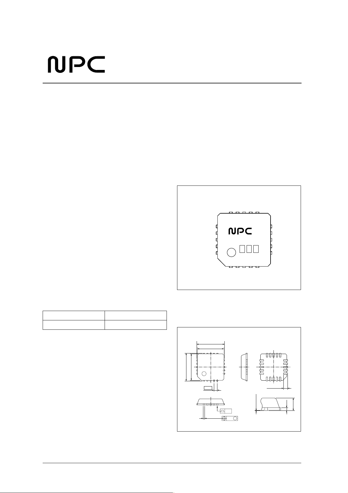
20-pin QFN ultra-small leadless package
■
High voltage CMOS Process
■
2
EL display size per channel
APPLICATIONS
■
Mobile phone
■
PDA, Handheld PC
■
Illumination accessory
PINOUT
(Top view)
OUTCOM
N.C.
OUT1
N.C.
CHV
OUT2
15 14 13 12 11
16
17
18
8145A
19
20
12345
LDR
N.C.
N.C.
VDD
N.C.
VSS
N.C.
ENA1
10
9
8
7
6
OCL1
ENA2
OCE
OCL3
N.C.
OCL2
ORDERING INFORMATION
De vice Pack ag e
SM8145AB 20-pin QFN
PACKAGE DIMENSIONS
(Unit : mm)
Weight : 0.037g
4.20 ± 0.20
4.00 ± 0.10
1115
16
4.00 ± 0.10
4.20 ± 0.20
20
15
0.50
0.22 ± 0.05
10
6
+ 0.03
0.05
M
0.05
NIPPON PRECISION CIRCUITS—1
0.02 − 0.02
0.60 ± 0.10
0.22
1.00max
Page 2
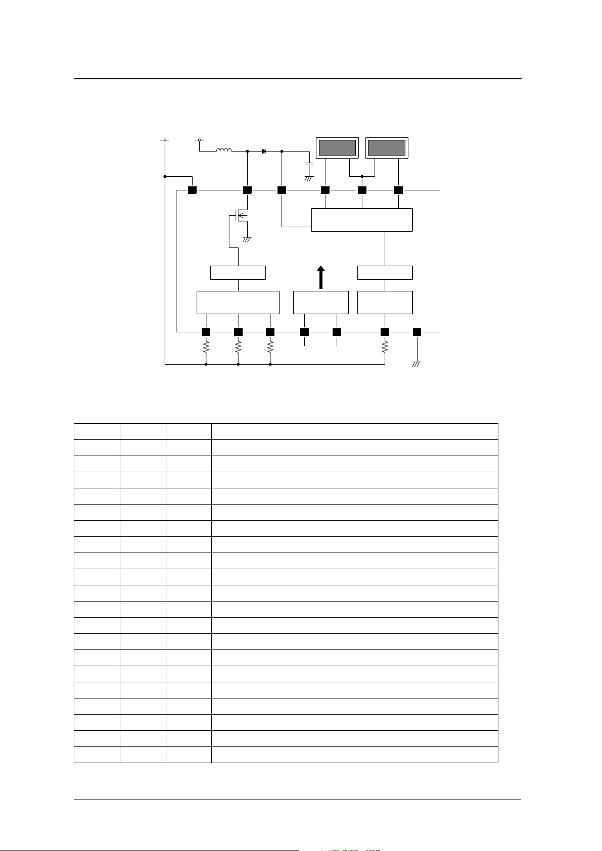
BLOCK DIAGRAM
SM8145A
V
IC VBOOST
PIN DESCRIPTION
VDD CHVLDR
Divider
Oscillator
OCL2OCL1 OCL3
ROCL2ROCL1 ROCL3
EL 1
OUT1
High Voltage Switching Circuit
Control logic
ENA1
ENA2
EL 2
OUTCOM
Divider
Oscillator
OCE
OUT2
R
OCE
VSS
Pin number Name I / O Function
1 L D R O Booster coil driver output
2 N. C. – No connection (must be open)
3 VSS – Ground
4 N. C. – No connection (must be open)
5 OCL1 I Coil driver oscillator 1 (oscillator frequency determined by external resistor)
6 OCL2 I Coil driver oscillator 2 (oscillator frequency determined by external resistor)
7 N. C. – No connection (must be open)
8 OCL3 I Coil driver oscillator 3 (oscillator frequency determined by external resistor)
9 O CE I EL d river oscillator (oscillator frequency determined by exter nal resistor)
10 ENA2 Ip
11 ENA1 Ip
1
Enable input 2 (HIGH: enable, LOW : disable)
1
Enable input 1 (HIGH: enable, LOW : disable)
12 N.C. – No connection (must be open)
13 V D D – Supply
14 N.C. – No connection (must be open)
15 OU T 2 O Output 2
16 O U T C O M O Output (common)
17 N.C. – No connection (must be open)
18 OU T 1 O Output 1
19 N.C. – No connection (must be open)
20 CHV I High-voltage DC input
1. Built-in pull-down resistor.
NIPPON PRECISION CIRCUITS—2
Page 3
C
SM8145A
SPECIFICATIONS
Absolute Maximum Ratings
Parameter Sym bol Condition Rating Unit
Supply voltage range V
Input voltage range V
V
Output voltage
V
V
OUT1/2/COM
Po w er dissipation P
Storage temperature range T
DD
IN
CHV
LDR
D
STG
All Input pins V
CHV pin 0.5 to 120 V
LDR pin 0.5 to 120 V
OUT1, OUT2, OUTCOM pin 0.5 to 120 V
T
≤
70
°
C 140 m W
a
T
≤
85
°
C 100 m W
a
−
0.3 to 7.0 V
−
SS
0.3 to V
−
+ 0.3 V
DD
55 to 125
°
Recommended Operating Conditions
Parameter Sym bol Condition
Supply voltage range V
Ope rating temperature T
Op e rating current
1
Coil inductance L
1. Max value is as same as Absolute Maximum Ratings.
DD2
OPR
I
DD2
LDR
Including coil current, V
Including coil current, V
Including coil current, V
Including coil current, V
f
= 64 kHz – 0.47 – m H
LDR
DD
DD
DD
DD
=
3.0V, T
=
5.0V, T
=
3.0V, T
=
5.0V, T
Rating
min typ max
1.6 3.0 5.5 V
−
40 – 85
≤
70
°
C– – 85 mA
a
≤
70
°
C– – 51 mA
a
≤
85
°
C– – 60 mA
a
≤
85
°
C– – 36 mA
a
Unit
°
C
NIPPON PRECISION CIRCUITS—3
Page 4

DC Characteristics
V
= 3.0 V, T
DD
= 25 ° C unless otherwise noted.
a
SM8145A
Parameter Sym bol Condition
Supply voltage V
CHV output voltage V
OUT1, OUT2, OUTCOM HIGH-level
output voltage
OUT1, OUT2, OUTCOM LOW-level
output voltage
LDR output resistance R
OCE oscillator frequency f
OCE oscillator frequency range f
OCL1, OCL2, OCL3 oscillator frequency f
OCL1, OCL2, OCL3 oscillator frequency
range
OUT1, OUT2, OUTCOM output
frequency
OUT1, OUT2, OUTCOM output
frequency range
LDR inductance driver frequency f
LDR inductance driver frequency range f
ENA1, ENA2 HIGH-level input voltage V
ENA1, ENA2 LOW-level input voltage V
ENA1, ENA2 input current I
ENA1, ENA2 rise time
1
Op e rating current I
Stand-by current I
1.
VDD
SS + 0.5
V
VDD − 0.5
ENA
VSS
CHV
V
OUTH
V
OUTL
LDR
OCE1
OCE2
OCL1
f
OCL2
f
OUT1
f
OUT2
LDR1
LDR2
ENAH
ENAL
ENAH
t
ENA
DD1
STB
Rating
min typ ma x
DD
1.6 3.0 5.5 V
0.5 – 100 V
– – 100 V
– – 0.5 V
I
= 50 mA – 8.0 12.0
LDR
R
= 180 k
OCE
Ω
205 256 307
32 – 1536
R
= 180 k
OCL
Ω
205 256 307
32 – 1536
R
= 180 k
OCE
Ω
200 250 300
31 – 1500
R
= 180 k
OCL
Ω
51 64 77
8 – 384
ENA = HIGH, V
ENA = LOW, V
V
= V
ENAH
= 1.6 to 5.5V V
DD
= 1.6 to 5.5V V
DD
= 3.0V 2.0 4.0 6.0
DD
– 0.5 – V
DD
– 0.3 – V
SS
– – 100 ms
Excluding coil current – – 1.0 mA
ENA = LOW – – 1.0
DD
SS
+ 0.3
+ 0.5
Unit
Ω
kHz
kHz
Hz
kHz
V
µ
A
µ
A
tENA
NIPPON PRECISION CIRCUITS—4
Page 5

FUNCTIONAL DESCRIPTION
;
;
;
;
;
;
;
;;;;;;;;;;;;;;;;;;
DISPLAY MODES
SM8145A
Operation mode
ENA input OUTPUT status Brightness adjust
ENA1 ENA2 O UTCOM OUT1 OUT2 ROCL
Standby LLLLL–
EL 1 H L Active Active Hi-Z R
EL 2 L H Active Hi-Z Active R
EL1 + EL2 H H Active Active Active R
OCL1
OCL2
OCL3
Notes) The internal oscillator resistance is selected in response to the state of the ENA pins.
The oscillator resistance (R
OUT1
OUTCOM
OUT2
EL 1
EL 2
) adjust the luminance in each display mode, respectively.
OCE1/2/3
;;;;;;;;;;;;;;;;;
;;;;;;;;;;;;;;;;;
;;;;;;;;;;;;;;;;;
HI-Z
OFF(0V)
;;;;;;;;;;;;;;;;
HI-Z
;;;;;;;;;;;;;;;;
OFF(0V)
max 100V
0V
max 100V
0V
max 100V
0V
max 200V
max 200VP-P
0-P
0-P
0-P
P-P
ENA1 = LOW
ENA2 = LOW
ENA1 = HIGH
ENA2 = LOW
ENA1 = HIGH
ENA2 = HIGH
ENA1 = LOW
ENA2 = HIGH
NIPPON PRECISION CIRCUITS—5
Page 6

TYPICAL APPLICATIONS
■
EL size: 20 + 20cm
2
, Current consumption: 20 + 20mA
0.1µF
100V
0.01µF
470µH
3.0V
180kΩ
180kΩ
360kΩ
SM8145A
CHV
LDR
OUTCOM
VSS
OCL1
OCL2
OCL3
OUT1
OUT2
VDD
ENA1
ENA2
OCE
180kΩ
EL 20cm
EL 20cm
2
2
■
EL size: 20 + 30cm
■
EL size: 10 + 30cm
Diode: TOSHIBA 1SS250
Coil: MURATA LQH4N471K04M00
2
, Current consumption: 20 + 30mA
0.1µF
100V
CHV
LDR
VSS
OCL1
OCL2
OCL3
0.01µF
470µH
3.0V
180kΩ
270kΩ
430kΩ
Diode: TOSHIBA 1SS250
Coil: MURATA LQH4N471K04M00
2
, Current consumption: 10 + 30mA
OUT1
OUTCOM
OUT2
VDD
ENA1
ENA2
OCE
180kΩ
1kΩ
EL 20cm
EL 30cm
2
2
0.1µF
100V
0.01µF
470µH
3.0V
91kΩ
270kΩ
360kΩ
CHV
LDR
VSS
OCL1
OCL2
OCL3
OUT1
OUTCOM
OUT2
VDD
ENA1
ENA2
OCE
180kΩ
1kΩ
EL 10cm
EL 30cm
2
2
Diode: TOSHIBA 1SS250
Coil: MURATA LQH4N471K04M00
Note: Connect a 1k
Ω
resistor to protect IC when the EL is over 20cm
2
per channel.
Note: Do not operate the SM8145A with the EL NOT connected (no load to OUTCOM/OUT1/OUT2) since the IC will be damaged.
NIPPON PRECISION CIRCUITS—6
Page 7

SM8145A
NIPPON PRECISION CIRCUITS INC. reserves the right to make changes to the products described in this data sheet in order to
improve the design or performance and to supply the best possible products. Nippon Precision Circuits Inc. assumes no responsibility for
the use of any circuits shown in this data sheet, conveys no license under any patent or other rights, and makes no claim that the circuits
are free from patent infringement. Applications for any devices shown in this data sheet are for illustration only and Nippon Precision
Circuits Inc. makes no claim or warranty that such applications will be suitable for the use specified without further testing or modification.
The products described in this data sheet are not intended to use for the apparatus which influence human lives due to the failure or
malfunction of the products. Customers are requested to comply with applicable laws and regulations in effect now and hereinafter,
including compliance with export controls on the distribution or dissemination of the products. Customers shall not expor t, directly or
indirectly, any products without first obtaining required licenses and approvals from appropriate government agencies.
NIPPON PRECISION CIRCUITS INC.
4-3, Fukuzumi 2-chome
Koto-ku, To kyo 135-8430, Japan
Telephone: +81-3-3642-6661
NIPPON PRECISION CIRCUITS INC.
Facsimile: +81-3-3642-6698
http://www.npc.co.jp/
Email: sales
npc.co.jp
@
NC0001AE 2000.10
NIPPON PRECISION CIRCUITS—7
 Loading...