

Page 1
SM8143A
NIPPON PRECISION CIRCUITS INC.
EL Sheet Driver
OVERVIEW
The SM8143A is a transformer-less electroluminescent (EL) driver IC, capable of driving displays up to 80
2
cm
in size. It is a high-efficiency driv er that features re vised coil switching transistor ON resistance and output
circuit configuration to reduce loss.
The EL drive frequency and coil drive frequency can be controlled independently, making the driver circuit
optimizable to match application requirements. A microcontroller interface pin (ENA) is provided, which can
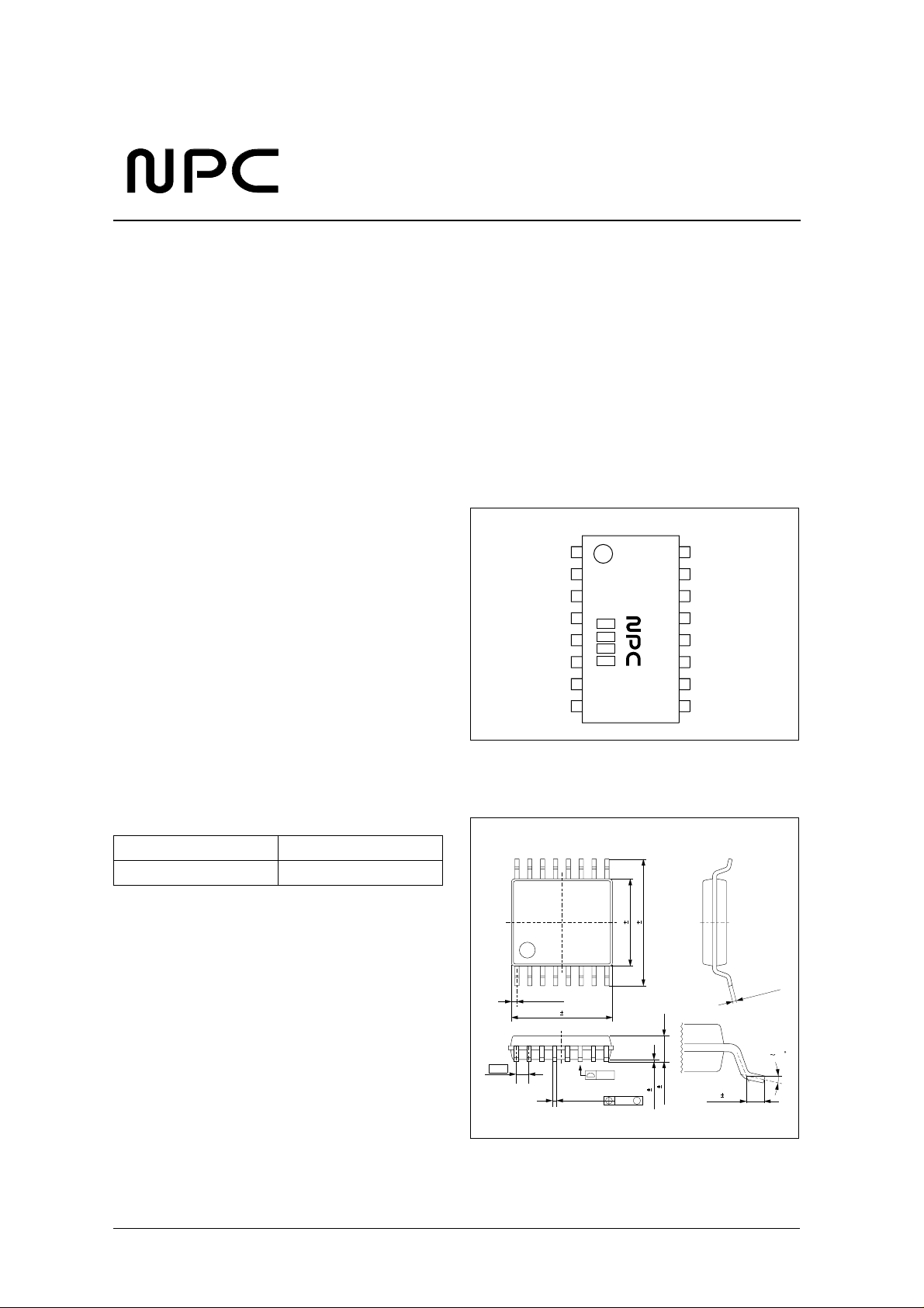
be used to control the EL driver ON/OFF function. The device is available in 16-pin VSOP packages.
FEATURES
■
Dedicated EL driver
■
1.6 to 5.5 V supply voltage
■
150mA maximum operating current
(V
= 3.0V, Ta ≤ 70 ° C)
DD
■
3.5 Ω typical output resistance
■
200 Vp-p maximum EL driver voltage*
■
31 to 1500 Hz EL drive frequency range*
■
High voltage CMOS Process
■
16-pin VSOP plastic package
*: Adjustable with external resistance.
APPLICATIONS
■
Hand held PC, Palm size PC
■
Mobile IT equipment
■
White EL
PINOUT
(Top view)
N.C.
CHV
N.C.
1
16
8143AV
LDR
N.C.
VSS
N.C.
8
OCL OCE
9
PACKAGE DIMENSIONS
(Unit : mm)
N.C.
OUT1
N.C.
OUT2
N.C.
VDD
ENA
ORDERING INFORMATION
De vice Pack ag e
SM8143AV 16-pin VSOP
0.65
0.275TYP
5.1 0.2
4.4 0.2
6.4 0.2
0.10
+ 0.10
0.22
- 0.05
M
0.12
0.10 0.05
NIPPON PRECISION CIRCUITS—1
1.15 0.1
0.5 0.2
0.15
+ 0.1
- 0.05
010
Page 2
.
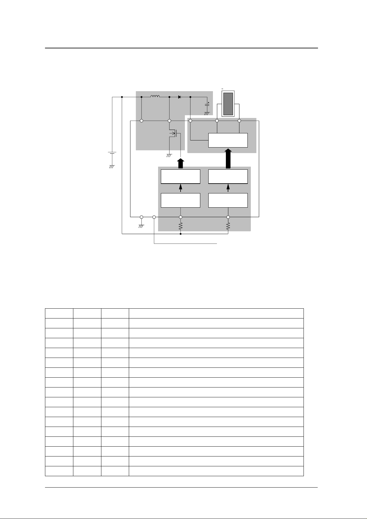
BLOCK DIAGRAM
SM8143A
EL sheet
<
80cm
VDD CHVLDR OUT2OUT1
2
Boosting Block
Switching Circuit
VSS
ENA
Dividing Circuit
1/4
Oscillator for
Boosting
OCL
Dividing Circuit
1/1024
Oscillator for
EL driving
OCE
Oscillation Block
R
OCL ROCE
ENA from microcontroller
When ENA is logical "H", SM8143A is active.
Note: Brightness and operating current are adjusted with R
EL dr iving frequency is adjusted with R
OCE
PIN DESCRIPTION
Pin number Name I / O Function
1 N.C . – No connection (must be open)
2 C H V I High-voltage DC input
3 N.C . – No connection (must be open)
4 LD R O Booster coil driver output
5 N.C . – No connection (must be open)
6 VS S – Ground
7 N.C . – No connection (must be open)
8 OC L I Coil driver oscillator (oscillator frequency determined by external resistor)
9 O CE I E L d river oscillator (oscillator frequency determined by external resistor)
10 ENA I Enable input (built-in pull-down resistor)
11 V DD – Supply
12 N.C . – No connection (must be open)
13 OUT2 O Output 2
14 N.C . – No connection (must be open)
15 OUT1 O Output 1
16 N.C . – No connection (must be open)
OCL
.
NIPPON PRECISION CIRCUITS—2
Page 3

−
≤
≤
=
≤
=
≤
=
≤
=
≤
−
°
°
−
° C
SPECIFICATIONS
Absolute Maximum Ratings
Parameter Symbol Condition Rating Unit
Supply voltage range V
Input voltage range V
Output voltage
Po w er dissipation P
Storage temperature range T
DD
V
CHV
V
LDR
V
OUT1/2
STG
IN
D
−
°
°
°
°
°
SM8143A
0.3 to 7.0 V
All Input pins V
CHV pin 0.5 to 120 V
LDR pin 0.5 to 120 V
OUT1, OUT2 pin 0.5 to 120 V
T
70
C 200 m W
a
T
85
C 140 m W
a
SS
0.3 to V
55 to 125
+ 0.3 V
DD
Recommended Operating Conditions
Parameter Symbol Condition
Supply voltage range V
Operating temperature T
Operating current
1
Coil inductance L
1. Max value is as same as Absolute Maximum Ratings.
DD2
OPR
I
DD2
LDR
Including coil current, V
Including coil current, V
Including coil current, V
Including coil current, V
f
= 64 kHz – 0.47 – m H
LDR
DD
DD
DD
DD
3.0V, T
5.0V, T
3.0V, T
5.0V, T
Rating
min typ max
1.6 3.0 5.5 V
40 – 85
70
C – – 150 mA
a
70
C – – 100 mA
a
85
C – – 105 mA
a
85
C– – 70 mA
a
Unit
C
NIPPON PRECISION CIRCUITS—3
Page 4

DC Characteristics
V
= 3.0 V, T
DD
= 25 ° C unless otherwise noted.
a
SM8143A
Ω
Ω
Ω
Ω
Ω
µ
µ
µ
Parameter Symbol Condition
Supply voltage V
CHV output voltage V
OUT1, OUT2 HIGH-level output voltage V
OUT1, OUT2 LOW-level output voltage V
LDR output resistance R
OCE oscillator frequency f
OCE oscillator frequency range f
OCL oscillator frequency f
OCL oscillator frequency range f
OUT1, OUT2 output frequency f
OUT1, OUT2 output frequency range f
LDR inductance driver frequency f
LDR inductance driver frequency range f
ENA HIGH-level input voltage V
ENA LOW-level input voltage V
ENA input current I
ENA rise time
1
Operating current I
Stand-by current I
1.
DD
CHV
OUTH
OUTL
LDR
OCE1
OCE2
OCL1
OCL2
OUT1
OUT2
LDR1
LDR2
ENAH
ENAL
ENAH
t
ENA
DD1
STB
Rating
Unit
min typ max
1.6 3.0 5.5 V
0.5 – 100 V
– – 100 V
– – 0.5 V
I
= 50 mA – 3.5 5.25
LDR
R
OCE
= 180 k
205 256 307
kHz
32 – 1536
R
OCL
= 180 k
205 256 307
kHz
32 – 1536
R
OCE
= 180 k
200 250 300
Hz
31 – 1500
R
OCL
= 180 k
51 64 77
kHz
8 – 384
ENA = HIGH, V
ENA = LOW, V
V
= V
ENAH
= 1.6 to 5.5V V
DD
= 1.6 to 5.5V V
DD
= 3.0V 2.0 4.0 6.0
DD
– 0.5 – V
DD
– 0.3 – V
SS
DD
SS
+ 0.3
+ 0.5
– – 100
Excluding coil current – – 1. 0 mA
ENA = LOW – – 1.0
V
A
s
A
ENA
VSS
SS + 0.5
V
VDD − 0.5
VDD
tENA
NIPPON PRECISION CIRCUITS—4
Page 5

TYPICAL APPLICATIONS
■
EL sheet size: 20 to 30cm
2
, Current consumption: 20mA
SM8143A
■
EL sheet size: 30 to 50cm
0.1µF
100V
3.0V
470µH
180kΩ
0.01µF
Diode: TOSHIBA 1SS250
Coil: MURATA LQH4N471K04M00
2
, Current consumption: 40mA
0.1µF
100V
3.0V
470µH
360kΩ
0.01µF
N.C.
CHV
N.C.
LDR
N.C.
VSS
N.C.
OCL
N.C.
CHV
N.C.
LDR
N.C.
VSS
N.C.
OCL
N.C.
OUT1
N.C.
OUT2
N.C.
VDD
ENA
OCE
N.C.
OUT1
N.C.
OUT2
N.C.
VDD
ENA
OCE
EL sheet
180kΩ
EL sheet
180kΩ
Diode: TOSHIBA 1SS250
Coil: MURATA LQH4N471K04M00
■
EL sheet size: 50 to 100cm
2
, Current consumption: 80mA
0.1µF
100V
3.0V
330µH
510kΩ
0.01µF
N.C.
CHV
N.C.
LDR
N.C.
VSS
N.C.
OCL
N.C.
OUT1
N.C.
OUT2
N.C.
VDD
ENA
OCE
EL sheet
180kΩ
Diode: TOSHIBA 1SS250
Coil: TOKO D73LC (817CE331M)
Note: Do not operate the SM8143A with the EL sheet NOT connected (no load to OUT1/OUT2) since the IC will be damaged.
NIPPON PRECISION CIRCUITS—5
Page 6

SM8143A
NIPPON PRECISION CIRCUITS INC. reserves the right to make changes to the products described in this data sheet in order to
improve the design or performance and to supply the best possible products. Nippon Precision Circuits Inc. assumes no responsibility for
the use of any circuits shown in this data sheet, conveys no license under any patent or other rights, and makes no claim that the circuits
are free from patent infringement. Applications for any devices shown in this data sheet are for illustration only and Nippon Precision
Circuits Inc. makes no claim or warranty that such applications will be suitable for the use specified without further testing or modification.
The products described in this data sheet are not intended to use for the apparatus which influence human lives due to the failure or
malfunction of the products. Customers are requested to comply with applicable laws and regulations in effect now and hereinafter,
including compliance with export controls on the distribution or dissemination of the products. Customers shall not export, directly or
indirectly, any products without first obtaining required licenses and approvals from appropriate government agencies.
NIPPON PRECISION CIRCUITS INC.
4-3, Fukuzumi 2-chome
Koto-ku, To kyo 135-8430, Japan
NIPPON PRECISION CIRCUITS INC.
Telephone: 03-3642-6661
Facsimile: 03-3642-6698
NC9923AE 2000.05
NIPPON PRECISION CIRCUITS—6
 Loading...