

Page 1
=
P −
SM8140A
NIPPON PRECISION CIRCUITS INC.
OVERVIEW
The SM8140A is designed for using as EL (Electronic Luminescence) sheet driver require very low
external parts counts, this result that very compact
and thin EL driver units can be made.
Also this device has the features to use in wider
range of applications demanding low quiescent current, low supply voltages, low operating supply currents, simple brightness control and low EMI
(Electro-Magnetic Interference) emission due to the
inherent smooth driver wave forms.
FEATURES
■
Specially providing EL driver functions
■
Non-transformer for compact outline
■
Bipolar driving for high power efficiency
■
Very low noise smooth driver wave forms
■
Brightness control with driving frequency change
(An external resistance determines the driving frequency)
■
Low power consumption by quiescent current
control
■
ON-chip high voltage output MOS transistor
■
Large EL sheet (Exceeding 100 cm
■
supply voltage
V
2.4V to 3.6V or 5.0V
DD
■
1.5V and 3V power applicable
2
) drivable
(Refer to APPLICATION HINTS)
■
Maximum output driver voltage:200V
■
Typical driver frequency:250Hz
■
14 pin SSOP
■
chip form
P
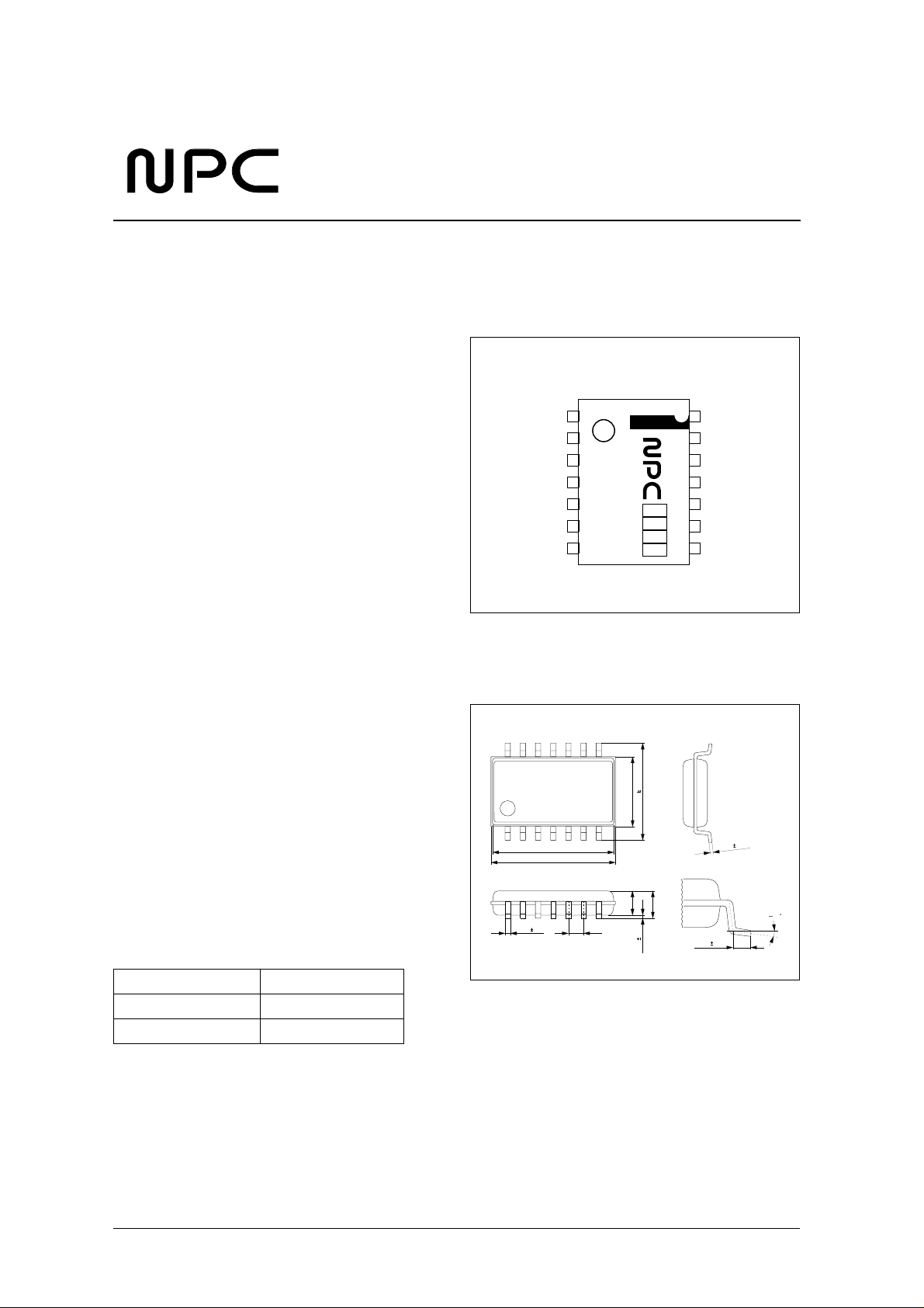
ORDERING INFOMATION
PIN OUT
( Top View )
CHV
LDR
VSS1
OCL2
OCL1
OCE2
OCEl
PIN OUT
( Unit : mm )
8.00
8.20
14pin SSOP
1
SM8140AM
4.40
6.40 0.30
1.50
1.000.35 0.10
1.80MAX
0.10 0.10
EL Driver IC
14
OUT1
OUT2
CP2
CP1
CPO
VDD
87
ENA
0.17 0.20
010
0.625 0.20
Device Package
SM8140AM 14pin SSOP
CF8140A Chip in tray
NIPPON PRECISION CIRCUITS—1
Page 2
SM8140A
PAD DIMENSIONS
( UNIT: µ m )
14
15
16
Y
(0, 0)
Chip size : 2.50 × 2.70mm
Chip thickness : 4000 ± 30 µ m
Pad size : 100 × 100 µ m
Chip reverse side : V
123 4
X
SS
PAD COORDINATES
No. NAME X Y
1 OCE2 360 190
(2500, 2700)
910111213
8
7
6
5
2 OCE1 900 190
3 ENA 1440 190
4 VSS2 2080 190
5 VDD 2310 320
6 CPO 2310 560
7 CP1 2310 1100
8 CP2 2310 1640
9 OUT2 2300 2530
10 OUT1 2100 2530
11 CHV 1900 2530
12 MONG 1700 2530
13 LDR 1500 2530
14 VSS1 190 1600
15 OCL2 190 1040
16 OCL1 190 500
Note : MONG is test pin.
MONG and VSS2 are not bonding.
NIPPON PRECISION CIRCUITS—2
Page 3

BLOCK DIAGRAM
−
−
−
−
SM8140A
ENA
CPO
CP1
CP2
VDD
Enable Circuit
Charge Pump
Circuit
VSS1
(MONG)
Oscillation Circuit
for Voltage Booster
VSS2
Divider
OCL1
LDR
CHV
Level Shifter
OCL2
OUT1
High Voltage
Switching Circuit
Divider
Oscillasion Circuit
for output
OCE1
PIN DESCRIPTION
SSOP chip Pin Name i / o Function
1 11 CHV i DC high voltage pin
12 MONG o Monitor gate
2 13 LDR o Step − up inductor driver output
3 14 VSS1
4 VSS2
4 15 OCL2 o
6 1 OCE2 i CR oscillator pin for output
7 2 OCE1 o External resistor at this pin determines oscillator frequency
8 3 ENA ip
9 5 VDD
10 6 CPO o Charge pump output (Voltage output for driving high voltage MOS)
11 7 CP1 o Charge pump external capacitor pin
12 8 CP2 o Charge pump external capacitor pin
13 9 OUT2 o Output for EL
14 10 OUT1 o Output for EL
GND
GND
CR oscillator pin for step − up inductor and charge pump.
External resistor at this pin determines oscillator frequency.5 16 OCL1 i
1
Output control pin. Output from OUT1 and OUT2 pins are stopped When "L".
−
Power supply pin
OUT2
OCE2
1. "ip" defines input pin with pull down internal resistor
NIPPON PRECISION CIRCUITS—3
Page 4

mH
≤
=
=
=
=
ABSOLUTE MAXIMUM RATINGS
V
0V, Unless otherwise noted
SS
Parameter Symbol Condition Rating unit
Supply voltage range V
Input voltage range V
Output voltage
Power dissipation P
Storage temperature range T
Soldering temperature T
Soldering time t
DD
IN
V
CHV
V
LDR
V
OUT1
V
OUT2
D
STG
SLD
SLD
=
=
=
−
−
−
SM8140A
0.3 to + 8.0 V
All input pins V
CHV pins 0.5 to 120
LDR pins 0.5 to 120
OUT1 pins 0.5 to 120
OUT2 pins 0.5 to 120
Ta ≤ 70 ° C 200 mW
Package only 255
Package only 10 sec
− 0.3 to V
SS
55 to 125
+ 0.3 V
DD
−
−
−
−
Ω
V
° C
° C
RECOMMENDED OPERATING CONDITIONS
V
0V, Unless otherwise noted
SS
Parameter Symbol Condition
V
Supply voltage range
Operating temperature range T
Operating current
2
Using inductor
V
L
L
OPR
I
DD2
I
DD3
LDR1
LDR2
DD1
DD2
CPO = V
1
DD
Including inductor current, V
Including inductor current, V
f
= 32kHz, V
LDR
f
= 32kHz, V
LDR
DD
DD
= 3.0V
= 5.0V
1. 5V Application hints is different from 3V ones (Refer to APPLICATION HINTS)
2. Max value is as same as Absolute Maximum Ratings
ELECTRICAL CHARACTERISTICS
Ta = 25 ° C, V
Parameter Pin Symbol Condition
Supply voltage range VDD V
Output voltage
Output resistance LDR R
Oscillation frequency
Driving frequency OUT1/2 f
Output frequency LDR f
Input voltage ENA
Input current ENA I
Operating current VDD I
Stand − by current VDD I
1. R
determines EL driver frequency 20k to 100kHz
OSC
2. R
determines EL driver frequency 200 to 500Hz
OSC
SS
0V, V
3.0V, unless otherwise noted
DD
DD
CPO V
CHV V
OUT1/2 V
OUT1/2 V
OCE1/2 f
OCL1/2 f
V
V
CPO
CHV
OUTH
OUTL
LDR
OCE
OCL
OUT
LDR
ENAH
ENAL
ENAH
DD1
STB
Excluding inductor current −−1mA
V
2 × V
CPO
V
CPO
R
3.9M Ω
OCE
R
100k Ω
OCL
R
= 3.9MΩ
OCE
R
= 100kΩ 22.4 32 41.6 kHz
OCL
ENA = "H" VDD + 1.0 − VDD + 0.3
ENA = "L" VSS − 0.3 − VSS + 1.0
V
= 3.0V 0.45 0.75 1.05 µA
ENAH
ENA = "L" −−1 µA
DD
DD
6.0V
= 3.0V
= 5.0V
DD
1
2
Rating
min typ max
2.4
4.5
30
−
−
−
−
−
−
−
3.6 V
5.5 V
70
20 100 mA
25 100 mA
1.0
1.5
−
−
Rating
min typ max
2.4
3.6 V
4.5 5.5
0.5
100
−− 100
−− 0.5
5.0 10.0
5.6 8.0 10.4
179 256 332
175 250 325 Hz
unit
° C
mH
unit
V
kHz
V
NIPPON PRECISION CIRCUITS—4
Page 5

APPLICATION HINTS
SM8140A
0.1µF
100V
+
1.0mH
0.1µF
100V
+
0.47mH
1.0kΩ
100kΩ
3.9MΩ
1.0kΩ
100kΩ
CHV
LDR
VSS1
OCL2
OCL1
OCE2
OCEl
CHV
LDR
VSS1
OCL2
OCL1
OCE2
OUT1
OUT2
SM8140AM
CP2
CP1
CPO
VDD
ENA
OUT1
OUT2
SM8140AM
CP2
CP1
CPO
VDD
510Ω
510Ω
EL sheet : SPI ULTRA−THIN TYPE
+
EL sheet size : 10 to 20cm
Current consumption : 20mA (typ.)
470pF
0.01µF
3.0V
Diode : TOSHIBA 1SS250
Coil : MURATA LQH4N102K04M00
EL sheet
EL sheet : SPI ULTRA−THIN TYPE
+
EL sheet size : 20 to 40cm
Current consumption : 40mA (typ.)
470pF
0.01µF
EL sheet
2
+
2
+
100V
+
0.47mH
1.5V
3.9MΩ
1.0kΩ
100kΩ
3.9MΩ
OCEl
CHV
LDR
VSS1
OCL2
OCL1
OCE2
OCEl
ENA
OUT1
OUT2
SM8140AM
CP2
CP1
CPO
VDD
ENA
510Ω
+
EL sheet0.1µF
EL sheet : SPI ULTRA−THIN TYPE
EL sheet size : 10 to 20cm
Current consumption : 20mA (typ.)
470pF
3.0V
Diode : TOSHIBA 1SS250
Coil : MURATA LQH4N471K04M00
0.01µF
+
3.0V
Diode : TOSHIBA 1SS250
Coil : MURATA LQH4N471K04M00
NIPPON PRECISION CIRCUITS—5
Page 6

SM8140A
+
100V
+
0.33mH
100V
1.5mH
1.0kΩ
100kΩ
3.9MΩ
1.0kΩ
36kΩ
3.9MΩ
CHV
LDR
VSS1
OCL2
OCL1
OCE2
OCEl
CHV
LDR
VSS1
OCL2
OCL1
OCE2
OCEl
OUT1
OUT2
SM8140AM
OUT1
OUT2
SM8140AM
CP2
CP1
CPO
VDD
ENA
CP2
CP1
CPO
VDD
ENA
510Ω
EL sheet : SPI ULTRA−THIN TYPE
EL sheet size : 40 to 60cm
Current consumption : 25mA (typ.)
Diode : TOSHIBA 1SS250
Coil : MURATA LQH4N152K04M00
510Ω
EL sheet : SPI ULTRA−THIN TYPE
EL sheet size : 60 to 80cm
Current consumption : 45mA (typ.)
EL sheet0.1µF
5.0V
Diode : TOSHIBA 1SS250
Coil : MURATA LQH4N331K04M00
EL sheet0.1µF
5.0V
100V
+
0.47mH
1.0kΩ
68kΩ
3.9MΩ
CHV
LDR
VSS1
OCL2
OCL1
OCE2
OCEl
OUT1
OUT2
SM8140AM
CP2
CP1
CPO
VDD
ENA
510Ω
EL sheet : SPI ULTRA−THIN TYPE
EL sheet size : 80 to 100cm
Current consumption : 55mA (typ.)
EL sheet0.1µF
5.0V
Diode : TOSHIBA 1SS250
Coil : TOKO 817CE471M
NIPPON PRECISION CIRCUITS INC. reserves the right to make changes to the products described in this data sheet in order to
improve the design or performance and to supply the best possible products. Nippon Precision Circuits Inc. assumes no responsibility for
the use of any circuits shown in this data sheet, conveys no license under any patent or other rights, and makes no claim that the circuits
are free from patent infringement. Applications for any devices shown in this data sheet are for illustration only and Nippon Precision
Circuits Inc. makes no claim or warr anty that such applications will be suitab le for the use specified without further testing or modification.
The products described in this data sheet are not intended to use for the apparatus which influence human lives due to the failure or
malfunction of the products. Customers are requested to comply with applicable laws and regulations in effect now and hereinafter,
including compliance with export controls on the distribution or dissemination of the products. Customers shall not expor t, directly or
indirectly, any products without first obtaining required licenses and approvals from appropriate government agencies..
NIPPON PRECISION CIRCUITS INC.
4-3, 2-chome Fukuzumi
Koto-ku, Tokyo 135-8430, Japan
NIPPON PRECISION CIRCUITS INC.
Telephone: 03-3642-6661
Facsimile: 03-3642-6698
NC9612CE 1998.03
NIPPON PRECISION CIRCUITS—6
 Loading...