

Page 1

SM7320ESQG
®
Dual N-Channel Enhancement Mode MOSFET
Features
• Channel 1
30V/64A,
R
= 5.2mΩ (max.) @ VGS = 10V
DS(ON)
R
= 7.5mΩ (max.) @ VGS = 4.5V
DS(ON)
• Channel 2
30V/85A,
R
= 1.8mΩ (max.) @ VGS =10V
DS(ON)
R
= 2.5mΩ (max.) @ VGS =4.5V
DS(ON)
• 100% UIS + R
Tested
g
• Reliable and Rugged
• Lead Free Available (RoHS Compliant)
Applications
• Power Management in Desktop Computer or
DC/DC Converters.
Pin Description
S2
S2
S2
G2
D1
D1
D1
G1
DFN5x6D-8_EP2
(2)D1(3)
(4)
G1
G2
(8)
N-Channel MOSFET
(1)
2
D
/
1
S
)
9
n
i
P
(
1
D
Pin1
S1/D2
(5)
(6)(7)
S2
Ordering and Marking Information
SM7320ES
Assembly Material
Handling Code
Temperature Range
Package Code
SM7320ES QG :
SM7320
XXXXX
Note : SINOPOWER lead-free products contain molding compounds/die attach materials and 100% matte tin plate
termination finish; which are fully compliant with RoHS. SINOPOWER lead-free products meet or exceed the leadfree requirements of IPC/JEDEC J-STD-020D for MSL classification at lead-free peak reflow temperature. SINOPOWER
defines “Green” to mean lead-free (RoHS compliant) and halogen free (Br or Cl does not exceed 900ppm by weight
in homogeneous material and total of Br and Cl does not exceed 1500ppm by weight).
SINOPOWER reserves the right to make changes to improve reliability or manufacturability without notice, and
advise customers to obtain the latest version of relevant information to verify before placing orders.
Copyright Sinopower Semiconductor, Inc.
Rev. A.5 - July, 2015
Package Code
QG : DFN5x6D-8_EP2
Operating Junction Temperature Range
C : -55 to 150 oC
Handling Code
TR : Tape & Reel
Assembly Material
G : Halogen and Lead Free Device
XXXXX - Lot Code
www.sinopowersemi.com1
Page 2

SM7320ESQG
C).
®
Absolute Maximum Ratings (T
Symbol
Parameter Channel 1 Channel 2 Unit
= 25°C unless otherwise noted)
A
Common Ratings
V
Drain-Source Voltage
DSS
V
Gate-Source Voltage
GSS
TJ
Maximum Junction Temperature
T
Storage Temperature Range
STG
30
±20
150 °C
-55 to 150 °C
IS Diode Continuous Forward Current 30 75 A
b
I
I
Pulse Drain Current Tested 200 300 A
DP
a
Continuous Drain Current
D
TC=25°C 64 85
TC=100° C 40 80
PD
Maximum Power Dissipation
TC=25°C 35 83
TC=100° C 14 33
R
Thermal Resistance-Junction to Case Steady State
θJC
3.5 1.5 °C/W
TA=25°C 16 30
ID
Continuous Drain Current
TA=70°C 13 24
V
V
A
W
A
PD
Maximum Power Dissipation
TA=25°C 2.08 2.38
W
TA=70°C 1.33 1.52
R
Thermal Resistance-Junction to Ambient
θJA
t ≤ 10s
Steady State
c
I
AS
E
Note a:Package is limited to 85A.
Note b:Pulse width is limited by max. junction temperature.
Note c: UIS tested and pulse width are limited by maximum junction temperature 150oC(initial temperature Tj=25
Avalanche Current, Single pulse (L=0.1mH) 30 50 A
c
Avalanche Energy, Single pulse (L=0.1mH) 45 125 mJ
AS
30 28
°C/W
60 52.5
o
Copyright Sinopower Semiconductor, Inc.
Rev. A.5 - July, 2015
www.sinopowersemi.com2
Page 3

SM7320ESQG
®
Channel 1 Electrical Characteristics (T
= 25°C unless otherwise noted)
A
Channel 1
Symbol
Parameter Test Conditions
Min. Typ. Max.
Static Characteristics
BV
Drain-Source Breakdown Voltage
DSS
VGS=0V, IDS=250µA
30 - - V
VDS=24V, VGS=0V - - 1
I
Zero Gate Voltage Drain Current
DSS
V
Gate Threshold Voltage
GS(th)
I
Gate Leakage Current VGS=±20V, VDS=0V - - ±100 nA
GSS
VDS=VGS, IDS=250µA
TJ=85°C
- - 30
1.5 1.8 2.5 V
VGS=10V, IDS=20A - 4.3 5.2
DS(ON)
d
Drain-Source On-state Resistance
TJ=125°C - 6 - R
VGS=4.5V, IDS=15A - 5.7 7.5
Gfs Forward Transconductance VDS=5V, IDS=15A - 30 - S
Diode Characteristics
d
V
Diode Forward Voltage ISD=10A, VGS=0V - 0.75 1.1 V
SD
trr Reverse Recovery Time - 17.1
ta Charge Time - 9.4 -
IDS=5A, dlSD/dt=100A/µs
tb Discharge Time - 7.7 -
Qrr Reverse Recovery Charge
- 9.3 - nC
Unit
µA
mΩ
ns
Dynamic Characteristics e
RG Gate Resistance VGS=0V,VDS=0V,F=1MHz 0.4 0.6 1.5
C
Input Capacitance 1160 1450 1740
iss
C
Output Capacitance 181 258 335
oss
C
Reverse Transfer Capacitance
rss
t
Turn-on Delay Time - 10 19
d(ON)
tr Turn-on Rise Time - 11 21
t
Turn-off Delay Time - 25 46
d(OFF)
tf Turn-off Fall Time
VGS=0V,
VDS=15V,
Frequency=1.0MHz
VDD=15V, RL=15Ω,
IDS=1A, V
GEN
=10V,
RG=6Ω
80 133 186
- 8 15
Gate Charge Characteristics e
Qg Total Gate Charge
VDS=15V, VGS=4.5V,
IDS=20A
- 12.5
Qg Total Gate Charge - 26.2 37
Q
Threshold Gate Charge - 1.9 -
gth
Qgs Gate-Source Charge - 3.2 Qgd Gate-Drain Charge
Note d:Pulse test ; pulse width≤300µs, duty cycle≤2%.
Note e:Guaranteed by design, not subject to production testing.
VDS=15V, VGS=10V,
IDS=20A
- 5.6 -
Ω
pF
ns
-
nC
Copyright Sinopower Semiconductor, Inc.
Rev. A.5 - July, 2015
www.sinopowersemi.com3
Page 4

SM7320ESQG
®
Channel 2 Electrical Characteristics (T
= 25°C unless otherwise noted)
A
Channel 2
Symbol
Parameter Test Conditions
Min. Typ. Max.
Static Characteristics
BV
Drain-Source Breakdown Voltage
DSS
VGS=0V, IDS=250µA
30 - - V
VDS=24V, VGS=0V - - 1
I
Zero Gate Voltage Drain Current
DSS
V
Gate Threshold Voltage
GS(th)
I
Gate Leakage Current VGS=±20V, VDS=0V - - ±100 nA
GSS
VDS=VGS, IDS=250µA
TJ=85°C
- - 30
1.4 1.7 2.5 V
VGS=10V, IDS=30A - 1.5 1.8
DS(ON)
d
Drain-Source On-state Resistance
TJ=125°C - 2 - R
VGS=4.5V, IDS=15A - 1.9 2.5
Gfs Forward Transconductance VDS=5V, IDS=15A - 37 - S
Diode Characteristics
d
V
Diode Forward Voltage ISD=20A, VGS=0V - 0.75 1.1 V
SD
trr Reverse Recovery Time - 31.4
ta Charge Time - 14.7
IDS=30A, dlSD/dt=100A/µs
tb Discharge Time - 16.7
Qrr Reverse Recovery Charge
- 22.9
Dynamic Characteristics e
Unit
µA
mΩ
-
-
ns
-
- nC
RG Gate Resistance VGS=0V,VDS=0V,F=1MHz 0.5 0.7 1.5
C
Input Capacitance 3160 3950 4938
iss
C
Output Capacitance 602 860 1118
oss
C
Reverse Transfer Capacitance
rss
t
Turn-on Delay Time - 18 33
d(ON)
tr Turn-on Rise Time - 12 23
t
Turn-off Delay Time - 47 86
d(OFF)
tf Turn-off Fall Time
VGS=0V,
VDS=15V,
Frequency=1.0MHz
VDD=15V, RL=15Ω,
IDS=1A, V
GEN
=10V,
RG=6Ω
237 395 572
- 27 50
Gate Charge Characteristics e
Qg Total Gate Charge
VDS=15V, VGS=4.5V,
IDS=30A
- 29.9
Qg Total Gate Charge - 65.2 91
Q
Threshold Gate Charge - 4.8 -
gth
Qgs Gate-Source Charge - 8.6 Qgd Gate-Drain Charge
Note d:Pulse test ; pulse width≤300µs, duty cycle≤2%.
Note e:Guaranteed by design, not subject to production testing.
VDS=15V, VGS=10V,
IDS=30A
- 13 -
Copyright Sinopower Semiconductor, Inc.
Rev. A.5 - July, 2015
www.sinopowersemi.com4
Ω
pF
ns
-
nC
Page 5

SM7320ESQG
Channel 1 Typical Operating Characteristics
®
Power Dissipation
40
35
30
25
20
Ptot - Power (W)
15
10
5
TC=25oC
0
0 20 40 60 80 100120140160
Tj - Junction Temperature (° C)
Safe Operation Area
500
Drain Current
70
60
50
40
30
20
ID - Drain Current (A)
10
TC=25oC,VG=10V
0
0 20 40 60 80 100120140160
Tj - Junction Temperature (°C)
Thermal Transient Impedance
4
100
100µs
Rds(on) Limit
10
ID - Drain Current (A)
1
TC=25oC
0.1
0.01 0.1 1 10 100300
1ms
10ms
DC
VDS - Drain - Source Voltage (V)
Copyright Sinopower Semiconductor, Inc.
Rev. A.5 - July, 2015
1
0.1
0.01
1E-3
0.01
0.05
0.02
Single Pulse
Normalized Transient Thermal Resistance
1E-4
1E-6 1E-5 1E-4 1E-3 0.01 0.1
Square Wave Pulse Duration (sec)
0.1
0.2
www.sinopowersemi.com5
Duty = 0.5
R
:3.5oC/W
θJC
Page 6

SM7320ESQG
Channel 1 Typical Operating Characteristics (Cont.)
®
Output Characteristics
140
120
100
80
60
40
ID - Drain Current (A)
20
0
0.0 0.5 1.0 1.5 2.0 2.5 3.0
VGS=5,6,7,8,9,10V
4V
3.5V
3V
2.5V
VDS - Drain - Source Voltage (V)
Gate-Source On Resistance
30
25
20
IDS=20A
Drain-Source On Resistance
12
10
8
VGS=4.5V
6
4
2
RDS(ON) - On - Resistance (mΩ)
0
0 20 40 60 80 100 120
VGS=10V
ID - Drain Current (A)
Gate Threshold Voltage
1.6
1.4
1.2
1.0
IDS=250µA
15
10
RDS(ON) - On - Resistance (mΩ)
5
0
2 3 4 5 6 7 8 9 10
VGS - Gate - Source Voltage (V)
Copyright Sinopower Semiconductor, Inc.
Rev. A.5 - July, 2015
0.8
0.6
0.4
Normalized Threshold Vlotage
0.2
0.0
-50 -25 0 25 50 75 100125150
Tj - Junction Temperature (° C)
www.sinopowersemi.com6
Page 7

SM7320ESQG
Channel 1 Typical Operating Characteristics (Cont.)
®
Drain-Source On Resistance
1.8
VGS = 10V
IDS = 20A
1.6
1.4
1.2
1.0
0.8
Normalized On Resistance
0.6
RON@Tj=25oC: 4.3mΩ
0.4
-50 -25 0 25 50 75 100125150
Tj - Junction Temperature (°C)
2000
1750
1500
1250
Capacitance Gate Charge
Frequency=1MHz
Ciss
Source-Drain Diode Forward
200
100
10
1
Tj=150oC
Tj=25oC
IS - Source Current (A)
0.1
0.0 0.2 0.4 0.6 0.8 1.0 1.2 1.4
VSD - Source - Drain Voltage (V)
10
VDS= 15V
9
IDS= 20A
8
7
6
1000
750
C - Capacitance (pF)
500
Crss
250
0
0 5 10 15 20 25 30
VDS - Drain - Source Voltage (V)
Copyright Sinopower Semiconductor, Inc.
Rev. A.5 - July, 2015
Coss
5
4
3
2
VGS - Gate-source Voltage (V)
1
0
0 4 8 12 16 20 24 28
QG - Gate Charge (nC)
www.sinopowersemi.com7
Page 8

SM7320ESQG
Channel 2 Typical Operating Characteristics
®
Power Dissipation
90
75
60
45
Ptot - Power (W)
30
15
TC=25oC
0
0 20 40 60 80 100120140160
Tj - Junction Temperature (° C)
Safe Operation Area
800
Drain Current
100
80
60
40
ID - Drain Current (A)
20
TC=25oC,VG=10V
0
0 20 40 60 80 100120140160
Tj - Junction Temperature (°C)
Thermal Transient Impedance
4
100
Rds(on) Limit
10
ID - Drain Current (A)
1
TC=25oC
0.1
0.01 0.1 1 10 100300
VDS - Drain - Source Voltage (V)
Copyright Sinopower Semiconductor, Inc.
Rev. A.5 - July, 2015
10µs
100µs
1ms
DC
0.2
Duty = 0.5
www.sinopowersemi.com8
R
θJC
:1.5oC/W
1
0.1
0.05
0.1
0.01
0.02
0.01
Single Pulse
Normalized Transient Thermal Resistance
1E-3
1E-6 1E-5 1E-4 1E-3 0.01 0.1
Square Wave Pulse Duration (sec)
Page 9

SM7320ESQG
Channel 2 Typical Operating Characteristics (Cont.)
®
Output Characteristics
160
VGS=3.5,4,5,6,7,8,9,10V
140
120
100
80
60
ID - Drain Current (A)
40
20
0
0.0 0.5 1.0 1.5 2.0 2.5 3.0
3V
2.5V
VDS - Drain - Source Voltage (V)
Gate-Source On Resistance
12
10
IDS=30A
Drain-Source On Resistance
3.5
3.0
2.5
2.0
1.5
1.0
RDS(ON) - On - Resistance (mΩ)
0.5
0.0
0 30 60 90 120 150
VGS=4.5V
VGS=10V
ID - Drain Current (A)
Gate Threshold Voltage
1.6
1.4
IDS =250µA
8
6
4
RDS(ON) - On - Resistance (mΩ)
2
0
2 3 4 5 6 7 8 9 10
VGS - Gate - Source Voltage (V)
Copyright Sinopower Semiconductor, Inc.
Rev. A.5 - July, 2015
1.2
1.0
0.8
0.6
Normalized Threshold Vlotage
0.4
0.2
-50 -25 0 25 50 75 100125150
Tj - Junction Temperature (° C)
www.sinopowersemi.com9
Page 10

SM7320ESQG
Channel 2 Typical Operating Characteristics (Cont.)
®
Drain-Source On Resistance
1.8
VGS = 10V
IDS = 30A
1.6
1.4
1.2
1.0
0.8
0.6
Normalized On Resistance
0.4
0.2
-50 -25 0 25 50 75 100125150
Tj - Junction Temperature (°C)
6000
5000
RON@Tj=25oC: 1.5mΩ
Capacitance Gate Charge
Frequency=1MHz
Source-Drain Diode Forward
100
10
1
Tj=150oC
Tj=25oC
IS - Source Current (A)
0.1
0.0 0.2 0.4 0.6 0.8 1.0 1.2
VSD - Source - Drain Voltage (V)
10
VDS= 15V
9
IDS= 30A
8
4000
3000
2000
Ciss
C - Capacitance (pF)
1000
Crss
0
0 5 10 15 20 25 30
VDS - Drain - Source Voltage (V)
Copyright Sinopower Semiconductor, Inc.
Rev. A.5 - July, 2015
Coss
7
6
5
4
3
2
VGS - Gate-source Voltage (V)
1
0
0 10 20 30 40 50 60 70
QG - Gate Charge (nC)
www.sinopowersemi.com10
Page 11

SM7320ESQG
Avalanche Test Circuit and Waveforms
VDS
L
DUT
RG
VDD
IAS
®
VDSX(SUS)
tp
VDS
tp
IL
0.01Ω
VDD
Switching Time Test Circuit and Waveforms
VDS
RD
DUT
VGS
RG
VDD
tp
VDS
90%
10%
VGS
td(on) tr
EAS
tAV
td(off) tf
Copyright Sinopower Semiconductor, Inc.
Rev. A.5 - July, 2015
www.sinopowersemi.com11
Page 12
SM7320ESQG
Disclaimer
Sinopower Semiconductor, Inc. (hereinafter “Sinopower”) has been making
great efforts to development high quality and better performance products to
satisfy all customers’ needs. However, a product may fail to meet customer’s
expectation or malfunction for various situations.
All information which is shown in the datasheet is based on Sinopower’s
research and development result, therefore, Sinopower shall reserve the right
to adjust the content and monitor the production.
In order to unify the quality and performance, Sinopower has been following
JEDEC while defines assembly rule. Notwithstanding all the suppliers
basically follow the rule for each product, different processes may cause
slightly different results.
®
The technical information specified herein is intended only to show the typical
functions of and examples of application circuits for the products. Sinopower
does not grant customers explicitly or implicitly, any license to use or exercise
intellectual property or other rights held by Sinopower and other parties.
Sinopower shall bear no responsible whatsoever for any dispute arising from
the use of such technical information.
The products are not designed or manufactured to be used with any
equipment, device or system which requires an extremely high level of
reliability, such as the failure or malfunction of which any may result in a direct
threat to human life or a risk of human injury. Sinopower shall bear no
responsibility in any way for use of any of the products for the above special
purposes. If a product is intended to use for any such special purpose, such
as vehicle, military, or medical controller relevant applications, please contact
Sinopower sales representative before purchasing.
Copyright Sinopower Semiconductor, Inc.
Rev. A.5 - July, 2015
www.sinopowersemi.com12
Page 13
SM7320ESQG
Classification Profile
®
Copyright Sinopower Semiconductor, Inc.
Rev. A.5 - July, 2015
www.sinopowersemi.com13
Page 14

SM7320ESQG
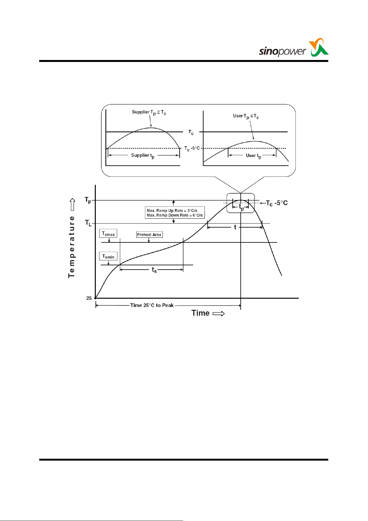
Classification Reflow Profiles
Profile Feature Sn-Pb Eutectic Assembly Pb-Free Assembly
®
Preheat & Soak
Temperature min (T
Temperature max (T
Time (T
smin
to T
smax
smin
smax
) (ts)
)
)
Average ramp-up rate
(T
to TP)
smax
Liquidous temperature (TL)
Time at liquidous (tL)
Peak package body Temperature
(Tp)*
Time (tP)** within 5°C of the specified
classification temperature (Tc)
Average ramp-down rate (Tp to T
smax
Time 25°C to peak temperature
See Classification Temp in table 1 See Classification Temp in table 2
)
100 °C
150 °C
60-120 seconds
150 °C
200 °C
60-120 seconds
3 °C/second max. 3°C/second max.
183 °C
60-150 seconds
217 °C
60-150 seconds
20** seconds 30** seconds
6 °C/second max. 6 °C/second max.
6 minutes max. 8 minutes max.
* Tolerance for peak profile Temperature (Tp) is defined as a supplier minimum and a user maximum.
** Tolerance for time at peak profile temperature (tp) is defined as a supplier minimum and a user maximum.
Table 1. SnPb Eutectic Process – Classification Temperatures (Tc)
Package
Thickness
<2.5 mm
≥2.5 mm 220 °C 220 °C
Table 2. Pb-free Process – Classification Temperatures (Tc)
Package
Thickness
<1.6 mm
1.6 mm – 2.5 mm
Volume mm3
<350
260 °C 260 °C 260 °C
260 °C 250 °C 245 °C
Volume mm
<350
235 °C 220 °C
3
Volume mm3
350-2000
Volume mm
≥350
Volume mm3
3
>2000
≥2.5 mm 250 °C 245 °C 245 °C
Reliability Test Program
Test item Method Description
SOLDERABILITY JESD-22, B102 5 Sec, 245°C
HTRB JESD-22, A108 1000 Hrs, 80% of VDS max @ Tjmax
HTGB JESD-22, A108 1000 Hrs, 100% of VGS max @ Tjmax
PCT JESD-22, A102
TCT JESD-22, A104 500 Cycles, -65° C~150°C
168 Hrs, 100%RH, 2atm, 121°C
Customer Service
Sinopower Semiconductor, Inc.
5F, No. 6, Dusing 1St Rd., Hsinchu Science Park,
Hsinchu, 30078, Taiwan
TEL: 886-3-5635818 Fax: 886-3-5635080
Copyright Sinopower Semiconductor, Inc.
Rev. A.5 - July, 2015
www.sinopowersemi.com14
 Loading...