

Page 1
preliminary
−∆
SM6781BV
NIPPON PRECISION CIRCUITS INC.
Ni-MH/Ni-Cd Battery Charger IC
OVERVIEW
The SM6781BV is a quick charge control IC for Nickel Metal Hydride (NiMH) and Nickel-Cadmium (NiCd)
rechargeable batteries. Quick charging ends in response to negative delta voltage detection (– ∆ V) and maximum charging time detection functions. Also, quick charge mode is placed on hold if the battery voltage
becomes abnormal, until normal conditions are restored. The SM6781BV requires few external components to
realize a high-stability quick charge battery charger.
FEATURES
■
Ni-MH/Ni-Cd battery quick charge control
■
V and maximum charge time cutoffs
■
15min (typ) −∆ V detection invalid time
■
– 4mV (typ) −∆ V detection accuracy
■
Inhibit function
■
Charge condition LED indicator output
(on, pulsed, off)
■
Low power dissipation standby mode (< 1 µ A)
■
8-pin VSOP package
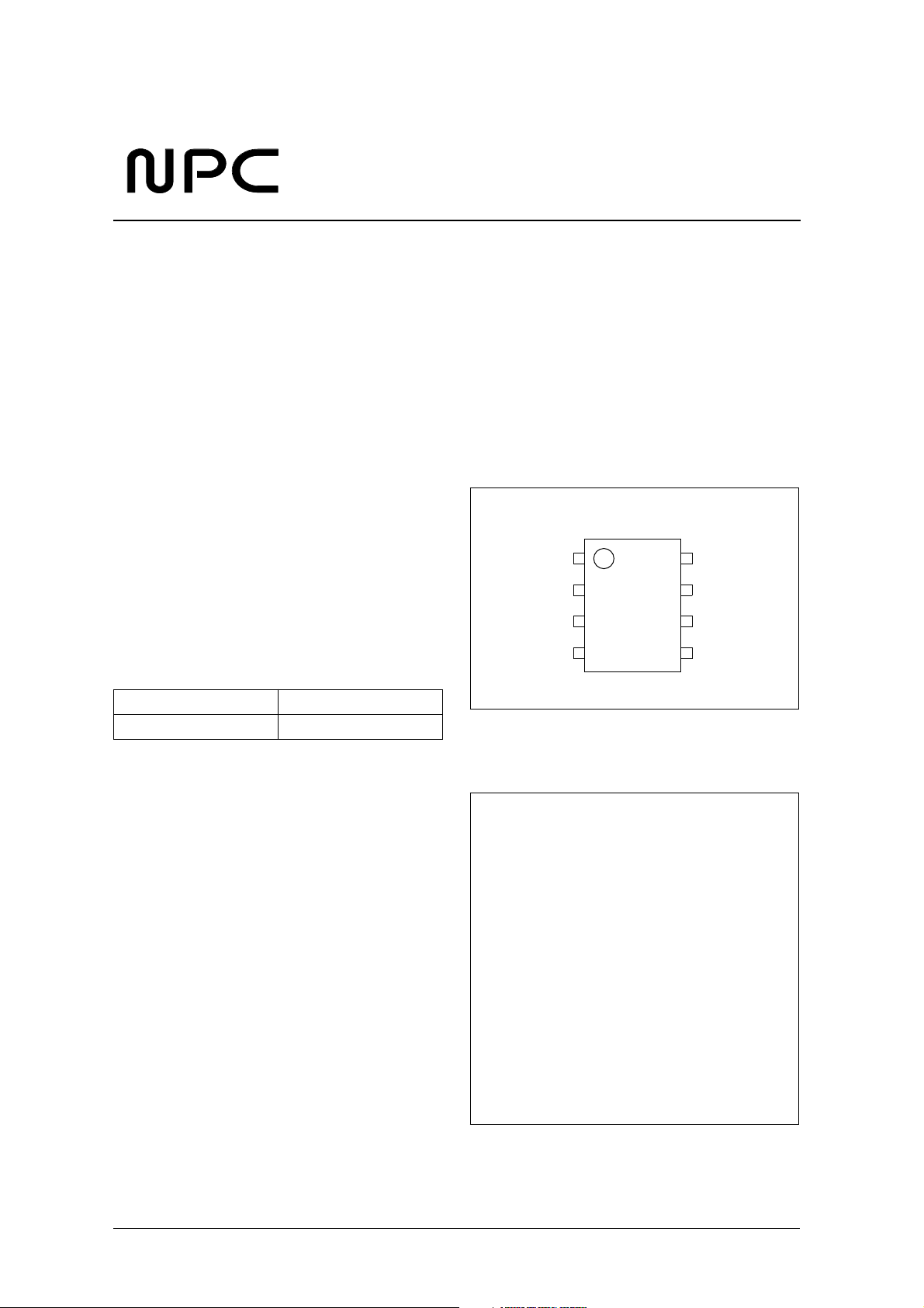
PINOUT
(Top view)
TIME CHGN
LEDN
BATT
INH
NC
ORDERING INFORMATION
Device Package
SM6781BV 8-pin VSOP
VSS
PACKAGE DIMENSIONS
(Unit: mm)
TBD
VDD
NIPPON PRECISION CIRCUITS—1
Page 2
preliminary
BLOCK DIAGRAM
DC
Input
SM6781BV
VDD
TIMEVDD
Current
Source
Battery
Pack
BATT
INH
Reference
Regulators
Max/Min
Cell-voltage
Check
OSC
A/D
−∆V
Function
Block
VSS
Timer Mode
Selector
Timing Control
Charge Control
PIN DESCRIPTION
Number Name I/O Description
1 TIME I
2 LEDN O
3BATT I
4 VSS – Ground
5 VDD – Supply
6 NC – No connection (must be open)
7INH I
8 CHGN O
Timer mode select input (3-level)
HIGH and LOW levels applied using pull-up and pull-down, respectively. MID-level is applied using a
voltage divider resistor network with voltage VDD/2.
Charge status display LED driver output (open-drain output)
LOW-level output in quick charge mode. 1Hz pulse output when abnormal battery voltage is detected
during quick charge. High impedance when charging finishes.
Battery voltage detector input.
Connect a high-impedance resistor voltage divider between the poles of the battery for voltage detection.
Inhibit input
Charging operation is stopped when HIGH. Charging recommences with the same charging parameters
when INH goes LOW again.
Charge control (open-drain output)
High impedance output when charging current is flowing. LOW-level output when charging current stops.
CHGN
CHG Driver
VDD
Logic
LEDN
LED Driver
Logic
NC
NIPPON PRECISION CIRCUITS—2
Page 3
preliminary
−
−
−
°
°
SPECIFICATIONS
Absolute Maximum Ratings
V
= 0V
SS
Parameter Symbol Condition Rating Unit
Supply voltage range V
Input voltage range V
Storage temperature range T
Operating temperature range T
Power dissipation P
DC Characteristics 1
DD
IN
stg
opr
D
−
−
−
−
SM6781BV
0.3 to 7.0 V
0.3 to 7.0 V
55 to 125
– 25 to 85
150 mW
C
C
V
= 4.0 to 5.5V, V
DD
Parameter Symbol Condition Rating Variation Unit
Minimum battery voltage V
Maximum battery voltage V
= 0V, Ta = 25 ° C
SS
DC Characteristics 2
V
= 4.0 to 5.5V, V
DD
Parameter Symbol Condition
VDD supply voltage V
BATT input voltage V
INH HIGH-level input voltage V
INH LOW-level input voltage V
TIME HIGH-level input voltage V
TIME MID-level input voltage V
TIME LOW-level input voltage V
BATT −∆ V detection voltage
range
LEDN output pulse frequency f
BATT standby voltage V
VDD current consumption I
VDD standby current I
LEDN, CHGN sink current I
INH, TIME input leakage
current
LEDN, CHGN output leakage
current
= 0V, Ta = 0 to 85 ° C unless otherwise noted
SS
MNV
MXV
BATT
V
LED
STB
I
DD
IH1
IL1
IH2
IM
IL2
DET
STB
DD
OL
I
OZ
V
< V
BATT
V
BATT
V
= 5V, no load – – 0.5 mA
DD
V
= 5V, V
DD
V
= V
OL
V
L
INH
charge cutoff or prohibition 0.6 ± 0.2 V
MNV
> V
charge cutoff or prohibition 2.0 ± 0.1 V
MXV
Rating
min typ max
4.0 5.0 5.5 V
0–V
0.7 – – V
– – 0.1 V
V
0.5 – – V
DD
(V
/2) − 0.5 – (V
DD
– – 0.5 V
1–2V
–1–Hz
V
1.5 – V
DD
= V
BATT
+ 0.8V 10 – – mA
SS
= V
= V
TIME
, no load – – 1 µA
DD
to V
SS
DD
– – ± 1 µA
5– –µA
DD
/2) + 0.5 V
DD
0.5 V
DD
Unit
V
NIPPON PRECISION CIRCUITS—3
Page 4

preliminary
SM6781BV
Maximum Quick Charging Time
V
= 5V, Ta = 25 ° C
DD
TIME pin min typ max Unit
HIGH 192 240 288 min
MIDDLE 96 120 144 min
LOW 648096min
V Detection Voltage
V
= 5V, Ta = 25 ° C
DD
min typ max Unit
V detection voltage – – 4 – mV
– ∆
– ∆
– ∆
– ∆
V detection prohibit time
V
= 5V, Ta = 25 ° C
DD
min typ max Unit
V detection prohibit time 720 900 1080 sec
NIPPON PRECISION CIRCUITS—4
Page 5

preliminary
FUNCTIONAL DESCRIPTION
Charging Flowchart
Supply applied
Standby mode released
Initialization (approx. 200ms)
SM6781BV
Maximum quick charge time count start
−∆V detection prohibit time count start
Battery voltage check start
(Abnormal battery voltage detection
at V
BATT ≥ 2V or 0.6V > VBATT)
Continuously battery voltage check operation
Quick charge mode
(−∆V detection prohibit condition)
LEDN = LOW (ON)
CHGN = High impedance
NO
−∆V detection prohibit time passed
YES
Quick charge mode
(−∆V detection active condition)
LEDN = LOW (ON)
CHGN = High impedance
− ∆V detection
NO
Maximum quick charge time passed
or
Abnormal battery voltage detection
Abnormal battery voltage
detection cleared
(Return status in force
before abnormal battery
voltage detected)
Abnormal battery voltage detection
Maximum quick charge time count stopped
−∆V detection prohibit time count stopped
Quick charge hold
LEDN = High impedance (pulsing)
CHGN = LOW
(Battery voltage: VBATT ≥ 2V or 0.6V > VBATT)
Maximum quick charge time count restarted
Battery voltage check
CHGN = LOW
(Quick charge current stop condition)
NO
Peak voltage data clear
−∆V detection prohibit time count restarted
YES
YES
Quick charge finished
Battery voltage check stop
LEDN = High impedance (OFF)
CHGN = LOW
Abnormal battery voltage
detection cleared
NIPPON PRECISION CIRCUITS—5
Page 6

preliminary
– ∆
– ∆
SM6781BV
Initialization
The SM6781BV charging operation commences when power is applied or when a battery is inserted (standby
mode released). Approximately 200ms are required when operation starts to initialize all internal circuits.
When initialization finishes, the charging mode is determined by the BATT input voltage and the timer mode.
Battery Voltage Check
When the BATT input voltage is outside the permitted range, quick charge stops. At this point, the maximum
quick charge time count and - ∆ V prohibit time counters also stop. When the BATT input voltage comes back
within the permitted range, quick charge and timer stop conditions are released. When quick charge mode is
restarted, the saved peak voltage data is reset (cleared to 0V).
V Detection Prohibit Time
V detection is not performed for approximately 15 minutes from when quick charge commences (quick
charge cumulative time).
CHGN Output
CHGN becomes high impedance during quick charge. CHGN goes LOW when quick charge mode finishes or
when abnormal battery voltage is detected.
Hi-Z
CHGN
Low
Figure 1. CHGN state
LEDN Output
LEDN is LOW during quick charge (LED is ON), and high impedance after quick charge finishes (LED is
OFF). When an abnormal battery voltage is detected before quick charge finishes, a pulse of approximately
1Hz is output (LED flashes). Also, a 1Hz pulse is output when INH is HIGH.
Hi-Z
LED OFF
Low
Approximately
200ms
Depends on charge mode
Stop/Hold/INH=HighQuick charge
Power ON or Standby mode cancel
Figure 2. LEDN output
Quick Charge Termination
Quick charge finishes when either – ∆ V voltage is detected or the maximum charging time has elapsed.
NIPPON PRECISION CIRCUITS—6
Page 7

preliminary
V Detection Function
SM6781BV
– ∆
– ∆
– ∆
A – ∆ V condition is detected when the BATT voltage (V
voltage, at which point the battery is deemed to be fully charged and quick charge finishes (valid for 1V <
V
< 2V).
BATT
Cell voltage
Quick charge time
Figure 3. Battery voltage change
V Detection A/D Converter
The A/D converter employs double integration A/D conversion, and converts samples taken approximately
every 1.17 seconds.
V Detection Timing
The – ∆ V detection and peak voltage detection are determined by the average value of 16 A/D converted samples. Consequently, – ∆ V detection timing occurs approximately every 18 seconds (16-sample length).
) falls 4mV (typ) or more below the peak battery
BATT
4mV
V
peak
− ∆V detect
490ms max
16 2 3
A/D convert
− ∆V detect
Standby Mode
When the BATT input voltage exceeds the standby voltage V
In this mode, the maximum charging time timer, – ∆ V detection prohibit timer, and peak voltage data are all
reset to zero. At this time, the CHGN and LEDN outputs both become high impedance.
Charge Inhibit (INH)
When INH goes HIGH, charge mode operation stops. While INH is HIGH, the internal timer stops, CHGN
goes LOW and LEDN outputs 1Hz pulse (LEDN flashes). When INH goes LOW, the SM6781BV is restored to
the previous state and the internal timer restarts. If INH is connected to temperature switch (NPC SM6611), it
realizes simple temperature control.
Peak hold
and compare
1
1.17sec
Averaging
18.7sec
Figure 4. – ∆V detection and A/D convert
, the device enters standby mode.
STB
15 16
Peak hold
and compare
Operation
Stop
NIPPON PRECISION CIRCUITS—7
Page 8

preliminary
SM6781BV
BATT Input
The voltage applied to the BATT input, used for battery voltage detection, is a voltage potential, derived by a
voltage divider resistor network (100kΩ or higher recommended) or other means, that represents the voltage of
a single battery cell during charging. If a single cell only is under charge, a current limiting resistor (100kΩ or
higher is recommended) should be connected between the battery and BATT input.
Current
Source
Ra
N
Rb
Figure 5. BATT connection example (multiple)
BATT pin
Ra
= N − 1
Rb
N:Number of cells
Operating Mode vs. BATT Input Voltage
Battery voltage
VDD − 0.5
VDD − 1.5
[V]
2.0
1.0
0.6
Battery
check
0
NG
NG
Current
Source
100kΩ
Figure 6. BATT connection example (single)
Quick
charge
Valid
−∆V
detect
Valid
Standby
mode
Valid
BATT pin
Charging Operating Status
Conditions
Charging status
INH
Quick charge LOW Yes High impedance LOW (ON) Count
Quick charge hold LOW No LOW 1Hz (pulsing) Hold
Quick charge inhibit HIGH – LOW 1Hz (pulsing) Hold
Quick charge finish LOW Yes LOW High impedance (OFF) Reset
Standby – – High impedance High impedance (OFF) Reset
Battery
check OK
CHGN output LEDN output Internal timer
NIPPON PRECISION CIRCUITS—8
Page 9

preliminary
TYPICAL APPLICATION CIRCUIT
SM6781BV
VBB 12V
VDD 5V
SW1
1.8kΩ
R3
100kΩ
R4
100kΩ
R5
R1
5.1kΩ
2SC945
SM6781BV
5
VDD
2
LEDN
1
TIME
4
VSS
Q1
33kΩ
R
9
= N − 1
R10
N= Number of cells
R6
CHGN
INH
NC
BATT
IN
R7
100kΩ
8
7
6
3
78L05
VSS
OUT
5V
Q3
2SC945
R9
200kΩ
R10
200kΩ
VBEQ2
Q2
2SD525
R2
4/5W
ICHG
Temperature switch
5 − V
I
CHG =
=
CPU
or
(SM6611)
BEQ2
R2
5 − 0.65
4
Note that the above circuit is an example circuit to demonstrate the connections for device functions. Battery
charger operation is not guaranteed.
NIPPON PRECISION CIRCUITS—9
Page 10

preliminary
SM6781BV
NIPPON PRECISION CIRCUITS INC. reserves the right to make changes to the products described in this data sheet in order to
improve the design or performance and to supply the best possible products. Nippon Precision Circuits Inc. assumes no responsibility for
the use of any circuits shown in this data sheet, conveys no license under any patent or other rights, and makes no claim that the circuits
are free from patent infringement. Applications for any devices shown in this data sheet are for illustration only and Nippon Precision
Circuits Inc. makes no claim or warranty that such applications will be suitable for the use specified without further testing or modification.
The products described in this data sheet are not intended to use for the apparatus which influence human lives due to the failure or
malfunction of the products. Customers are requested to comply with applicable laws and regulations in effect now and hereinafter,
including compliance with export controls on the distribution or dissemination of the products. Customers shall not export, directly or
indirectly, any products without first obtaining required licenses and approvals from appropriate government agencies.
NIPPON PRECISION CIRCUITS INC.
4-3, Fukuzumi 2-chome
Koto-ku, Tokyo 135-8430, Japan
Telephone: +81-3-3642-6661
NIPPON PRECISION CIRCUITS INC.
Facsimile: +81-3-3642-6698
http://www.npc.co.jp/
Email: sales
@npc.co.jp
NIPPON PRECISION CIRCUITS—10
NP0026AE 2001.01
 Loading...