

Datasheet SM6702-27HA, SM6702-27HB, SM6702-30HA, SM6702-30HB, SM6702-33HB Datasheet (NPC)
...Page 1
SM6702 series
NIPPON PRECISION CIRCUITS INC.
PFM Step-up DC/DC Converter
OVERVIEW
The SM6702 series are step-up DC/DC converter ICs, fabricated using NPC’s Molybdenum-gate CMOS process. They incorporate reference voltage source, error amplifier, oscillator, start-up circuit, PFM (Pulse Frequency Modulation) control circuit into a single chip. The only external components required are a Coil, Diode
and output smoothing capacitors to form a step-up DC/DC converter. They employ PFM voltage control circuits to achieve high efficiency, stable constant-voltage output.
FEATURES
■
Power dissipation : 24 µ W at V
■
Start-up input voltage : 0.9 V (max) at R
■
Output voltage : 2.2 V to 3.3 V, available in 0.1 Vstep
■
High efficiency : 85% at V
■
Low ripple voltage
■
Package : SOT23-3, SOT89-3
IN
= 1.5 V, V
IN
= 1.5 V, V
= 30 k Ω
L
OUT
= 3.0 V, I
OUT
= 3.0 V, I
OUT
= 100 µ A
OUT
= 1 mA
APPLICATIONS
PDA, Mobile IT equipment
■
Digital Stil Camera
■
Pager
■
Constant-voltage sources for battery-operated equipment
■
Local voltage sources
■
ORDERING INFORMATION
De vice Output voltage
SM6702-33HB 3.3 V SOT89-3
SM6702-30HA 3.0 V SOT23-3
SM6702-30HB 3.0 V SOT89-3
SM6702-27HA 2.7 V SOT23-3
SM6702-27HB 2.7 V SOT89-3
SM6702-24HA 2.4 V SOT23-3
1. Stepwise setting with a step of 0.1V in the range of 2.2V to 3.3V is available.
1
Package
NIPPON PRECISION CIRCUITS—1
Page 2
HB
SM6702 series
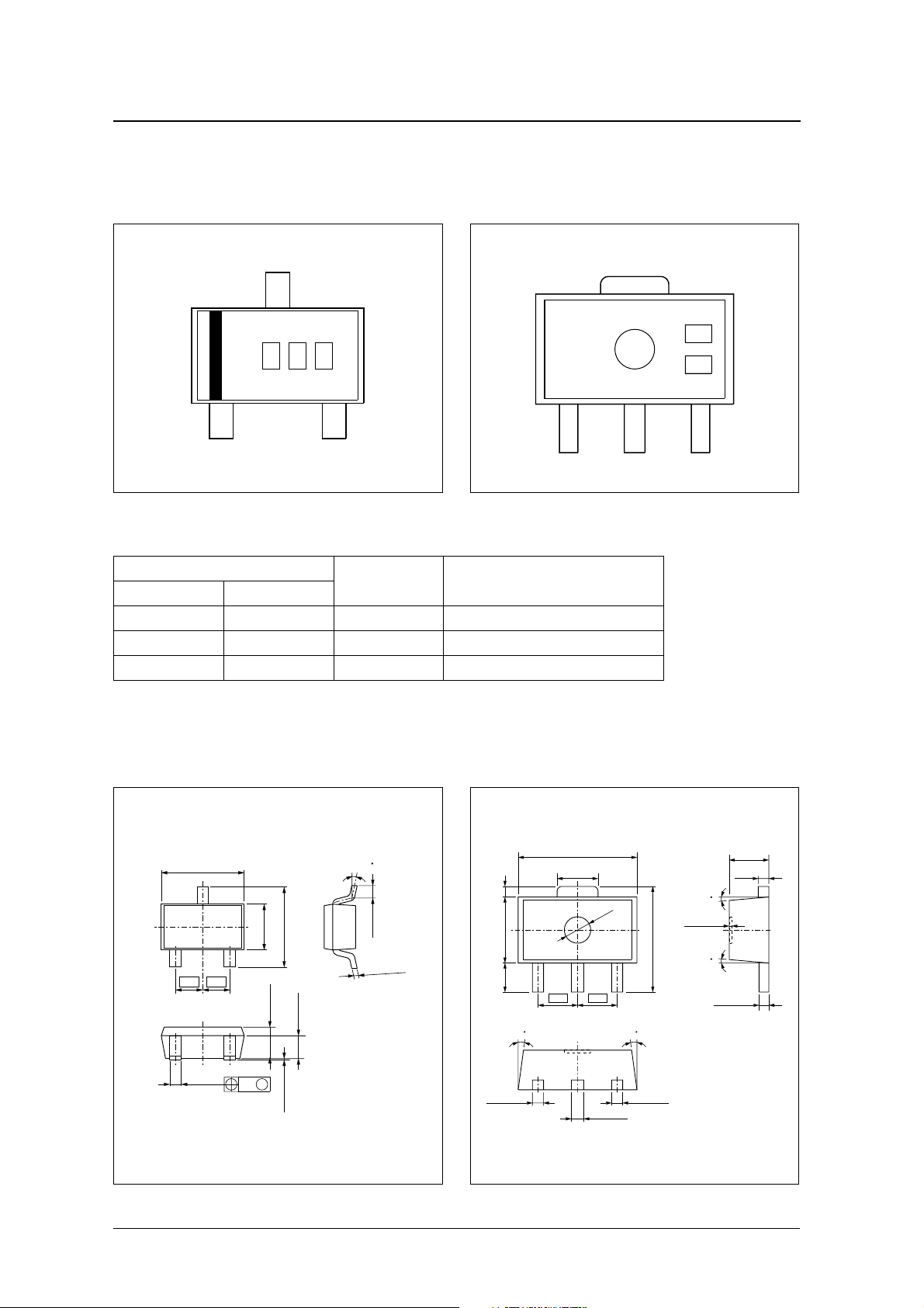
PINOUT
(Top view)
SM6702 −×× HA(SOT23 − 3) SM6702 −×× HB(SOT89 − 3)
3
20
2
12
1 23
PIN DESCRIPTION
Number
−××
SM6702
HA SM6702
1 1 VS S Ground
2 3 LX Switching pin
3 2 O UT Outpu t (device supply pin)
−××
Name Description
PACKAGE DIMENSIONS
(Unit : mm)
SM6702 −×× HA(SOT23 − 3) SM6702 −×× HB(SOT89 − 3)
2.9 ± 0.2
0 to 15
4.5 ± 0.1
1.55 ± 0.15
1.5 ± 0.1
0.4 ± 0.1
0.95 0.95
0.4 ± 0.1
0.2
1.0
φ
1.6 ± 0.2
2.8 ± 0.2
1.1 ± 0.2
0.8 ± 0.1
M
0.05 ± 0.05
0.2min
0.15
4.0 ± 0.3
0.1
±
1.1 ± 0.2 2.5 ± 0.1 (0.4)
0.42 ± 0.1 0.42 ± 0.1
(8 )
1.5 1.5
(8 )
0.47 ± 0.1
NIPPON PRECISION CIRCUITS—2
(5 )
0.1 ± 0.05
(5 )
0.37 ± 0.1
Page 3
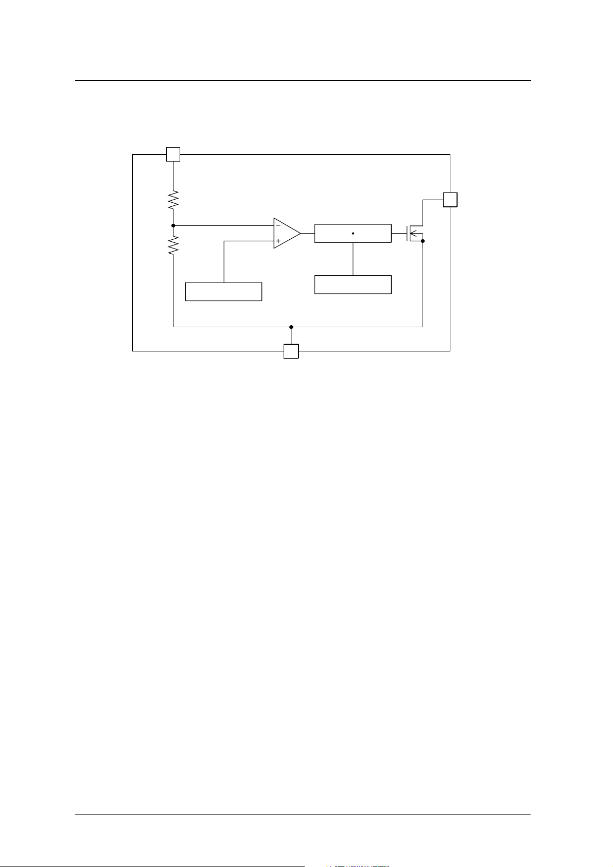
BLOCK DIAGRAM
OUT
SM6702 series
LX
PFM OSC
VREF
START−UP
VSS
NIPPON PRECISION CIRCUITS—3
Page 4

SPECIFICATIONS
Absolute Maximum Ratings
T
= 25 ° C
a
Parameter Sym bol Condition Rating Unit
LX impressed voltage V
OUT impressed voltage V
LX output current I
Po w er dissipation P
Ope rating temperature T
Storage temperature T
LX
OUT
LX
D
opr
stg
SM6702
SM6702
C
SM6702 series
−××
HA 150
−××
HB 500
5V
4V
200 mA
mW
−
20 to 70
−
40 to 125
°
C
°
Electrical Characteristics
L = 330 µH, C = 22 µF, T
Parameter Sym bol Condition
Star t-up voltage V
Holding voltage V
Current consumption I
Output voltage V
LX output current I
LX leakage current I
Maximum oscillator frequency f
Switch ON duty cycle Duty V
Input voltage range V
V
: Setting output voltage
target
= 25 ° C, V
a
st
hold
SS
OUT
LX
LXL
OSC
IN
SS
R
= 30 k
L
R
= 3 k
L
V
= 1.5 V, R
IN
V
= 1.5 V, R
IN
V
OUT
V
= 0.4 V
LX
V
OUT
V
OUT
OUT
= 0 V
Rating
min typ max
Ω
Ω
= 30 k
Ω
L
= 3 k
Ω
L
2.2
≤
V
≤
2.7 60 – –
2.8
target
≤
V
≤
3.3 80 – –
target
= V
−
0.1,
target
= V
= 3.5 V – – 1 µ A
LX
= V
−
0.1 80 100 120 kHz
target
= V
−
0.1 65 75 85 %
target
– – 0.9 V
– – 0.7 V
–816µA
V
×
target
0.975
V
target
––
V
1.025
V
target
target
0.2
Unit
×
V
mA
+
V
NIPPON PRECISION CIRCUITS—4
Page 5

SM6702 series
FUNCTIONAL DESCRIPTION
Step-up Principle
The SM6702 series use a transistor to switch the input supply in a non-isolated chopper switching regulator
configuration. The figure below shows the basic step-up switching regulator circuit.
If the transistor is ON for an interval t
the interval t
that the peak voltage reaches V
generates a voltage V
ON
IN
+ V
and then instantly turned OFF, the energy stored in the coil L during
ON
across the coil. This voltage is superimposed on the input voltage such
L
which forces the diode D to conduct and release the stored energy into
L
the output.
During normal operation, the above switching occurs repeatedly at a frequency controlled by an oscillator
(which can change depending on the input and output load conditions), generating a square wave output which
is then smoothed by the output capacitor C. Thus the output voltage (V
L
IN VOUT
V
GND
D
Tr
> V
OUT
C
) has been stepped up.
IN
PFM Control
In SM6702 series, the LX transistor ON interval is fixed, and the OFF interval varies in response to the input
voltage and load changes. Thus the resulting switching cycle frequency varies, called pulse frequency modulation.
NIPPON PRECISION CIRCUITS—5
Page 6

BASIC CIRCUIT
SM6702 series
IN OUT
V
Coil (L) : 330 µH
Diode (D) : MA721 (Matsushita Schottky diode)
Capacitor (C
L
TYPICAL APPLICATION CIRCUIT
L
L
D
OUTLX
VSS
) : 22 µF tantalum
+
C
D
3V System
Voltage
1.5V
LX
OUT
++
C1 C2 C3
VSS
Coil (L) : 330 µH
Schottky Diode (D)
Capacitor (C1) : 22 µF tantalum
Capacitor (C2) : 0.22 µF ceramic
Capacitor (C3) : 22 µF tantalum
NIPPON PRECISION CIRCUITS—6
Page 7

SM6702 series
BASIC CHARACTERISTICS SM6702-30HA (V
Output voltage vs. Output current
3.5
3
Vin=0.9V
2.5
2
1.5
1
Output Voltage Vout[V]
0.5
0
0 5 10 15 20 25 30
L=330µH, C=22µF
Output Current I
out[mA]
Efficiency vs. Output current
100
95
90
85
80
Vin=0.9V
75
70
Efficiency [%]
65
60
55
50
0 5 10 15 20 25 30
L=330µH, C=22µF
Output Current I
out
Vin=1.5V
Vin=1.2V
Vin=1.5V
Vin=1.2V
[mA]
3.5
2.5
1.5
Output Voltage Vout[V]
0.5
100
95
90
85
80
75
70
Efficiency [%]
65
60
55
50
: 3.0V)
out
L=470µH, C=22µF
out
Vin=1.5V
Vin=1.5V
[mA]
3
Vin=0.9V
2
1
0
0 5 10 15 20 25 30
Vin=0.9V
0 5 10 15 20 25 30
Output Current I
L=470µH, C=22µF
Output Current I
Vin=1.2V
out[mA]
Vin=1.2V
Ripple voltage vs. Output current
200
175
150
125
100
75
50
Ripple Voltage Vr[mVpp]
25
0
0 102030405060
L=330µH, C=22µF
Vin=1.2V
Vin=0.9V
Output Current I
Vin=1.5V
out[mA]
NIPPON PRECISION CIRCUITS—7
Page 8

SM6702 series
Output voltage vs. Temperature
3.2
3.1
3.0
Output Voltage Vout[V]
2.9
2.8
-40-200 20406080
Vin=1.5V, L=330µH, RL=3kΩ
Temperature [°C]
Start-up voltage vs. Temperature
1.0
0.8
L=330µH, RL=30kΩ
Maximum oscillator frequency vs.
Temperature
200
175
150
125
100
75
50
25
Maximum Oscillator Frequency fosc[kHz]
0
-40-200 20406080
Vout=2.9V
Temperature [°C]
Hold-on voltage vs. Temperature
1.0
0.8
L=330µH, RL=3kΩ
0.6
0.4
Start-up Voltage Vst[V]
0.2
0.0
-40-20 0 20406080
Temperature [°C]
Current consumption vs. Temperature
10
8
6
4
Current Consumption Iss[µA]
2
0
-40-200 20406080
Vin=1.5V, L=330µH, RL=30kΩ
Temperature [°C]
0.6
0.4
Hold-on Voltage Vhold[V]
0.2
0.0
-40-200 20406080
Temperature [°C]
Oscillator duty cycle vs. Temperature
90
85
80
75
70
65
Oscillator Duty Cycle [%]
60
55
50
-40 -20 0 20 40 60 80
Vout=2.9V
Temperature [°C]
NIPPON PRECISION CIRCUITS—8
Page 9

SM6702 series
LX switching current vs. Temperature LX leakage current vs. Temperature
200
175
150
125
100
75
50
LX Switching Current ILX[mA]
25
0
-40-200 20406080
Vout=2.9V
Temperature [°C]
100
10
1
LX Leakage Current ILXL[nA]
0.1
-40-200 20406080
Vin=Vout=3.5V
Temperature [°C]
NIPPON PRECISION CIRCUITS—9
Page 10

SM6702 series
NIPPON PRECISION CIRCUITS INC. reserves the right to make changes to the products described in this data sheet in order to
improve the design or performance and to supply the best possible products. Nippon Precision Circuits Inc. assumes no responsibility for
the use of any circuits shown in this data sheet, conveys no license under any patent or other rights, and makes no claim that the circuits
are free from patent infringement. Applications for any devices shown in this data sheet are for illustration only and Nippon Precision
Circuits Inc. makes no claim or warranty that such applications will be suitable for the use specified without further testing or modification.
The products described in this data sheet are not intended to use for the apparatus which influence human lives due to the failure or
malfunction of the products. Customers are requested to comply with applicable laws and regulations in effect now and hereinafter,
including compliance with export controls on the distribution or dissemination of the products. Customers shall not export, directly or
indirectly, any products without first obtaining required licenses and approvals from appropriate government agencies.
NIPPON PRECISION CIRCUITS INC.
4-3, Fukuzumi 2-chome
Koto-ku, Tokyo 135-8430, Japan
Telephone: +81-3-3642-6661
NIPPON PRECISION CIRCUITS INC.
Facsimile: +81-3-3642-6698
http://www.npc.co.jp/
Email: sales
@ npc.co.jp
NIPPON PRECISION CIRCUITS—10
NC9721CE 2000.10
 Loading...