

Page 1
≥
°
°
° C]
SM6610 series
NIPPON PRECISION CIRCUITS INC.
CMOS Monolithic Temperature Sensor IC
OVERVIEW
SM6610 series is high-accuracy temperature sensor IC in the ultra small package.
By using CMOS circuit, it realizes low voltage and low current consumption.
The power down function contributes to decrease the current consumption of application set by activating
intermittent function easily.
FEATURES
■
High linearity: ± 0.5% typ. (Ta = –20 to 80 ° C)
■
Operating temperature range: –40 to 100 ° C (V
2.7V)
■
Maximum output current load: ± 250 µ A
■
Output reference: VSS
■
Low current consumption: 5.5 µ A typ. (Ta = 25 ° C)
DD
■
Low stand-by current: 0.5 µ A max.
■
Very small plastic package: SC82AB
■
Very small leadless package: VSP-4
■
Power down function
■
Molybdenum-gate CMOS Process
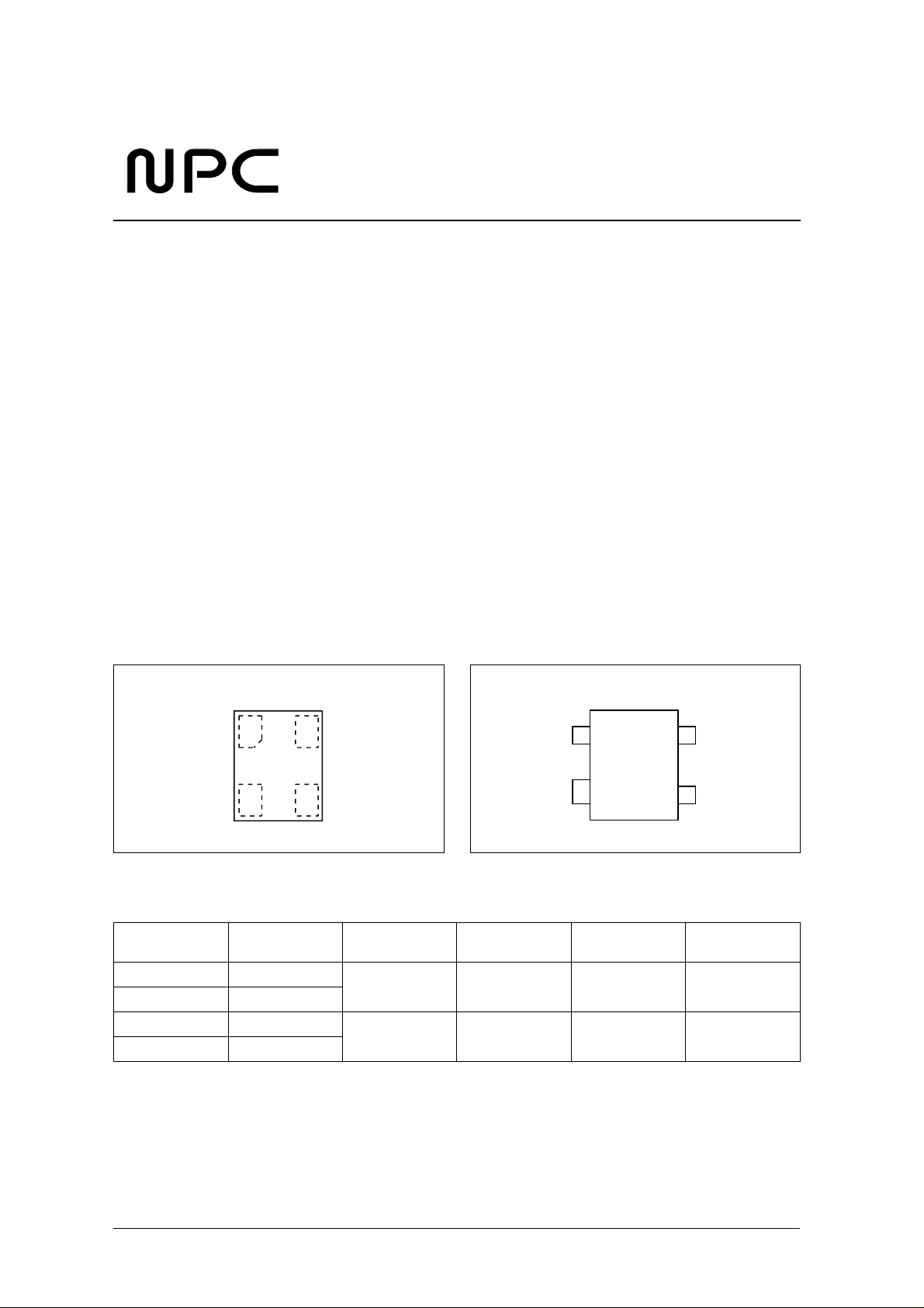
PINOUT
(Top view)
VSP-4 SC82AB
1VDD
2VSS 3 PDN
4 OUT
ORDERING INFORMATION
De vice Pack ag e
SM6610AH SC82AB
SM6610AD VSP-4
SM6610BH SC82AB
SM6610BD VSP-4
preliminary
1
VDD
2
VSS
Output center current
[V] (Ta = 25
C)
1.933 – 10.7 4.0 to 6.0 ± 5.0
1.449 – 8.2 2.4 to 6.0 ± 5.0
Temperature
coefficient [mV/
Operating voltage
C]
[V]
4
3
OUT
PDN
Accuracy
[
NIPPON PRECISION CIRCUITS—1
Page 2
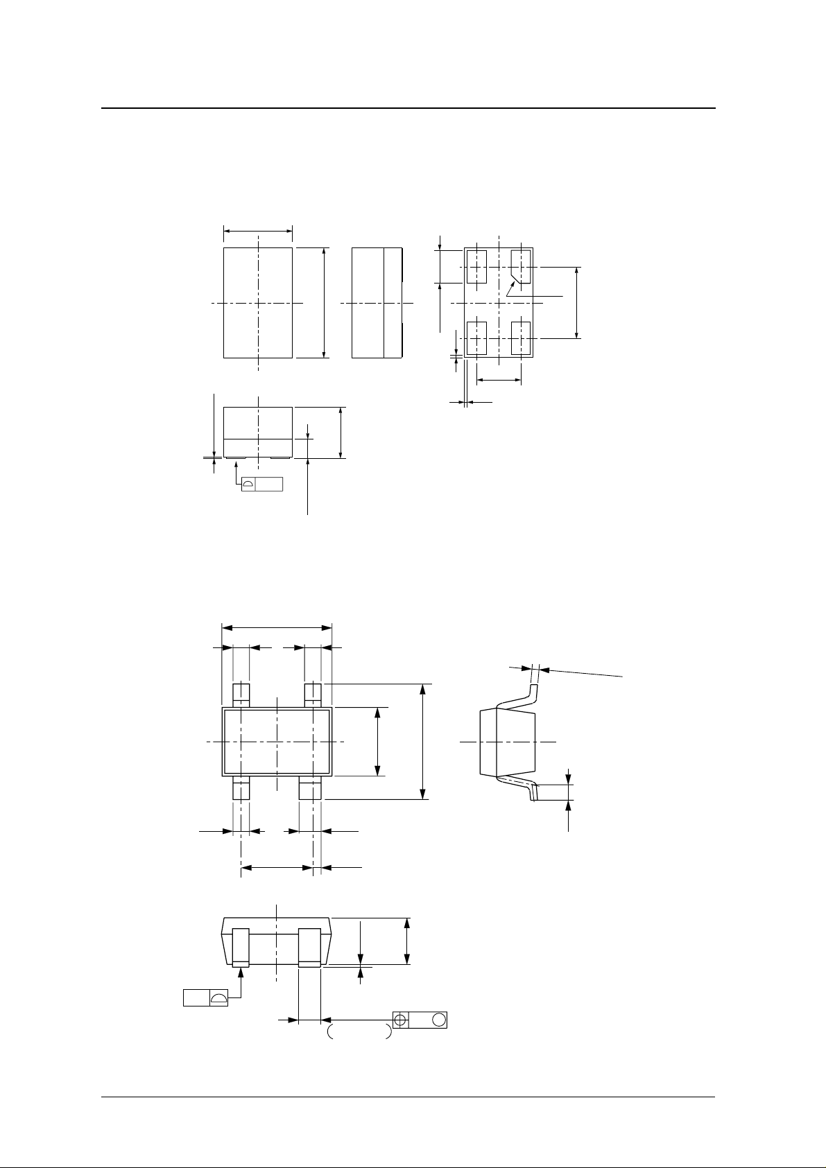
PACKAGE DIMENSIONS
(Unit : mm)
VSP-4
1.25 ± 0.1
2.0 ± 0.1
SM6610 series
C0.15
1.30
0.60 ± 0.1
0.05
0.8
0.05
SC82AB
0.02 ± 0.005
0.3
0.3
2.0
0.05
+ 0.2
− 0.1
0.33 ± 0.05
0.3
−0.1
+0.07
0.93
0.4
− 0.1
+ 0.2
1.25
2.1 ± 0.3
0.125
0.3
+ 0.1
− 0.05
1.3 ± 0.2
0.15
0 to 0.1
0.9 ± 0.1
preliminary
0.1
0.4
0.3
+ 0.1
− 0.05
+ 0.1
− 0.05
0.10 M
NIPPON PRECISION CIRCUITS—2
Page 3

BLOCK DIAGRAM
SM6610 series
VDD
Constant
current
source
−
Temperature sensor
VSS
PIN DESCRIPTION
Number Name Description
1 V D D Positive power supply
2 VS S Ground
3 PDN
4 OU T Sensor output
1. Connect PDN to VDD when the power down function is not used.
1
Power down control. Pow er dow n when LOW.
Amplifier
+
OUT
PDN
preliminary
NIPPON PRECISION CIRCUITS—3
Page 4

SPECIFICATIONS
=
=
=
−
+
DC Characteristics
V
= 5.0 V, V
DD
= 0 V, Ta = –40 to 100 ° C unless otherwise noted.
SS
µ
= −
°
×
= +
°
= +
°
= −
°
×
= +
°
= +
°
°
−
−
°
= −
+
°
×
−
°
×
−
°
×
°
°
°
°
= −
+
°
±
±
µ
±
µ
µ
SM6610 series
Parameter Symbol Condition
Current consumption I
3
1
= (a/b)
L
1, 2
100
V
(V
C
OUT
Output voltage
Temperature coefficient
Linearity
Maximum capacitive load C
Maximum output current load I
Start up time t
PDN Input voltage
1. Provisional value
2. Temperature coefficient: T
3. Linearity: N
a: Maximum d eviation between measured and approximate value in the range of – 20
b: Measured value difference between the values at – 20
No load – 5.5 10.0
DD
Ta
30
C
A
version
B
version
A
version –
B
version –
C.
OUT
T
C
N
L
L
L
D
V
IH
V
IL
(@100
Ta
25
C 1.880 1.933 1.986 V
Ta
100
C 1.077 1.130 1.183 V
Ta
30
C
Ta
25
C 1.408 1.449 1.490 V
Ta
100
C 0.793 0.834 0.875 V
Ta
30 to
100
C
Ta
20 to
80
C–
V
2.4V – –
DD
V
4.5V – –
DD
C)
V
(@
30
OUT
C))/130
C and + 80
Rating
min typ max
2.468 2.521 2.574 V
1.859 1.900 1.941 V
10.7 – mV /
8.2 – m V /
0.5 – %
– – 100 pF
– – 300
V
0.3 – – V
DD
––V
C to + 80
C.
50
250
0.3 V
SS
Unit
A
C
C
A
A
s
VTEMP(V)
a
b
−20 C 80 C
V (−20 C)
Approximate value
0 C
a
Measured value
a
V (80 C)
Ta
preliminary
NIPPON PRECISION CIRCUITS—4
Page 5

SM6610 series
TYPCAL PERFORMANCE CHARACTERISTICS (Reference value)
SM6610A ×
3.00
2.50
2.00
1.50
VOUT [V]
1.00
0.50
0.00
-60 -40 -20 0 20 40 60 80 100 120
Figure 1. Temperature vs. Output voltage
1.920
1.915
1.910
1.905
VOUT [V]
1.900
1.895
1.890
-500 0 500 1000 1500
Ta [°C]
I
Load [µA]
SM6610B ×
3.00
2.50
2.00
1.50
VOUT [V]
1.00
0.50
0.00
-60 -40 -20 0 20 40 60 80 100 120
Figure 4. Temperature vs. Output voltage
1.450
1.445
1.440
1.435
VOUT [V]
1.430
1.425
1.420
-500 0 500 1000 1500
Ta [°C]
I
Load [µA]
Figure 2. Load current vs. Output voltage
GND
GND
PDN
OUT
V
(Ta = 25 ° C, V
= 4.0V)
DD
preliminary
Figure 3. PDN start up response
(Ta = 25 ° C, V
= 4.0V, C
DD
= 100pF)
L
50µs
2.0V
1.0V
Figure 5. Load current vs. Output voltage
GND
GND
PDN
OUT
V
(Ta = 25 ° C, V
= 2.4V)
DD
Figure 6. PDN start up response
(Ta = 25 ° C, V
= 2.4V, C
DD
NIPPON PRECISION CIRCUITS—5
= 100pF)
L
2.0V
1.0V
50µs
Page 6

SM6610 series
preliminary
NIPPON PRECISION CIRCUITS INC. reserves the right to make changes to the products described in this data sheet in order to
improve the design or performance and to supply the best possible products. Nippon Precision Circuits Inc. assumes no responsibility for
the use of any circuits shown in this data sheet, conveys no license under any patent or other rights, and makes no claim that the circuits
are free from patent infringement. Applications for any devices shown in this data sheet are for illustration only and Nippon Precision
Circuits Inc. makes no claim or warranty that such applications will be suitable for the use specified without further testing or modification.
The products described in this data sheet are not intended to use for the apparatus which influence human lives due to the failure or
malfunction of the products. Customers are requested to comply with applicable laws and regulations in effect now and hereinafter,
including compliance with export controls on the distribution or dissemination of the products. Customers shall not export, directly or
indirectly, any products without first obtaining required licenses and approvals from appropriate government agencies.
NIPPON PRECISION CIRCUITS INC.
4-3, Fukuzumi 2-chome
Koto-ku, Tokyo 135-8430, Japan
NIPPON PRECISION CIRCUITS INC.
Telephone: 03-3642-6661
Facsimile: 03-3642-6698
NP9919BE 2000.02
NIPPON PRECISION CIRCUITS—6
 Loading...