

Page 1
preliminary
±
SM6503A
NIPPON PRECISION CIRCUITS INC.
Diode Array for ESD Protection
OVERVIEW
The SM6503A is the Diode array for ESD protection. 5 circuits consisted of diode element are integrated into
ultra-small 6 pin plastic package. It is the most appropriate to protect the external interface circuit of portable
equipment which requires miniaturization from ESD.
FEATURES
■
8kV ESD immunity level (IEC61000-4-2 con-
tact discharge)
■
Clamp voltage: 7.5V typ.
■
Low capacitance: 10pF typ.
■
5 circuits integrated into one package
■
Ultra-small package
• SM6503AD: 6-pin SON
• SM6503AH: SOT23-6
APPICATIONS
■
Cellular phone
■
PDA
■
Set Top Box
■
Digital Still Camera
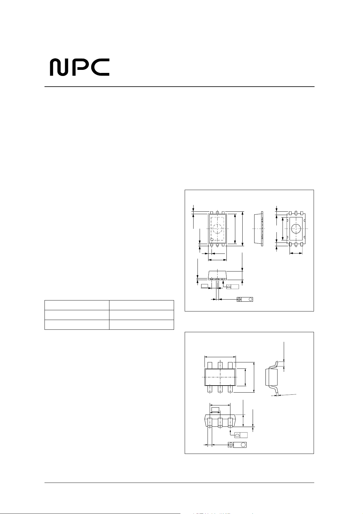
PACKAGE DIMENSIONS
(Unit: mm)
SM6503AD (6-pin SON)
0.2 ± 0.1
0.2 ± 0.1
0.3 typ.
1.6
0.125 ± 0.05
2.6 ± 0.1
+ 0.1
3.0 ± 0.1
0.75 − 0.05
(0.3)
2.0
(0.3)
1.1
ORDERING INFORMATION
Device Package
SM6503AD 6-pin SON
SM6503AH SOT23-6
0.5
+ 0.1
0.2 − 0.05
0.05
0.05
SM6503AH (SOT23-6)
2.9 ± 0.2
− 0.1
+ 0.2
1.6
1.9 ± 0.2
0.95
0.4 ± 0.1
0.12
1.1 ± 0.1
0.1
M
M
− 0.3
+ 0.2
2.8
0 to 0.15
0.15
0.45 ± 0.15
0.1
+
0.05
−
NIPPON PRECISION CIRCUITS—1
Page 2
preliminary
−
° C
µ
SM6503A
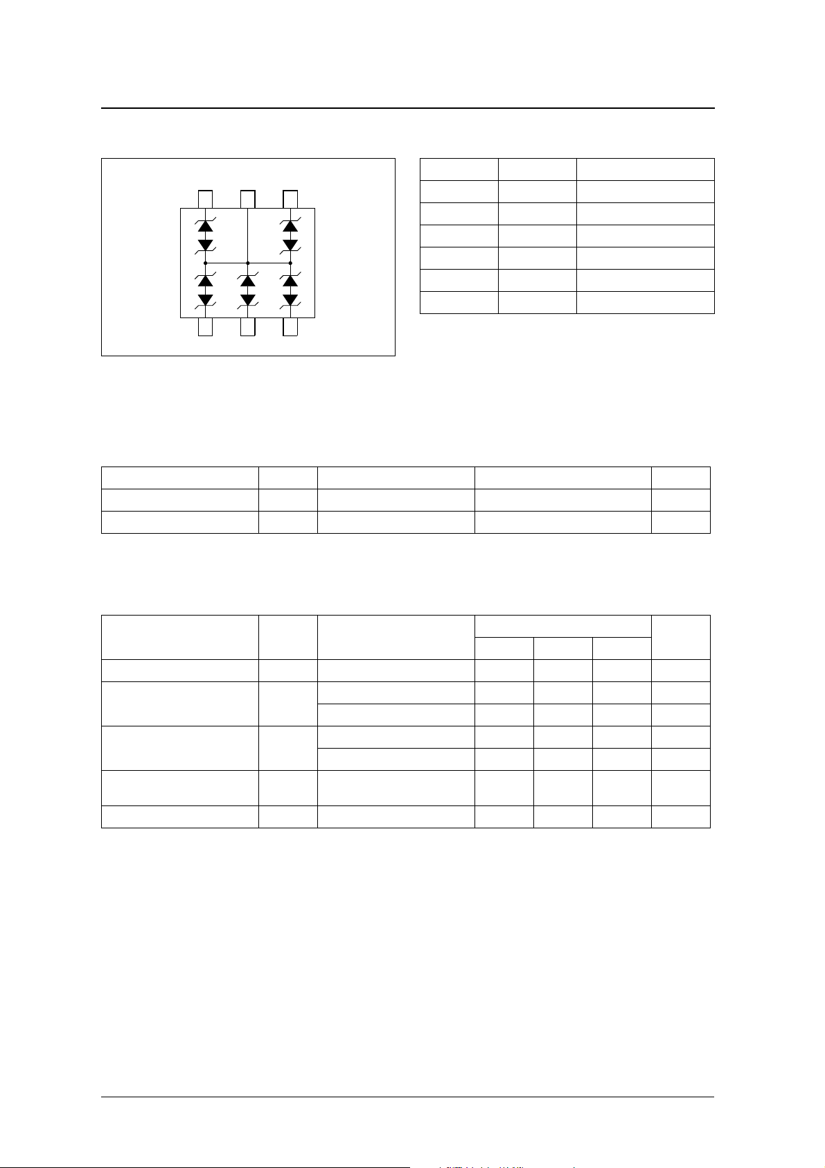
PINOUT
(Top view)
6 5 4
1 2 3
SPECIFICATIONS
Absolute Maximum Ratings
Ta = 25 ° C
Parameter Symbol Condition Rating Unit
Power dissipation P
Storage temperature range T
D
stg
PIN DESCRIPTION
Number Name Description
1 DIO1 Diode 1
2 DIO2 Diode 2
3 DIO3 Diode 3
4 DIO4 Diode 4
5 VSS Ground
6 DIO5 Diode 5
220 mW
55 to 125
Electrical Characteristics
Ta = 25 ° C
Parameter Symbol Condition
Diode maximum leakage current I
Forward clamp voltage V
Reverse clamp voltage V
Terminal capacitance C
Maximum operating voltage V
LEAK
ZF
ZR
MAX
Rating
min typ max
6V applied – – 1
I
= 1 µ A 6.5 7.5 8.5 V
Z
I
= 5mA – 6.5 – V
Z
I
= – 1 µ A – 8.5 – 7.5 – 6.5 V
Z
I
= – 5mA – – 8.0 – V
Z
f = 1MHz, between DIO1 to DIO5
T
and VSS
–10–pF
––6V
Unit
A
NIPPON PRECISION CIRCUITS—2
Page 3

preliminary
SM6503A
NIPPON PRECISION CIRCUITS INC. reserves the right to make changes to the products described in this data sheet in order to
improve the design or performance and to supply the best possible products. Nippon Precision Circuits Inc. assumes no responsibility for
the use of any circuits shown in this data sheet, conveys no license under any patent or other rights, and makes no claim that the circuits
are free from patent infringement. Applications for any devices shown in this data sheet are for illustration only and Nippon Precision
Circuits Inc. makes no claim or warranty that such applications will be suitable for the use specified without further testing or modification.
The products described in this data sheet are not intended to use for the apparatus which influence human lives due to the failure or
malfunction of the products. Customers are requested to comply with applicable laws and regulations in effect now and hereinafter,
including compliance with export controls on the distribution or dissemination of the products. Customers shall not export, directly or
indirectly, any products without first obtaining required licenses and approvals from appropriate government agencies.
NIPPON PRECISION CIRCUITS INC.
4-3, Fukuzumi 2-chome
Koto-ku, Tokyo 135-8430, Japan
Telephone: +81-3-3642-6661
NIPPON PRECISION CIRCUITS INC.
Facsimile: +81-3-3642-6698
http://www.npc.co.jp/
Email: sales
npc.co.jp
@
NP0023AE 2001.02
NIPPON PRECISION CIRCUITS—3
 Loading...