

Page 1

preliminary
SM6453AB
NIPPON PRECISION CIRCUITS INC.
3-wire Serial Data Volume Control for Headphone Amplifiers IC
OVERVIEW
The SM6453AB is a 3-wire serial data volume control for headphone amplifiers with built-in electronic volume control. Two switchable input systems are supported. It features bass boost function, auto gain control
function (AGC), power-down function, and beep input, making it ideal for use in portable electronic products.
FEATURES
■
2 stereo system inputs, 1 output system
■
12mW + 12mW output (standard, 16 Ω load, 2.0V
PINOUT
(Top view)
supply voltage)
■
Attenuation function
• 1.0dB step width
• 80-step
• + 12 to – 68dB variable range
■
Mute function
■
Low current consumption (2.3mA total, 2.4V supply voltage)
■
12dB voltage gain
■
Bass boost function (2 boost characteristics controlled by external RC network)
■
Auto gain control function (AGC)
■
Beep sound input/output circuit
■
Power-down function
■
1.9 to 3.6V operating supply voltage range
■
Silicon-gate CMOS process
MLEN
MCK
MDT
RSTN
MUTEN
PDN
BEEPI
VREF1
VREF2
1
2
3
4
5
6
7
8
9
10
DVDD1
11
AVDD1
DVSS
DVDD2
1312
LIN2
LIN1
AGCTC
LRMXO
BSTC
2829303132 2627
RIN2
RIN1
AVSS1
BSTN
25
24
23
22
21
20
19
18
17
161514
VBIAS
BSTO
BEEPLO
LOUT
AVSS2
AVDD2
AVDD3
AVSS3
ROUT
BEEPRO
PACKAGE DIMENSIONS
ORDERING INFORMATION
(Unit: mm)
Device Package
SM6453AB 32-pin QFN
32-pin QFN
TBD
NIPPON PRECISION CIRCUITS—1
Page 2
preliminary
=
=
=
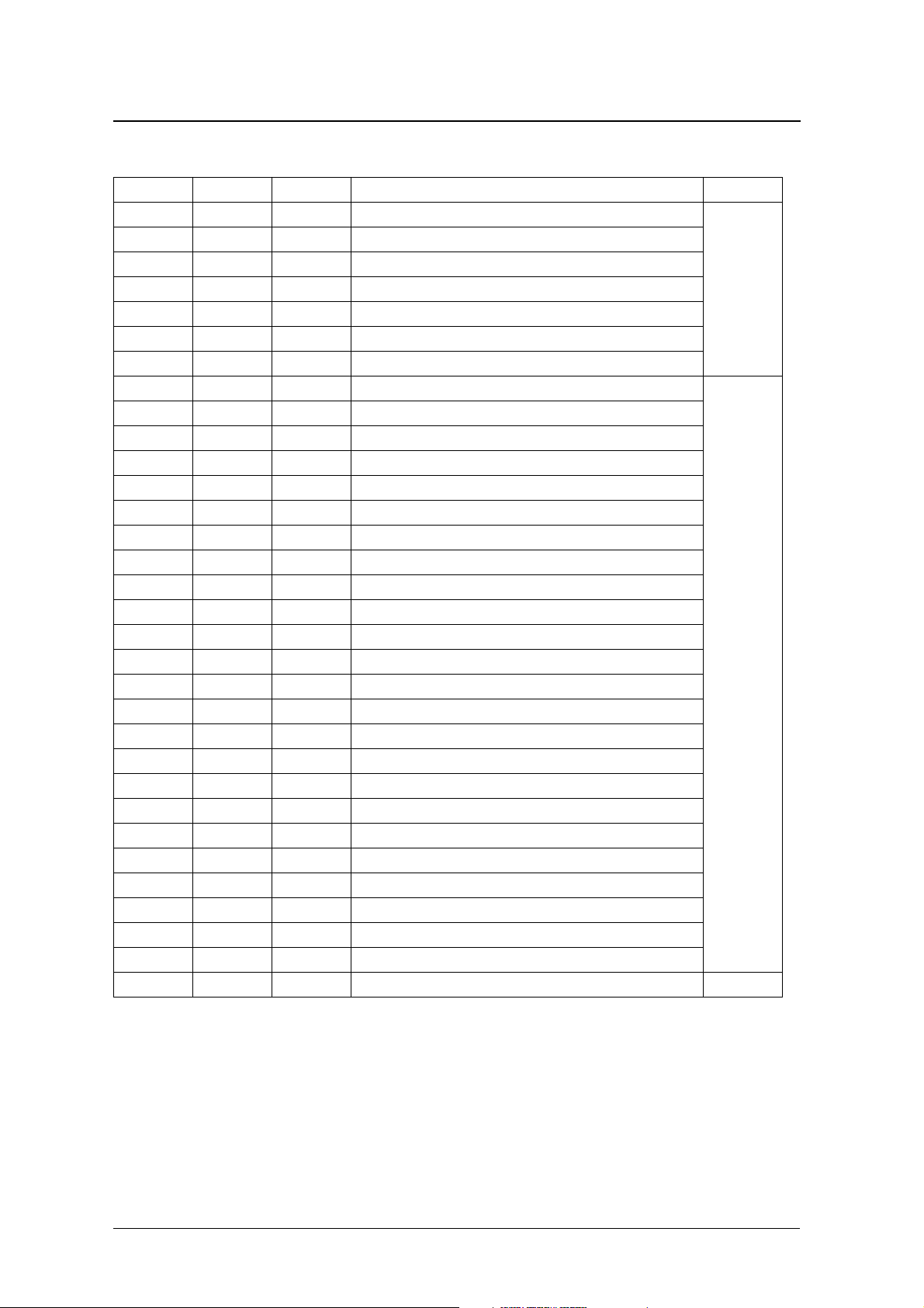
PIN DESCRIPTION
−
−
−
−
−
−
−
−
−
SM6453AB
Number Name I/O
1 MLEN Ip Microcontroller latch enable input
2 MCK Ip Microcontroller clock input
3 MDT Ip Microcontroller data input
4 RSTN Ip System reset (LOW-level reset)
5 MUTEN I Mute input (LOW-level mute)
6 PDN I Power-down mode select (LOW-level power-down)
7 BEEPI I Beep signal input
8 VREF1 O Reference voltage 1
9 VREF2 O Reference voltage 2
10 AVDD1
11 LIN1 I Left-channel analog input 1
12 LIN2 I Left-channel analog input 2
13 AVSS1
14 RIN1 I Right-channel analog input 1
15 RIN2 I Right-channel analog input 2
16 VBIAS O EVR-stage bias voltage
17 BEEPRO O Right-channel beep signal output
18 ROUT O Right-channel output
19 AVSS3
20 AVDD3
21 AVDD2
22 AVSS2
23 LOUT O Left-channel output
24 BEEPLO O Left-channel beep signal output
25 BSTO O Bass boost auxiliary output
26 BSTN I Bass boost auxiliary input
27 BSTC O Bass boost capacitor connection
28 AGCTC O AGC time constant capacitor connection
29 LRMXO O Left + right-channel mix detector output
30 DVSS
31 DVDD2
32 DVDD1
1. Ip = input with pull-up
1
EVR-stage analog V
EVR-stage analog V
Headphone amplifier right-channel analog V
Headphone amplifier right-channel analog V
Headphone amplifier left-channel analog V
Headphone amplifier left-channel analog V
Digital V
SS
Digital V
DD2
Digital V
DD1
DD
SS
Description V
SS
DD
DD
SS
DD
V
DD2
V
DD1
V
DD2
V
, V
, V
DD1
V
DD1
V
DD2
V
DVSS = AVSS1 = AVSS2 = AVSS3
SS
definition:
DD2
SS
DVDD2 = AVDD1 = AVDD2 = AVDD3
DVDD1
NIPPON PRECISION CIRCUITS—2
Page 3
preliminary
BLOCK DIAGRAM
MLEN
MCK
SM6453AB
VREF1
VDD1
+
1µF
DVDD1
DVDD231DVSS30LRMXO29AGCTC28BSTC27BSTN
32
1
2
AGC
0.1µF
22µF
26
BSTO
25
BST
BEEPLO
24
VDD2
VDD2
MDT
RSTN
MUTEN
PDN
BEEPI
VREF1
VREF2
3
4
5
6
7
8
9
AVDD1
10µF
10µF
Level Shifter
+
+
Interface
Microcontroller
40kΩ
40kΩ
EVR
EVR
VREF1
VREF2
10 11 12 13 14 15 16
LIN1
10µF
VDD1
LIN2
10µF
+
10µF
Selector
AVSS1
RIN1
220µF 16Ω
LOUT
HPA
1.6kΩ
1.6kΩ
HPA
BEEP
RIN2
10µF
10µF
+
10µF
23
22
21
20
19
18
17
VBIAS
AVSS2
AVDD2
AVDD3
AVSS3
ROUT
BEEPRO
+
0.47µF
220µF
+
+
220µF
0.47µF
+
220µF 16Ω
10Ω
VDD1
VDD1
10Ω
NIPPON PRECISION CIRCUITS—3
Page 4
preliminary
SPECIFICATIONS
Absolute Maximum Ratings
Parameter Symbol Rating Unit
V
, V
DD1
Supply voltage
Digital system input voltage V
Analog system input voltage V
Storage temperature T
Recommended Operating Conditions
V
DVSS = AVSS1 = AVSS2 = AVSS3 = 0V, V
SS
V
DD2
DVDD1
V
DD2
SS
IND
INA
STG
=
=
=
SM6453AB
0.3 to 4.6 V
0V
DVSS − 0.3 to V
AVSS − 0.3 to V
55 to 125
DD1
0.3 V
DD1
0.3 V
DD2
DVDD2 = AVDD1 = AVDD2 = AVDD3,
−
+
+
−
° C
−
°
Parameter Symbol Conditions Unit
Supply voltage 1 V
Supply voltage 2 V
Operating temperature T
Voltages between DVDD2, AVDD1, AVDD2, AVDD3 should be less ± 0.1V.
DD1
DD2
OPR
1.9 to 3.6 V
1.9 to 3.6 V
40 to 85
C
NIPPON PRECISION CIRCUITS—4
Page 5

preliminary
SM6453AB
DC Characteristics
AVSS1 = AVSS2 = AVSS3 = DVSS = 0V, AVDD1 = AVDD2 = AVDD3 = DVDD2 = 1.9 to 3.6V,
DVDD1 = 1.9 to 3.6V
µ
µ
µ
µ
µ
=
µ
Parameter Pins Symbol Condition
I
DVDD1
DVDD2
AVDD1
Current consumption
AVDD2
AVDD3
Input voltage 1 (*1)
Input voltage 2 (*2)
Input voltage 3 (*3)
Input current 1 (*1) I
Input current 2 (*3) I
Input leakage current 1 (*1) I
Input leakage current 2 (*2) I
Input leakage current 3 (*2) I
Input leakage current 4 (*3) I
DDD1A
I
DDD1S
I
DDD2A
I
DDD2S
I
DDA1A
I
DDA1S
I
DDA2A
I
DDA2S
I
DDA2T
I
DDA3A
I
DDA3S
I
DDA3T
H-level V
L-level V
H-level V
L-level V
H-level V
L-level V
IL1
IH1
IH2
IL2
IH3
IL3
IH1
IL1
IH2
IL2
IH3
IL3
Rating
min typ max
(Note 1) 0.01 0.02 mA
(Note 2) 0.2 1.0
(Note 1) 0.30 TBD mA
(Note 2) 0.2 1.0
(Note 1) 0.84 1.26 mA
(Note 2) TBD 25.0
(Note 1) 0.68 1.02 mA
(Note 2) TBD 25.0
(Note 3) TBD
(Note 1) 0.68 1.02 mA
(Note 2) TBD 25.0
(Note 3) TBD
0.7 × DVDD1 V
0.3 × DVDD1 V
1.0 V
0.4 V
1.5 V
1.0 V
V
0V 70 150
IN
V
= V
IN
DD1
V
= V
IN
DD1
V
= 0V 1.0 µA
IN
V
= V
IN
DD1
V
= 0V 1.0 µA
IN
280 420 µA
1.0 µA
1.0 µA
Unit
A
A
A
A
A
A
(Note 1) MUTEN = H-level, PDN = H-level, Analog input = – ∞ dBv, ATT = 0dB, Microcontroller clock frequency = 4MHz, data transfer from microcontroller
(Note 2) MUTEN = L-level, PDN = L-level, Analog input = – ∞ dBv, ATT = 0dB, data transfer from microcontroller stopped, Pins (*1) = V
(Note 3) MUTEN = H-level, PDN = H-level, reference voltage = Measurement circuit, Bass boost = OFF, AGC = OFF, Frequency = 1kHz, P
0.5mW
DD2
= 0.5mW +
O
Pin types
(*1)
(*2)
(*3)
Function Digital signal inputs (with pull-up)
Name MLEN, MDT, MCK, RSTN
Function Analog input 1
Name MUTEN, PDN
Function Analog input 2
Name BEEPI
NIPPON PRECISION CIRCUITS—5
Page 6

preliminary
SM6453AB
AC Characteristics
AVDD1 = AVDD2 = AVDD3 = DVDD1 = DVDD2 = 1.9 to 3.6V, VSS = 0V, Ta = − 40 to 85°C, unless
otherwise noted.
Serial inputs (MDT, MCK, MLEN)
Parameter Symbol
MCK, MLEN rise time t
MCK, MLEN fall time t
MDT setup time t
MDT hold time t
Setup time t
MLEN
MDT
MCK
Hold time t
LOW-level pulsewidth t
HIGH-level pulsewidth t
t
MDS
t
MDH
t
MCS
r
f
MDS
MDH
MCS
MCH
MEWL
MEWH
Rating
min typ max
100 ns
100 ns
50 ns
50 ns
50 ns
50 ns
50 ns
50 ns
t
MCH
Unit
0.5V
0.5V
DD2
DD2
MLEN
MLEN
MCK
Reset input (RSTN)
Parameter Symbol
RSTN LOW-level pulsewidth
0.9VDD2
0.1VDD2
0.5V
DD2
t
MEWL
t
f
t
RSTN
t
MEWH
t
r
0.9VDD2
0.1VDD2
Rating
min typ max
100 ns
Unit
NIPPON PRECISION CIRCUITS—6
Page 7

preliminary
SM6453AB
AC Analog Characteristics
V
= V
DD1
circuit, unless otherwise noted.
Analog input characteristics (LIN1, RIN1, LIN2, RIN2)
= 2.0V, analog input amplitude = 0.022Vrms, input frequency = 1kHz, Ta = 25°C, Measurement
DD2
Parameter Symbol Condition
Reference input amplitude V
Input resistance R
Input clipping voltage V
min typ max
AT T = 0dB 0.022 Vrms
AI
IN
AT T = 0dB 0.14 0.168 Vrms
CLP
45 51 57 kΩ
Rating
Analog output characteristics (LOUT, ROUT)
Parameter Symbol Condition
Residual noise voltage V
Total harmonic distor tion + noise THD + NPO = 0.5mW + 0.5mW 0.3 0.8 %
Maximum output voltage P
Bass boost response
AGC detection level V
Gain control range R
Step size STEP 0.8 1.0 1.8 dB
Attenuation error (1kHz to 20kHz)
Absolute attenuation (1kHz)
Mute factor (1kHz) MUTE ATT = MUTE, MUTEN = LOW − 84.0 − 90.0 dB
Channel crosstalk
Channel crosstalk
Ripple rejection PSRR Supply ripple on AVDD1, AVDD2, AVDD3 69.0 75.0 dB
1. Bass boost control bit D9 = HIGH, 55Hz, VO = – 30dBv
2. ATT = 0dB, leakage output on one channel with analog input on the other channel only.
3. Bass boost control bit D9 = HIGH, ATT = 0dB, leakage output on one channel with analog input on the other channel only.
1
2
3
B
ERR1 @ 12dB to − 48dB TBD 0.2 TBD dB
ERR2 @ − 49dB to − 68dB TBD 0.5 TBD dB
AT T = 0dB 20 30 µVrms
NS
AT T = 0dB, THD = 10% 15 20 mW
OMAX
BST
AGC
CNT
AT
AT T = 0dB + 12.0 dB
0
AT
AT T = − 20dB − 8.0 dB
2
AT
AT T = − 40dB − 28.0 dB
4
AT
AT T = − 60dB − 48.1 dB
6
AT
AT T = − 80dB − 68.2 dB
8
CT
1
CT
2
min typ max
− 68 12 dB
− 84.0 − 90.0 dB
− 24.0 − 40.0 dB
Rating
+ 13.5 dB
0.55+
0.5V
DD1
Unit
Unit
V
Analog output characteristics (BEEPLO, BEEPRO)
Parameter Symbol Condition
BEEP output current I
BEEP output voltage V
BO
400Hz rectangular wave,
input level = 1.5V to V
BO
DD2
Rating
min typ max
0.3 0.36 0.4 mA
− 56 − 51.3 − 46 dBv
NIPPON PRECISION CIRCUITS—7
Unit
Page 8

preliminary
SM6453AB
Reference voltage characteristics (VREF1, VREF2, VBIAS)
Parameter Symbol Condition
Reference voltage output 1 V
Reference voltage output 2 V
Bias voltage output V
Measurement circuit
DVDD132DVDD231DVSS
1
MLEN
2
MCK
3
MDT
4
RSTN
5
6
7
8
9
MUTEN
PDN
BEEPI
VREF1
VREF2
VDD2
VDD2
REF1
REF2
BIAS
VDD1
+
1µF
22µF
30
29
LRMXO
AGCTC28BSTC27BSTN
NPC
SM6453
Rating
min typ max
VREF1
0.45V
0.45V
0.1µF
DD1
DD1
26
BSTO
BEEPLO
LOUT
AVSS2
AVDD2
AVDD3
AVSS3
ROUT
BEEPRO
V
DD1 −
0.5V
0.5V
25
24
23
22
21
20
19
18
17
DD1
0.815 V
DD1
0.55V
0.55V
220µF 16Ω
+
0.47µF
220µF
+
+
220µF
0.47µF
+
220µF 16Ω
DD1
DD1
10Ω
VDD1
VDD1
10Ω
Unit
V
V
AVDD1 LIN1
10 11 12 13 14 15 16
+
10µF
+
10µF
VDD1
LIN2
AVSS1 RIN1 RIN2 VBIAS
10µF
+
10µF
10µF
10µF
10µF
+
10µF
NIPPON PRECISION CIRCUITS—8
Page 9

preliminary
SM6453AB
FUNCTIONAL DESCRIPTION
Microcontroller Interface
The SM6453AB uses a serial microcontroller interface comprising MDT (data), MCK (clock), MLEN (latch
enable).
Data format
The data transfer format is shown in figure 1.
D15 D14 D13 D12 D11 D10 D9 D8 D7 D6 D5 D4 D3 D2 D1 D0MDT
MCK
MLEN
Figure 1. Microcontroller data input timing
The internal shift register shifts data on the rising edge of MCK, and the data is loaded and updated on the rising edge of MLEN (the dotted lines are all valid data timing). Each cycle is completed by 16 or more MCK
input cycles, even if there are unused data bits.
NIPPON PRECISION CIRCUITS—9
Page 10

preliminary
Microcontroller data description
SM6453AB
“L” = V
■ D15 to D12: Not used (Don’t Care) bits. Can be either “L” or “H”.
■ D11: AGC bit. OFF when “L”, and ON when “H”.
■ D10, D9: Bass boost control bit.
■ D8: Input select bit. LIN1 and RIN1 when “L”, and LIN2 and RIN2 when “H”.
level, “H” = V
IL1
D11 AGC function
L OFF
HON
D9 D10
L
H
D8 Selected inputs
L LIN1, RIN1
H LIN2, RIN2
level
IH1
L
H
L BB1
H BB2
Bass boost
characteristics
OFF
■ D7 to D0: Attenuation (ATT) bits.
Amp gain EVR ATT value D7 D6 D5 D4 D3 D2 D1 D0 HEX
+ 12dB 0dB LLLLLLLL00
+ 11dB − 1dB LLLLLLLH01
+ 10dB − 2dB LLLLLLHL02
: : :::::::::
− 3dB − 15dB LLLLHHHH0F
− 4dB − 16dB L L L H LLLL10
− 5dB − 17dB L L L H L L L H 11
: : :::::::::
− 52dB − 63dB L L HHHHHH3F
− 53dB − 64dB L H LLLLLL40
− 54dB − 65dB L H LLLLLH41
: : :::::::::
− 67dB − 79dB L H L L HHHH4F
− 68dB − 80dB LHLHLLLL50
MUTE MUTE LHLHLLLH51
MUTE MUTE LHLHLLHL52
MUTE MUTE :::::::::
MUTE MUTE HHHHHHH LFE
MUTE MUTE HHHHHHHHFF
Note: At system reset, AGC = OFF, bass boost = OFF, LIN1 and RIN1 input, MUTE are selected.
NIPPON PRECISION CIRCUITS—10
Page 11

SM6453AB
preliminary
Bass Boost Function (BSTO, BSTN, BSTC)
Using the bass boost function, the left-channel and right-channel bass components are sampled and amplified,
or boosted, and added to the headphone driver amplifier. The connection of 0.1µF (std) capacitor to BSTC
forms a lowpass filter. The bass boost response can also be selected using bit D12.
Usually there is no component connected to BSTO and BSTN, however, the boost response characteristic can
be modified by connecting a resistor and capacitor between BSTO and BSTN.
NIPPON PRECISION CIRCUITS—11
Page 12

preliminary
SM6453AB
Auto-gain Control
The output level from the bass boost circuit can be controlled to prevent the output from exceeding a value
VREF1 [V] + 0.55 [Vpeak].
The output clip level margin is increased when bass boost is ON.
Mute Function (MUTEN)
Mute is ON when MUTEN = “L”. The mute setting is also controlled by microcontroller data. A pull-down
resistor can be added to prevent malfunction.
Power-down Function (PDN)
Power-down function is ON when PDN=“L”. A pull-down resistor can be added to prevent malfunction.
Beep Signal Input/Output (BEEPI, BEEPLO, BEEPRO)
The beep output circuit operates when MUTEN = “L”. The beep output is a fixed-current output on BEEPLO
and BEEPRO.
NIPPON PRECISION CIRCUITS INC. reserves the right to make changes to the products described in this data sheet in order to
improve the design or performance and to supply the best possible products. Nippon Precision Circuits Inc. assumes no responsibility for
the use of any circuits shown in this data sheet, conveys no license under any patent or other rights, and makes no claim that the circuits
are free from patent infringement. Applications for any devices shown in this data sheet are for illustration only and Nippon Precision
Circuits Inc. makes no claim or warranty that such applications will be suitable for the use specified without further testing or modification.
The products described in this data sheet are not intended to use for the apparatus which influence human lives due to the failure or
malfunction of the products. Customers are requested to comply with applicable laws and regulations in effect now and hereinafter,
including compliance with export controls on the distribution or dissemination of the products. Customers shall not export, directly or
indirectly, any products without first obtaining required licenses and approvals from appropriate government agencies.
NIPPON PRECISION CIRCUITS INC.
4-3, Fukuzumi 2-chome
Koto-ku, Tokyo 135-8430, Japan
Telephone: +81-3-3642-6661
NIPPON PRECISION CIRCUITS INC.
Facsimile: +81-3-3642-6698
http://www.npc.co.jp/
Email: sales
@npc.co.jp
NIPPON PRECISION CIRCUITS—12
NP0024AE 2001.02
 Loading...