

Page 1
SM6452AM/BM
NIPPON PRECISION CIRCUITS INC.
Audio Variable V olume ICs
OVERVIEW
The SM6452AM/BM are serial-control electronic variable volume ICs for audio applications. They provide
electronic volume control for 6 channels, with independent channel gain, attenuation and muting. They feature
enhanced digital zip noise suppression. The serial control options are 3-wire interface (SM6452AM) and I
bus (SM6452BM). The SM6452AM/BM are available in 24-pin SSOP packages.
FEATURES
■
6-channel input/output (positive-phase-sequence
output)
■
Attenuation function
• 6-channel independent control
• +16 to 0 to − 79dB variable range
• 1.0 dB/step adjustment
• Mute function
■
Microcontroller interface
• 3-wire serial data interface (SM6452AM)
2
•I
C bus format 2-wire control (SM6452BM)
2
•I
C address = 1000000
■
Low noise
• ≤ 0.002% THD + noise
• ≤ 10µVrms residual noise
■
0.5AV
■
Power supply
• 7 to 13V analog supply
• 2.7 to 5.5V digital supply
■
Molybdenum-gate CMOS process
■
24-pin SSOP
analog reference voltage source built-in
DD
*1
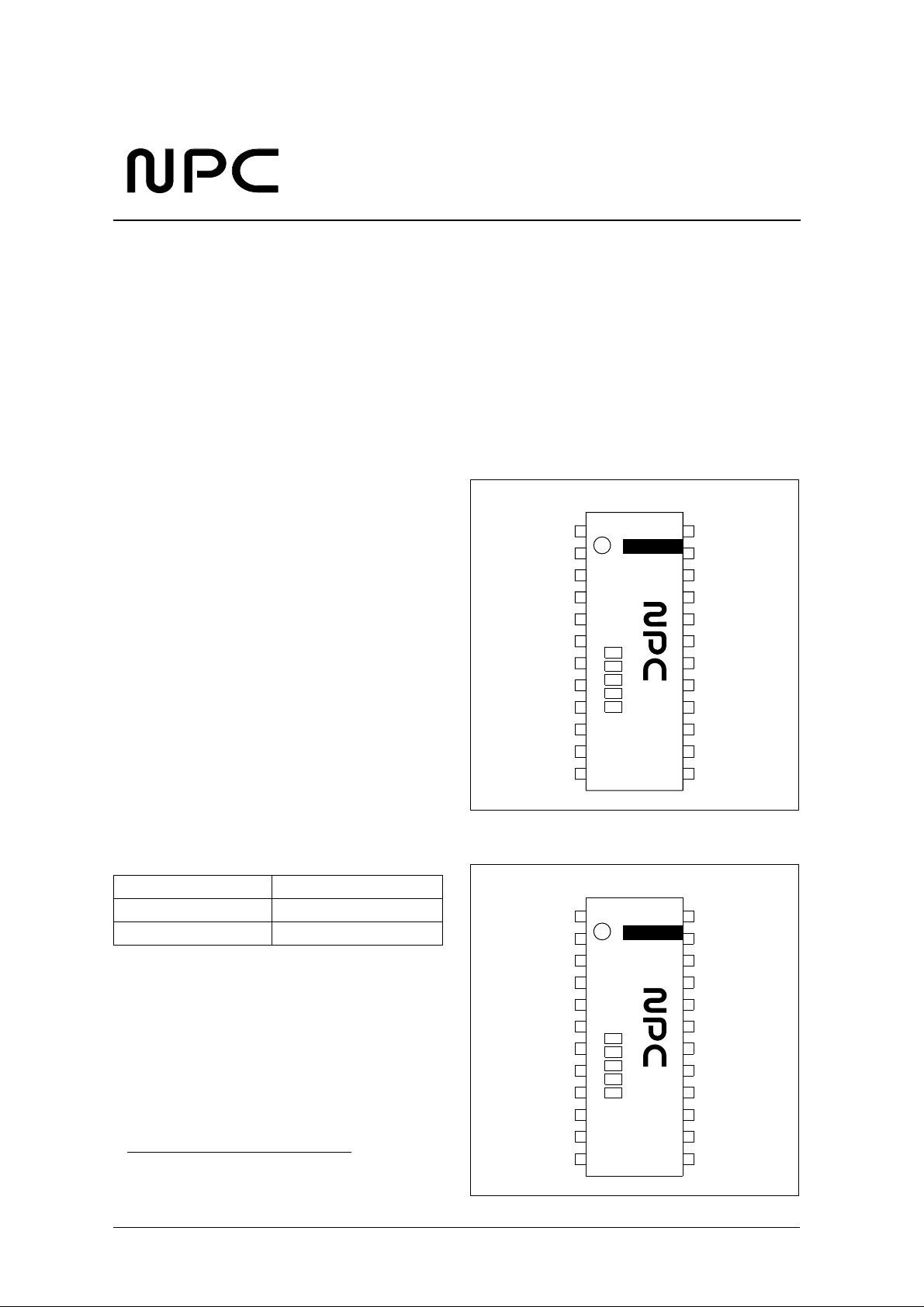
PINOUT
SM6452AM
AVDD1
VREF1
DVDD
Top view
1
AIN1
AIN2
AIN3
AIN4
AIN5
AIN6 AOUT6
AVSS1
MDT
RSTN
12
SM6
452 M
A
24
13
AVDD2
VREF2
AOUT1
AOUT2
AOUT3
AOUT4
AOUT5
AVSS2
DVSS
MCK
MLEN
2
C
ORDERING INFORMATION
De vice Pack ag e
SM6452AM 24-pin SSOP
SM6452BM 24-pin SSOP
2
*1. I
C bus is a registered trademark of Philips
Electronics N.V.
preliminary
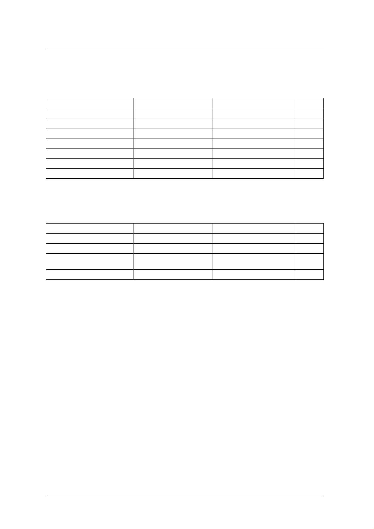
SM6452BM
AVDD1
VREF1
DVDD
Top view
1
AIN1
AIN2
AIN3
AIN4
AIN5
AIN6 AOUT6
AVSS1
SDA
RSTN
12
NIPPON PRECISION CIRCUITS—1
SM6
452 M
B
24
13
AVDD2
VREF2
AOUT1
AOUT2
AOUT3
AOUT4
AOUT5
AVSS2
DVSS
SCL
NC
Page 2

PACKAGE DIMENSIONS
Unit: mm
10.05 0.20
10.20 0.30
SM6452AM/BM
7.80 0.30
5.40 0.20
0.15
+
−
0.1
0.05
0.8
BLOCK DIAGRAM
AIN1
AIN2
AIN3
AIN4
AIN5
AIN6
0.36 0.10
0.10
AVDD1
ATT
Control
ATT
Control
ATT
Control
ATT
Control
ATT
Control
ATT
Control
0.12
M
1.80
+0.20
−0.10
1.90
0.10 0.10
Gain/ATT
Control
Gain/ATT
Control
Gain/ATT
Control
Gain/ATT
Control
Gain/ATT
Control
Gain/ATT
Control
0.50 0.20
010
AVDD2
AOUT1
AOUT2
AOUT3
AOUT4
AOUT5
AOUT6
Gain/ATT Decoder
VREF1
AVSS1
DVDD
Interface Control
MDT(AM)/SDA(BM)
RSTN
MLEN(AM)/NC(BM)
MCK(AM)/SCL(BM)
DVSS
VREF2
AVSS2
preliminary
NIPPON PRECISION CIRCUITS—2
Page 3

PIN DESCRIPTION
SM6452AM/BM
Number Name I/O
1 AVDD1 – A Analog supply 1
2 VREF1 O A Reference voltage source capacitor connection (0.5AVDD1)
3 AIN1 I A Channel 1 audio input
4 AIN2 I A Channel 2 audio input
5 AIN3 I A Channel 3 audio input
6 AIN4 I A Channel 4 audio input
7 AIN5 I A Channel 5 audio input
8 AIN6 I A Channel 6 audio input
9 AVSS1 – A Analog ground 1
10 DV DD – D Digital supply
MDT (AM) I D Microcontroller data input
11
SD A (BM) I/O D I
12 RSTN Ip D System reset input (active L OW-level)
MLEN (AM) Ip D Microcontroller latch enable input
13
NC (BM) – – No connection
MCK (AM) I D Microcontroller clock input
14
SCL (BM) I D I
15 D VS S – D Digital ground
16 AVSS2 – A Analog ground 2
17 AOUT6 O A Channel 6 audio output
18 AOUT5 O A Channel 5 audio output
19 AOUT4 O A Channel 4 audio output
20 AOUT3 O A Channel 3 audio output
21 AOUT2 O A Channel 2 audio output
22 AOUT1 O A Channel 1 audio output
23 VREF2 O A Reference voltage source capacitor connection (0.5AVDD2)
24 AVDD2 – A Analog supply 2
1. Ip = input pin with pull-up
2. A = analog, D= digital
1
A/D
2
2
C b us ser ial data input and ackn owledge (ACK) signal output
2
C bus clock input
Description
preliminary
NIPPON PRECISION CIRCUITS—3
Page 4
−
−
−
−
−
−
SPECIFICATIONS
Absolute Maximum Ratings
−
−
−
°
−
°
SM6452AM/BM
AVSS1 = AVSS2 = DVSS = 0V, AVDD1 = AVDD2 = AV
Parameter Symbol Rating
Analog supply voltage AV
Digital supply voltage DV
Analog input voltage V
Digital input voltage V
2
I
C b us signal input voltage (SDA, SCL) V
Storage temperature range T
Po w er dissipation P
1. Ratings also apply at supply switch ON and OFF.
DD
DD
INA
IND
IOPEN
stg
D
Recommended Operating Conditions
AVSS1 = AVSS2 = DVSS = 0V
Parameter Symbol Rating Unit
Analog supply voltage AV
Digital supply voltage DV
AV
Supply voltage deviation
Operating temperature T
AV
DD1
SS1
AV
DV
DD2
SS
DD
DD
, AV
, AV
opr
SS1
SS2
, DVDD = DV
DD
AV
,
SS2
DV
SS
DD
1
0.3 to 15.0 V
0.3 to 7.0 V
V
0.3 to AV
SS
V
0.3 to DV
SS
55 to 125
7.0 to 13.0 V
2.7 to 5.5 V
+ 0.3 V
DD
+ 0.3 V
DD
10 V
TBD m W
±0.1 V
40 to 85
Unit
C
C
preliminary
NIPPON PRECISION CIRCUITS—4
Page 5
DC Characteristics (SM6452AM)
AV
= 7 to 13V, DV
DD
= 2.7 to 5.5V, V
DD
SM6452AM/BM
= 0V, T
SS
= − 40 to 85 ° C
a
Parameter Symbol Condition
I
DVDD current consumption
AVDD1, AVDD2 current consumption I
MD T, MCK, MLEN, RSTN HIGH-level
input voltage
MD T, MCK, MLEN, RSTN LOW-level
input voltage
RSTN, MLEN input current I
M D T, MCK input leakage current
RSTN, MLEN input leakage current I
DDD1
I
DDD2
DDA
V
V
IL1
I
LL1
I
LH1
LH2
IH
IL
DC Characteristics (SM6452BM)
AV
= 7 to 13V, DV
DD
Parameter Symbol Condition
DVDD current consumption
AVDD1, AVDD2 current consumption I
SD A, SCL, RSTN HIGH-level input
voltage
SD A, SCL, RSTN LOW-level input
voltage
RSTN input current I
S DA, SCL input current I
RSTN input leakage current I
S DA, SCL input leakage current
S D A L OW -level output voltage V
= 2.7 to 5.5V, V
DD
I
DDD1
I
DDD2
DDA
V
V
IL1
IL2
LH1
I
LH2
I
LH3
OL
IH
IL
Rating
min typ max
Data transfer stopped, MDT = MCK =
MLEN = RSTN = DV
Data transfer in progress, DV
V
= 0V – TBD TBD µA
IN
V
= 0V – – TB D µA
IN
V
= DV
IN
DD
V
= DV
IN
DD
= 0V, T
SS
Data transfer stopped,
SD A = SCL = RSTN = DV
Data transfer in progress – TBD T B D mA
V
IN
V
IN
V
IN
V
IN
V
IN
ACK signal output, 3mA input current TB D – TBD V
= − 40 to 85 ° C
a
= 0V – TBD TBD µA
= 0V – TBD TBD µA
= DV
DD
= DV
DD
= 10V – – TB D µA
= 5V
DD
= 5V – TBD TBD mA
DD
DD
– TBD TBD µA
– TBD TBD m A
0.7DV
DD
– – 0.3DV
– – TBD µA
– – TBD µA
min typ max
– TBD TBD µA
– TBD TBD m A
0.7DV
DD
– – 0.3DV
– – TBD µA
– – TBD µA
––V
DD
Rating
––V
DD
Unit
V
Unit
V
preliminary
NIPPON PRECISION CIRCUITS—5
Page 6

SM6452AM/BM
AC Digital Characteristics (SM6452AM)
AV
= 7 to 13V, DV
DD
Serial inputs (MDT, MCK, MLEN)
= 2.7 to 5.5V, V
DD
= 0V, T
SS
= − 40 to 85 ° C
a
Parameter Symbol
MCK, MLEN rise time t
MCK, MLEN fall time t
MDT setup time t
MDT hold time t
MLEN setup time t
MLEN hold time t
MLEN LOW-level pulsewidth t
MLEN HIGH-level pulsewidth t
MDT
tMDS
MCK
tMDH
tMCS
tMEWL tMEWH
MEWL
MEWH
r
f
MDS
MDH
MCS
MCH
Rating
Unit
min typ m ax
– – 100 ns
– – 100 ns
50 – – ns
50 – – ns
50 – – ns
50 – – ns
50 – – ns
50 – – ns
0.5DVDD
0.5DVDD
tMCH
0.5DVDDMLEN
Reset input (RSTN)
Parameter Symbol
RSTN LOW-level pulsewidth t
preliminary
RSTN
Rating
Unit
min typ m ax
100 – – ns
NIPPON PRECISION CIRCUITS—6
Page 7

SM6452AM/BM
AC Digital Characteristics (SM6452BM)
AVDD = 7 to 13V, DVDD = 2.7 to 5.5V, VSS = 0V, Ta = −40 to 85°C
Serial inputs (SDA, SCL)
Parameter Symbol
SCL hold time (start) t
SCL setup time (stop) t
S DA hold time t
S DA setup time t
SCL clock HIGH-level pulsewidth t
SCL clock LOW -level pulsewidth t
SCL rise time t
SCL fall time t
SDA
tSU:DAT
SCL
HD:STA
SU:STA
HD:DAT
SU:DAT
tHIGH tLOW
HIGH
LOW
r
f
Rating
Unit
min typ m ax
4.0 – – µs
4.0 – – µs
5.0 – – µs
250 – – ns
4.0 – – µs
4.7 – – µs
– – 1000 ns
– – 300 ns
tHD:DAT tHD:STOtHD:STA
Reset input (RSTN)
Parameter Symbol
RSTN LOW-level pulsewidth t
preliminary
RSTN
Rating
Unit
min typ m ax
100 – – ns
NIPPON PRECISION CIRCUITS—7
Page 8

SM6452AM/BM
AC Analog Characteristics
AVDD = 9V, DVDD = 5V, (TBD)Vrms analog input amplitude, 1kHz analog input frequency, 100kΩ output
load resistance, Ta = 25°C, AC-coupled inputs
Analog inputs (AIN1 to AIN6)
Parameter Symbol Condition
Reference input amplitude V
Input resistance
Input clipping voltage V
1. RIN varies with the ATT setting. See figure 11 in the Analog Performance Characteristics section.
1
R
AI
IN
CLP
ATT = 0dB TBD TBD TBD Ω
THD + N = 1%, ATT = 0dB – T BD – Vrm s
min typ m ax
– TBD – Vrms
Rating
Analog outputs (AOUT1 to AOUT6)
Parameter Symbol Condition
Residual noise voltage V
Signal-to-noise ratio S NR T BD T BD – d Br
Total harmonic distortion + noise THD + N
Gain control range R
Step size Step 0.8 1.0 1.5 dB
Attenuation error (1 to 20kHz)
Absolute attenuation (1kHz)
Mute attenuation (1kHz) Mute ATT = Mute TB D TB D – dB
Channel crosstalk
Frequency response FR ATT = 0dB, f = 200kHz – T B D – dB
Quiescent output zip noise voltage
Minimum driver load resistance R
1. Leakage to other channels when analog input is applied to one channel only.
2. Noise occurring when the ATT setting is changed (peak to peak)
1
2
NS
CNT
ERR
ERR
AT
0
AT
1
AT
2
AT
3
AT
4
AT
5
CT ATT = 0dB TB D T B D – dB
N
J
ML
Input signal: 0Vrm s ,
A- w eight filter, 0dBr =
(TBD)Vrm s, ATT = 0dB
ATT = 0 dB, 20kHz lowpass
filter
+16 to −60dB TBD – TB D dB
1
−
2
61 to −79dB TBD – T BD dB
ATT = 16dB – T BD – dB
ATT = 0dB – TB D – dB
ATT = −20dB – T BD – dB
ATT = −40dB – T BD – dB
ATT = −60dB – T BD – dB
ATT = −79dB – T BD – dB
0Vr ms input signal – – T BD mVp-p
ATT = 0dB, THD + N = 1% TB D TB D – Ω
min typ m ax
– TBD TBD
– TBD TBD %
−
79 – +16 dB
Rating
Unit
Unit
µ
Vrm s
Reference voltage (VREF1, VREF2)
Parameter Symbol Condition
Reference voltage output V
preliminary
REF
Rating
min typ m ax
0.45AV
0.5AV
DD
DD
NIPPON PRECISION CIRCUITS—8
0.55AV
DD
Unit
V
Page 9

MEASUREMENT CIRCUIT
SM6452AM/BM
TBD
preliminary
NIPPON PRECISION CIRCUITS—9
Page 10
SM6452AM/BM
MICROCONTROLLER INTERFACE
SM6452AM
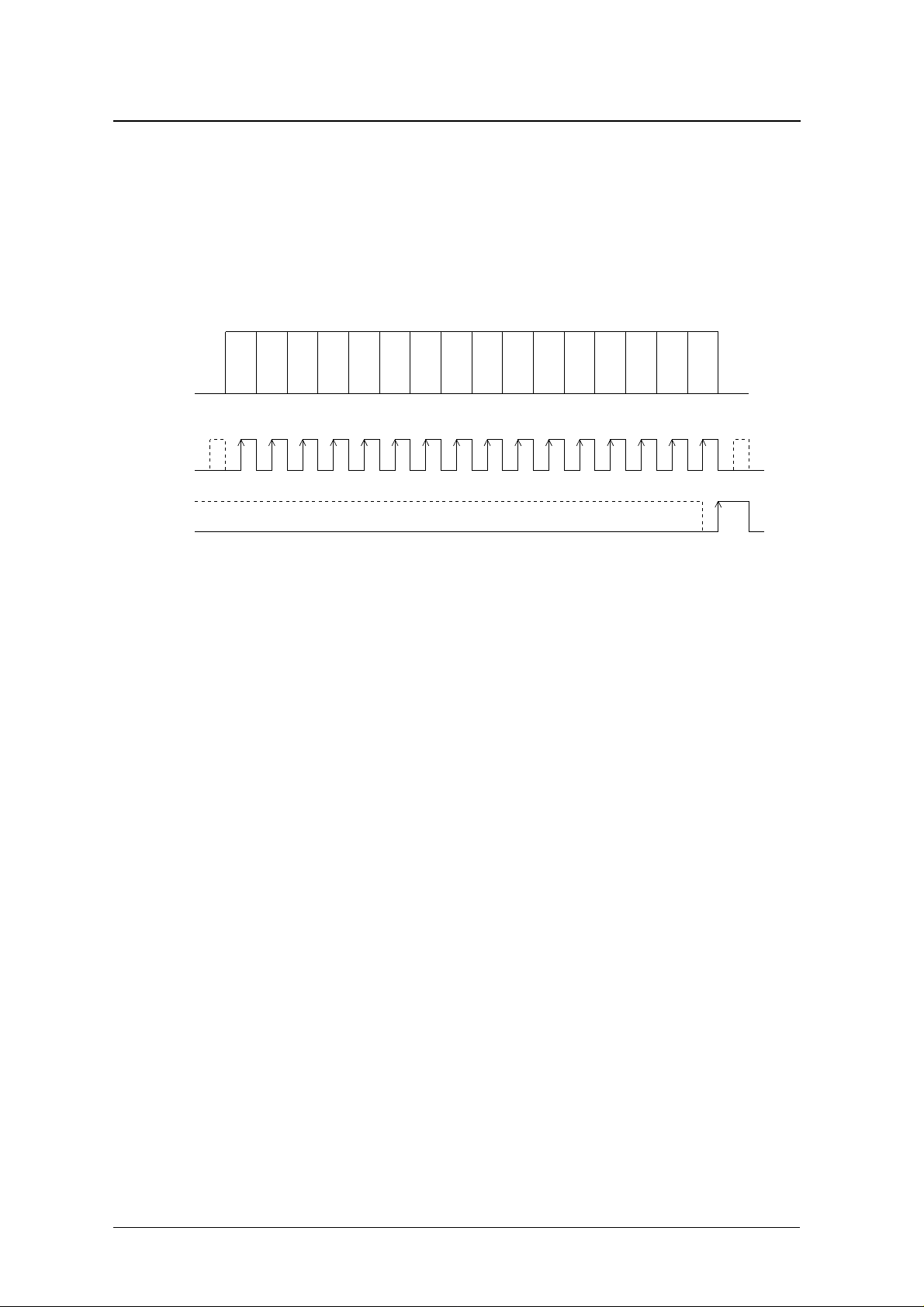
Transfer format
The SM6452AM uses a 3-wire serial interface to select channels and set attenuation levels. The transfer format
is shown in figure 1.
Care
Care
Don't
Don't
MDT
D15 D14 D13 D12 D11 D10 D9 D8 D7 D6 D5 D4 D3 D2 D1 D0
MCK
MLEN
Data is shifted into the internal shift register on the rising edge of MCK, and the attenuation value is loaded and
changed on the rising edge of MLEN. Accordingly, data on MDT should be changed on the falling edge of
MCK. The dotted lines for MCK and MLEN also indicate valid timing.
Data description (D15 to D0)
In the following description, LOW implies VIL level and HIGH implies VIH level.
■ D15, D14
Don’t care.
■ D13 to D8
Chip address bits. Each of 6 channels is set when the corresponding bit is set HIGH.
• D13: channel 1
• D12: channel 2
• D11: channel 3
• D10: channel 4
• D9: channel 5
• D8: channel 6
■ D7 to D0
Gain/attenuation set bits. The gain/attenuation setting for ATT register settings are shown in table 1.
Channel1
Channel3
Channel4
Channel 2
Figure 1. Microcontroller input data timing
Channel5
Don't
Channel6
Care
Attenuation
Data 6
Attenuation
Data 5
Attenuation
Data 4
Data 3
Attenuation
Attenuation
Data 2
Attenuation
Data 1
Data 0
Attenuation
preliminary
NIPPON PRECISION CIRCUITS—10
Page 11

SM6452AM/BM
SM6452BM
Transfer format
The SM6452BM uses Philips I2C interface to select channels and set attenuation levels. For details of the I2C
bus, refer to Philips “I2C Bus Specification Description”. Here, we describe only the aspects for controlling the
SM6452BM. The transfer format is shown in figure 2.
AD6 to AD0 = 1000000
First Byte
(Slave address)
SDA
SCL
Start condition Stop condition
As shown in figure 2, the data format comprises 3 bytes. After the SM6452BM receives 8 bits for each byte, an
acknowledge signal (ACK) on SDA goes LOW to confirm the data transfer.
AD6 L ACKAD0 D15 D8 D7 D0ACK ACK
Figure 2. Microcontroller input data timing
Second Byte
Third Byte
Data format
■ Byte 1 (slave address)
The first byte is slave address. The SM6452BM address (AD6 to AD0) is 1000000. The 8th bit indicates
information write and should be set LOW.
■ Bytes 2 and 3
Bytes 2 and 3 are the channel select and gain/attenuation level set bits. Byte 2 represents data bits D15 to D8,
and byte 3 represents data bits D7 to D0.
Data description (D15 to D0)
■ D15, D14
Don’t care.
■ D13 to D8
Chip address bits. Each of 6 channels is set when the corresponding bit is set HIGH.
• D13: channel 1
• D12: channel 2
• D11: channel 3
• D10: channel 4
• D9: channel 5
• D8: channel 6
■ D7 to D0
Gain/attenuation set bits. The gain/attenuation setting for ATT register settings are shown in table 1.
preliminary
NIPPON PRECISION CIRCUITS—11
Page 12

Attenuation settings
Table 1. ATT settings
SM6452AM/BM
Attenuation
1
ATT
H
16dB 00
15dB 01
↓ ↓↓↓↓↓↓↓↓↓
1dB 0F
0dB 10
−
1dB 11
↓ ↓↓↓↓↓↓↓↓↓
−
15dB 1F
−
16dB 20
−
17dB 21
↓ ↓↓↓↓↓↓↓↓↓
−
78dB 5E
−
79dB 5F
Mute 6
Mute 7
××
××
D7 D6 D5 D4 D3 D2 D1 D0
×
×
×
×
×
×
×
×
×
×
LOW LOW LOW LOW LOW LOW LOW
LOW LOW LOW LOW LOW LOW HIGH
LOW LOW LOW HIGH HIGH HIGH HIGH
LOW LOW HIGH L OW LOW LOW L OW
LOW LOW HIGH L OW LOW LOW HIGH
LOW LOW HIGH HIGH HIGH HIGH HIGH
LOW HIGH LOW LOW L OW LOW LOW
LOW HIGH LOW LOW L OW LOW HIGH
HIGH LOW HIGH HIGH HIGH HIGH LOW
HIGH LOW HIGH HIGH HIGH HIGH HIGH
HIGH HIGH LOW
HIGH HIGH HIGH
××××
××××
1. Outputs are muted after system reset. The ATT hex code is determined by D6 to D0 only.
preliminary
NIPPON PRECISION CIRCUITS—12
Page 13

SM6452AM/BM
ANALOG PERFORMANCE CHARACTERISTICS
AVDD = 9V, DVDD = 5V, 100kΩ output load resistance, Ta = 25°C
TBD TBD
Figure 3. THD + N vs. input amplitude Figure 4. THD + N vs. frequency
TBD TBD
Figure 5. Gain/attenuation error Figure 6. Residual noise vs. ATT
TBD TBD
preliminary
Figure 7. Frequency response Figure 8. Crosstalk frequency response
NIPPON PRECISION CIRCUITS—13
Page 14

SM6452AM/BM
TBD TBD
Figure 9. FFT spectrum Figure 10. THD + N vs. load resistance
TBD TBD
Figure 11. Input resistance vs. ATT Figure 12. Current consumption vs. supply voltage
TBD
Figure 13. Current consumption vs. temperature
preliminary
NIPPON PRECISION CIRCUITS—14
Page 15

TYPICAL APPLICATIONS
SM6452AM/BM
TBD
preliminary
NIPPON PRECISION CIRCUITS—15
Page 16

SM6452AM/BM
preliminary
NIPPON PRECISION CIRCUITS INC. reserves the right to make changes to the products described in this data sheet in order to
improve the design or perfor mance and to supply the best possible products. Nippon Precision Circuits Inc. assumes no responsibility for
the use of any circuits shown in this data sheet, conveys no license under any patent or other rights, and makes no claim that the circuits
are free from patent infringement. Applications for any devices shown in this data sheet are for illustration only and Nippon Precision
Circuits Inc. makes no claim or warranty that such applications will be suitable for the use specified without further testing or modification.
The products described in this data sheet are not intended to use for the apparatus which influence human lives due to the failure or
malfunction of the products. Customers are requested to comply with applicable laws and regulations in effect now and hereinafter,
including compliance with export controls on the distribution or dissemination of the products. Customers shall not export, directly or
indirectly, any products without first obtaining required licenses and approvals from appropriate government agencies.
NIPPON PRECISION CIRCUITS INC.
4-3, Fukuzumi 2-chome
Koto-ku, Tokyo 135-8430, Japan
NIPPON PRECISION CIRCUITS INC.
Telephone: 03-3642-6661
Facsimile: 03-3642-6698
NP9917BE 2000.1
NIPPON PRECISION CIRCUITS—16
 Loading...