

Page 1
SM6451AV
NIPPON PRECISION CIRCUITS INC.
OVERVIEW
The SM6451AV is a 3-wire serial-controlled electronic variable volume IC for audio applications. It
provides electronic volume control for a stereo system (left and right channels), and independent channel attenuation and muting, with greatly enhanced
digital zip noise suppression. The chip address function allows up to four SM6451AV devices to be connected and individually controlled over the 3-wire
control interface from a single CPU. It is available in
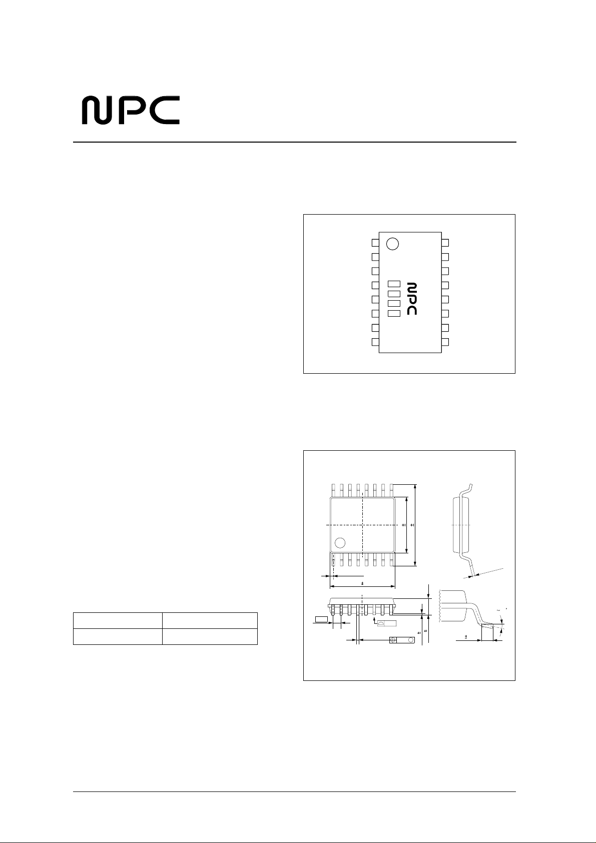
16-pin VSOP packages.
FEATURES
■
Stereo inputs and outputs
■
Attenuation function
• 2-channel independent control
• 1.0 dB/step over 80 steps
• 0 to − 80 dB range
■
Mute function
■
3-wire serial data control (MDT, MCK, MLEN)
■
Chip addressing (up to 4 devices can be connected
in parallel)
■
Low noise
• ≤ 0.002% THD + noise
• 10 µVrms residual noise
■
5 V single power supply
■
Silicon-gate CMOS process
APPLICATIONS
Audio Variable Volume IC
PINOUT
(T op V iew)
RSTN
1
ADRS1
ADRS2
DVDD
LOUT
LIN
AVDD
8
VRL VRR
PACKAGE DIMENSIONS
(Unit: mm)
16 pin VSOP
4.4 0.2
6.4 0.2
16
6451AV
MDT
MCK
MLEN
DVSS
ROUT
RIN
AVSS
9
■
Audio equipment
ORDERING INFORMATION
Device Package
SM6451AV 16-pin VSOP
0.65
0.275TYP
5.1 0.2
0.10
+ 0.10
0.22
- 0.05
M
0.12
0.10 0.05
NIPPON PRECISION CIRCUITS—1
1.15 0.1
0.5 0.2
0.15
+ 0.1
- 0.05
010
Page 2
BLOCK DIAGRAM
SM6451AV
DVDD DVSS
LIN
Attenuation
Control
1/2VDD
MLEN
MCK
MDT
Attenuation Decoder
Interface Control
Circuits
RSTN
Decoder
Address
ADRS1
Chip
ADRS2
1/2VDD
RIN
Attenuation
Control
AVDD AVSS
PIN DESCRIPTION
Number Name I/O
1 RSTN Ip D System reset input (LOW-level reset)
2 ADRS1 Ip D Chip address set 1
3 ADRS2 Ip D Chip address set 2
4 DVDD – D Digital supply
5 LOUT O A Left-channel audio output
6 LIN I A Left-channel audio input
7 AVDD – A Analog supply
8 VRL O A
9 VRR O A
10 AVSS – A Analog ground
11 RIN I A Right-channel audio input
12 ROUT O A Right-channel audio output
13 DVSS – D Digital ground
14 MLEN Ip D Microcontroller latch enable input
15 MCK Ip D Microcontroller clock input
16 MDT Ip D Microcontroller data input
1. Ip = input pin with pull-up, A = analog, D= digital
1
A/D
1
Left-channel reference voltage (0.5V
between VRL and AVSS.
Right-channel reference voltage (0.5V
between VRR and AVSS.
Reference
Voltage
LOUT
VRL
VRR
ROUT
Description
). Connect a 10 µF capacitor
DD
). Connect a 10 µF capacitor
DD
NIPPON PRECISION CIRCUITS—2
Page 3
−
−
SPECIFICATIONS
Absolute Maximum Ratings
−
SM6451AV
DVSS = AVSS = 0 V, DVDD = AVDD = V
DD
Parameter Symbol Rating Unit
Supply voltage V
Input voltage V
Power dissipation P
Storage temperature T
Soldering temperature T
Soldering time t
Recommended Operating Conditions
DVSS = AVSS = 0 V, DVDD = AVDD = V
Parameter Symbol Rating Unit
Supply voltage V
Supply voltage deviation DV
Operating temperature T
DD
DD
− AV
DC Characteristics
DD
IN
D
stg
sld
sld
DD
, DV
− AV
DD
SS
SS
opr
0.3 to 7.0 V
V
− 0.3 to V
SS
+ 0.3 V
DD
150 mW
55 to 125
255
10 s
4.5 to 5.5 V
±0.1 V
40 to 85
° C
° C
° C
DVDD = AVDD = V
= 4.5 to 5.5 V, V
DD
Parameter Symbol Condition
Data transfer stopped, MDT, MCK,
MLEN, RSTN, ADRS1, ADRS2 = V
ADRS1 = ADRS2 = 0V, 1.2 Vrms analog
input, ATT = 0 dB, data transfer active
IH
IL
I
V
IL
I
IH
IN
V
IN
DVDD Current consumption
AVDD Current consumption I
HIGH-level input voltage
LOW-level input voltage
Input current
1
Input leakage current
1
1
1
I
DDD1
I
DDD2
DDA
V
V
1. MDT, MCK, MLEN, RSTN, ADRS1, ADRS2
= 0 V, Ta = − 40 to 85 ° C
SS
Rating
Unit
min typ max
DD
– 0.3 1.0 µA
–12mA
– 4.5 8 mA
0.7V
DD
– – 0.3V
––V
DD
= 0 V – 230 400 µA
= V
DD
– – 1.0 µA
V
NIPPON PRECISION CIRCUITS—3
Page 4
AC Digital Characteristics
SM6451AV
DVDD = AVDD = V
= 4.5 to 5.5 V, V
DD
= 0 V, Ta = − 40 to 85 ° C
SS
Serial inputs (MDT, MCK, MLEN)
Parameter Symbol
MCK, MLEN rise time t
MCK, MLEN fall time t
MDT setup time t
MDT hold time t
MLEN setup time t
MLEN hold time t
MLEN LOW-level pulsewidth t
MLEN HIGH-level pulsewidth t
MDT
tMDS
tMDH
r
f
MDS
MDH
MCS
MCH
MEWL
MEWH
Rating
Unit
min typ max
– – 100 ns
– – 100 ns
50 – – ns
50 – – ns
50 – – ns
50 – – ns
50 – – ns
50 – – ns
0.5VDD
MCK
tMCS
tMEWL
tf tr
MCK
MLEN
0.9VDD
0.1VDD
Reset input (RSTN)
Parameter Symbol
RSTN LOW-level pulsewidth t
RSTN
tMCH
tMEWH
0.5VDD
0.5VDDMLEN
0.9VDD
0.1VDD
Rating
min typ max
100 – – ns
0.5VDD
Unit
NIPPON PRECISION CIRCUITS—4
Page 5

Ω
SM6451AV
AC Analog Characteristics
V
= 5.0 V, 1.2 Vrms amplitude, 1 kHz input frequency, 100 k Ω output load resistance, Ta = 25 ° C,
DD
AC-coupled inputs
Analog inputs (LIN, RIN)
−
−
Parameter Symbol Condition
Rating
min typ max
Input reference amplitude V
Input resistance R
Input clipping voltage V
AI
IN
CLP
THD + N = 1%, ATT = 0 dB – 1.75 – Vrms
– 1.2 – Vrms
40 50 60 k
Analog outputs (LOUT, ROUT)
Parameter Symbol Condition
min typ max
Residual noise voltage V
NS
Signal-to-noise ratio SNR 95 100 – dBr
Total harmonic distortion + noise THD + N
Gain control range R
CNT
Input signal: 0 Vrms,
A-weight filter, 0 dBr = 1.2
Vrms, ATT = 0 dB
ATT = 0 dB, 20 kHz
lowpass filter
–1020 µ Vrms
– 0.0017 0.0025 %
80 – 0 dB
Step size Step 0.8 1 1.5 dB
Attenuation error (1k to 20kHz)
ERR
ERR
AT
0
AT
2
Absolute attenuation (1 kHz)
AT
4
AT
6
AT
8
Mute attenuation (1 kHz) Mute ATT = Mute
Channel crosstalk CT ATT = 0 dB
0 to − 60 dB
1
2
61 to − 80 dB
ATT = 0 dB –
ATT = − 20 dB –
ATT = − 40 dB –
ATT = − 60 dB –
ATT = − 80 dB –
− 2– 1dB
− 5– 0dB
− 88
− 105
Frequency response FR ATT = 0 dB, f = 200 kHz –
Quiescent output zip noise voltage
(while ATT value adjusting)
Minimum driver load resistance R
N
J
ML
0 Vrms input – – 3 mV
ATT = 0 dB, THD + N = 1% – 6 10 k Ω
Rating
− 0.1 – dB
− 20.1 – dB
− 40.3 – dB
− 60.5 – dB
− 83.0 – dB
− 92 – dB
− 112 – dB
− 5–dB
Unit
Unit
Reference voltage (VRL, VRR)
Parameter Symbol Condition
Reference voltage output V
REF
Rating
min typ max
0.45V
0.5V
DD
DD
NIPPON PRECISION CIRCUITS—5
0.55V
Unit
DD
V
Page 6

MEASUREMENT CIRCUIT
Chip address: ADRS1 = LOW, ADRS2 = LOW
SM6451AV
330pF
+
0.022uF10uF
+
0.022uF10uF
+
1uF
+
1uF
+
1 RSTN
2 ADRS1
3 ADRS2
4 DVDD
5 LOUT
6 LIN
7 AVDD
8 VRL
0.022uF10uF 0.022uF 10uF
Generator Analyzer
Audio Precision
System One SYS − 322A
MDT 16
MCK 15
MLEN 14
SM6451
DVSS 13
ROUT 12
RIN 11
AVSS 10
VRR 9
+
CPU
+
1uF
+
1uF
100kΩ100kΩ
NIPPON PRECISION CIRCUITS—6
Page 7

SM6451AV
MICROCONTROLLER INTERFACE
The SM6451AV uses a 3-wire serial interface comprising MDT (data), MCK (clock) and MLEN (latch
enable) to select channels and attenuation levels for the addressed device.
Input Timing
The microcontroller data input timing is shown in figure 1.
D15 D14 D13 D12 D11 D10 D9 D8 D7 D6 D5 D4 D3 D2 D1 D0MDT
MCK
MLEN
Figure 1. Microcontroller data input timing
Data is shifted into the internal shift register on the rising edge of MCK, and the attenuation value is updated
on the rising edge of MLEN. Accordingly, data on MDT should be changed on the falling edge of MCK. The
dotted lines for MCK and MLEN also indicate valid timing.
Note, however, a minimum of 16 MCK input pulses are required.
Data Format
The format of microcontroller input data is shown in figure 2.
MDT
D15, D14
Care
Don't
Care
Don't
Chip
Address 1
Chip
D15 D14 D13 D12 D11 D10 D9 D8 D7 D6 D5 D4 D3 D2 D1 D0
Care
Don't
Address 2
Care
Don't
Select
Channel
Select
Channel
Data 7
Attenuation
Figure 2. Microcontroller data format
Data 6
Attenuation
Attenuation
Data 5
Attenuation
Data 4
Attenuation
Data 3
Attenuation
Data 2
Attenuation
Data 1
Attenuation
Data 0
Don’t care.
D13, D12
Chip address bits. D13 corresponds to ADRS1 and D12 corresponds to ADRS2. The device is addressed only
when ADRS1:ADRS2 matches D13:D12.
Example 1: If D13 = LOW, D12 = HIGH and ADRS1 = LOW, ADRS2 = LOW, then the device is not
addressed since ADRS2 and D12 do not match.
Example 2: If D13/D12 = LOW and ADRS1/ADRS2 = LOW, then the device is addressed and all input data
is read and the attenuation settings updated.
D11, D10
Don’t care.
NIPPON PRECISION CIRCUITS—7
Page 8

SM6451AV
D9, D8
Channel select bits. The selected channel(s) are shown in table 1.
Table 1. Channel select
D9 D8 Selected channel
LOW LOW Both left and right channels
LOW HIGH Left channel
HIGH LOW Right channel
HIGH HIGH No change
D7 to D0
Attenuation register (ATT) set bits.
Table 2. Attenuation setting
Attenuation ATT
0 dB 00 LOW LOW LOW LOW LOW LOW LOW LOW
−1 dB 01 LOW LOW LOW LOW LOW LOW LOW HIGH
−2 dB 02 LOW LOW LOW LOW LOW LOW HIGH LOW
: :::::::::
−15 dB 0F LOW LOW LOW LOW HIGH HIGH HIGH HIGH
−16 dB 10 LOW LOW LOW HIGH LOW LOW LOW LOW
−17 dB 11 LOW LOW LOW HIGH LOW LOW LOW HIGH
: :::::::::
−63 dB 3F LOW LOW HIGH HIGH HIGH HIGH HIGH HIGH
−64 dB 40 LOW HIGH LOW LOW LOW LOW LOW LOW
−65 dB 41 LOW HIGH LOW LOW LOW LOW LOW HIGH
: :::::::::
−79 dB 4F LOW HIGH LOW LOW HIGH HIGH HIGH HIGH
−80 dB 50 LOW HIGH LOW HIGH LOW LOW LOW LOW
Mute 51 LOW HIGH LOW HIGH LOW LOW LOW HIGH
Mute 52 LOW HIGH LOW HIGH LOW LOW HIGH LOW
: :::::::::
Mute FE HIGH HIGH HIGH HIGH HIGH HIGH HIGH LOW
Mute FF HIGH HIGH HIGH HIGH HIGH HIGH HIGH HIGH
1. Outputs are muted after system reset.
1
H
D7 D6 D5 D4 D3 D2 D1 D0
NIPPON PRECISION CIRCUITS—8
Page 9

SM6451AV
ANALOG PERFORMANCE CHARACTERISTICS
DVDD = AVDD = 5.0 V, 100 kΩ output load resistance, Ta = 25 °C
1
0.1
THD + N(%)
0.01
0.001
0.1
VIN(Vrms)
f = 1kHz
ATT = 0dB
20kHz LPF
21
0.1
VIN=0.2Vrms
0.01
THD + N(%)
VIN=0.4Vrms
VIN=0.8Vrms
VIN=1.2Vrms
0.001
20 20k100 1k 10k
Freq(Hz)
Figure 3. THD + N vs. input amplitude Figure 4. THD + N vs. input frequency
2
1
0
−1
−2
Error(dB)
−3
−4
VIN = 1.2Vrms
f = 1kHz
20
16
12
Noise (uV)
8
4
ATT = 0dB
20kHz LPF
VIN = 0Vrms
A-Weight Filter
−5
0 −20−10 −30 −50 −60 −70 −80−40
ATT(dB)
Figure 5. Attenuation error Figure 6. Residual noise vs. ATT
ATT=0dB
+0
ATT=−20dB
−20
ATT=−40dB
−40
ATT=−60dB
Gain(dB)
−60
ATT=−80dB
−80
ATT=MUTE
−100
20 100 1k 10k 100k
VIN = 1.2Vrms
Freq(Hz)
Figure 7. Frequency response Figure 8. Crosstalk frequency response
0
0 −10 −20 −30 −40 −50 −60 −70 −80
ATT(dB)
−40
−60
−80
−100
Cross Talk Gain(dB)
−120
−140
20 100 1k 10k 100k
VIN = 1.2Vrms
ATT = 0dB
Freq(Hz)
NIPPON PRECISION CIRCUITS—9
Page 10

SM6451AV
+0
−20
−40
−60
−80
FFT Gain(dB)
−100
−120
−140
−160
0 20k2k 4k 6k 8k 10k 12k 14k 16k 18k
Freq(Hz)
Figure 9. FFT plot (ATT = 0 dB) Figure 10. THD + N vs. load resistance
10
AVDD + DVDD
8
6
ADRS1=ADRS2=5V
VIN = 1.2Vrms = 0dB
f = 1kHz
ATT = 0dB
BH window
100
10
1
0.1
THD + N(%)
0.01
0.001
1k
10
8
6
10k
Load resistance(Ω)
AVDD + DVDD
ADRS1=ADRS2=5V
VIN = 1.2Vrms
f = 1kHz
ATT = 0dB
20kHz LPF
100k
4
Current consumption(mA)
2
4.50 4.75 5.00 5.25 5.50
Supply volutage(V)
4
Current consumption(mA)
2
−50 −25 0 25 50 75 100
Operating temperature(°C)
Figure 11. Current consumption vs. supply voltage Figure 12. Current consumption vs. temperature
NIPPON PRECISION CIRCUITS—10
Page 11

SM6451AV
TYPICAL APPLICATIONS
Connection Guidelines
Decoupling capacitors of approximately 10 µF should be connected from AVDD, VRL, VRR to AVSS, and
from DVDD to DVSS.
In addition, approximately 0.01 µF capacitors should also be connected from AVDD, VRL, VRR to AVSS,
and from DVDD to DVSS to suppress digital switch noise.
An approximately 0.001 µF capacitor connected from RSTN to DVSS will force a system reset when power
is applied.
Connection 1 (to DAC)
+ 5V
DVDD
SM5864
DVSS
AVDD1 to 4
LOA
LOBN
ROA
ROBN
AVSS1 to 4
Analog L.P.F.
Analog L.P.F.
CPU
DVDD
LIN
RIN
SM6451
ADRS1
ADRS2
MDT MCK MLEN
MDT MCK MLEN
ADRS1
ADRS2
SM6451
LIN
RIN
AVSS
AVDD
LOUT
ROUT
DVSS
AVSS
AVDD
DVDD
LOUT
ROUT
DVSS
for Front
L ch OUT
R ch OUT
for Rear
L ch OUT
R ch OUT
NIPPON PRECISION CIRCUITS—11
Page 12

Connection 2
SM6451AV
L ch Input
3.3R
4Vrms 1.2Vrms
3.3R
R ch Input
R
LIN LOUT
R
SM6451
RIN ROUT
R
R
3.3R
L ch Output
3.3R
R ch Output
The SM6451AV uses a 1.2 Vrms input reference amplitude. If the input signal is 4 Vrms, then the input must
be reduced by a factor of 1/3.3, and the output increased by a factor of 3.3.
Connection 3
AVDDAVDD
L ch Input
LIN LOUT
L ch Output
SM6451
R ch Input
RIN ROUT
AVSS
R ch Output
When there is a possibility that the input peak-to-peak amplitude will exceed the supply voltage, input pro-
tection diodes should be connected to prevent device breakdown.
NIPPON PRECISION CIRCUITS INC. reserves the right to make changes to the products described in this data sheet in order to
improve the design or performance and to supply the best possible products. Nippon Precision Circuits Inc. assumes no responsibility for
the use of any circuits shown in this data sheet, conveys no license under any patent or other rights, and makes no claim that the circuits
are free from patent infringement. Applications for any devices shown in this data sheet are for illustration only and Nippon Precision
Circuits Inc. makes no claim or warr anty that such applications will be suitab le for the use specified without further testing or modification.
The products described in this data sheet are not intended to use for the apparatus which influence human lives due to the failure or
malfunction of the products. Customers are requested to comply with applicable laws and regulations in effect now and hereinafter,
including compliance with export controls on the distribution or dissemination of the products. Customers shall not expor t, directly or
indirectly, any products without first obtaining required licenses and approvals from appropriate government agencies.
NIPPON PRECISION CIRCUITS INC.
NIPPON PRECISION CIRCUITS INC.
4-3, Fukuzumi 2-chome
Koto-ku, Tokyo 135-8430, Japan
Telephone: 03-3642-6661
Facsimile: 03-3642-6698
NC9704AE 1998.06
NIPPON PRECISION CIRCUITS—12
 Loading...