

Page 1
SM5M2
- 1 -
In the absence of confirmation by device specification sheets, SHARP takes no responsibility for any defects that may occur in equipment using any SHARP devices shown in catalogs, data books,
etc. Contact SHARP in order to obtain the latest device specification sheets before using any SHARP device.
DESCRIPTION
The SM5M2 is a CMOS 4-bit single-chip microcomputer operated on 3.0 V single power supply.
This microcomputer integrates 4-bit parallel
processing function, ROM, RAM, display RAM, 15stage divider, 2-kind of interrupt and 4-level of
subroutine stack. With a built-in LCD drive circuit
for a maximum of 136 elements, a 2-mode standby
function, voice synthesizer and a melody generator
circuit in a single chip, the SM5M2 permits the
design of system configuration with a minimum of
peripheral components. It can be used in a variety
of products from handheld equipment to electrical
appliances, such as hand held games with voice,
and also achieves low power consumption.
FEATURES
• ROM capacity :
3 072 x 8 bits (For main program)
64 k x 5 bits (For voice)
256 x 6 bits (For melody)
• RAM capacity :
130 x 4 bits
(including 34 x 4 bits
display RAM)
• Instruction sets : 51
• Subroutine nesting : 4 levels
• I/O port :
Input 1
Output 6
Input/output 7
• Interrupts :
Internal interrupt x 1 (divider overflow)
External interrupt x 1 (INTA)
• Built-in voice synthesizer circuit (APCM) :
Number of phrases : 256
Voice ROM : 64 k x 5 bits
Bit rate : 25/35 kbps
Number of coded bit : 5 bits
Sampling frequency : 5/7 kHz
Generation period : 9.1 to 12.8 s
• Built-in main clock oscillator for system clock
• Built-in sub clock oscillator for real time clock
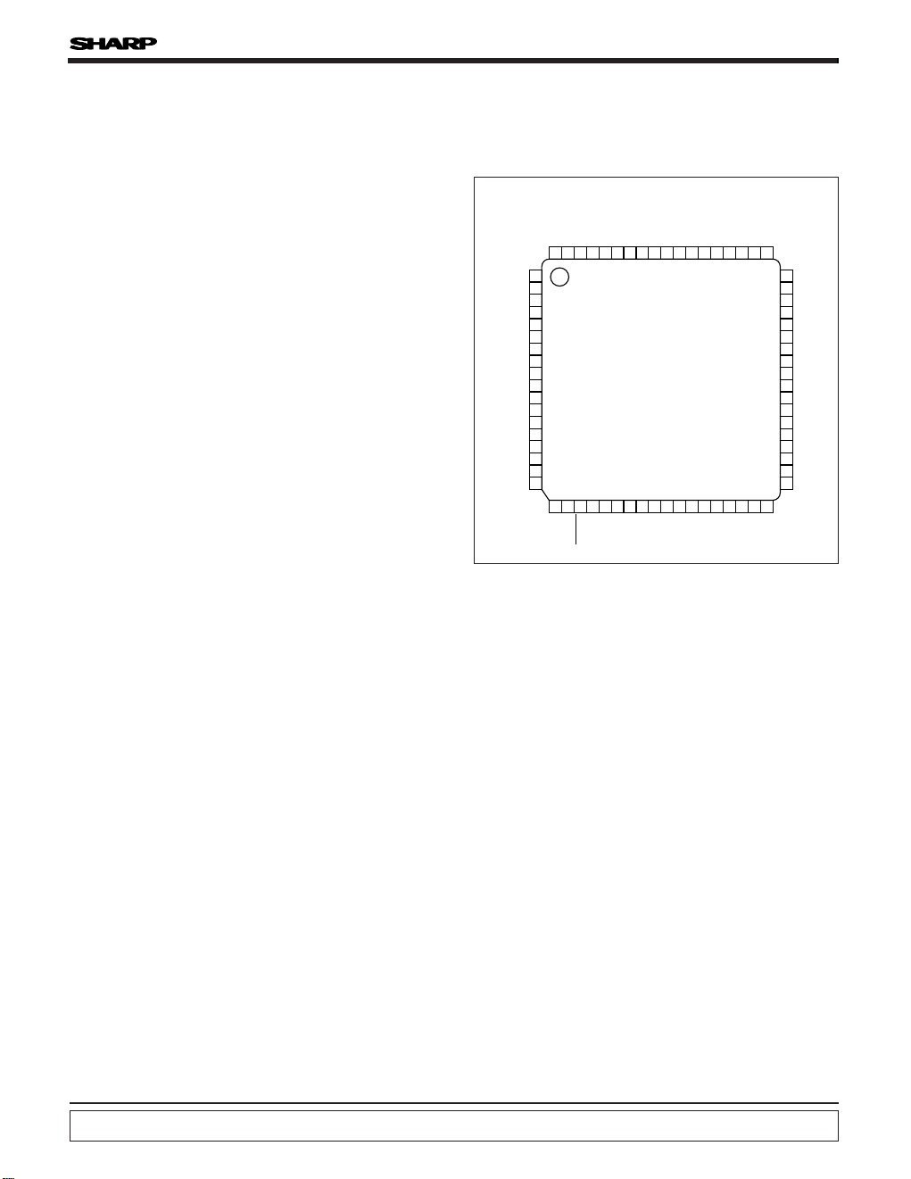
PIN CONNECTIONS
• Built-in 15 stages divider for real time clock
• Built-in LCD driver :
136 segments, 1/2 bias, 1/4 duty cycle
• Built-in melody generator circuit :
Melody ROM : 256 steps
Generating time (at 32.768 kHz) : 32 s (MAX.)
• Instruction cycle time :
25.9 µs (MIN.) (at 70 kHz ± 10%)
61 µs
∗
(TYP.) (at 32.768 kHz)
∗
When using the clock with the system clock.
• Standby function
• Supply voltage : 2.4 to 3.3 V
• Package : 72-pin QFP (QFP072-P-1010)
1
2
3
4
5
6
7
8
9
10
11
12
13
14
15
54
53
52
51
50
49
48
47
46
45
44
43
42
41
40
(NC)
S
25
S24
S23
S22
S21
S20
S19
S18
S17
S16
S15
S14
S13
S12
16
17
18
39
38
37
S
11
S10
(NC)
19 20 21 22 23 24 25 26 27 28 29 30 31 32
33
72 71 70 69 68 67 66 65 64 63 62 61 60 59
58
34 35
36
57 56
55
GND1
VOA
RESET
V
DD2
CK2
CK1
TOSC
S
0
S1
GND
S
2
S3S4S5S6S7S8S9
(NC)
VOCS
OSC
OUT
OSCIN
VDSP
H0H1H2H3
GND
S33S32
S31
S30
S29
S28
S27
S26
INTA
(NC)
P0
0
P01
P02
P03
P10
P11
P12
P13
P20
P21
P22
T
F
VOICE
VR
V
DD
SM5M2
4-Bit Single-Chip Microcomputer
(LCD Driver)
72-PIN QFP TOP VIEW
Page 2
SM5M2
- 2 -
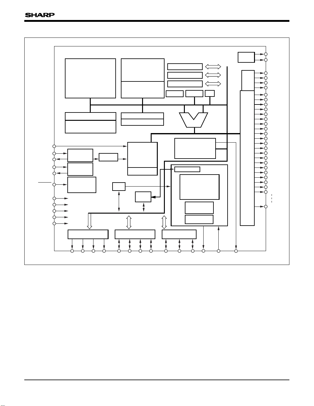
BLOCK DIAGRAM
RD
PC
B
SB
P0 P1 P2
SR x 4
RE
RF
A
CC XC
HC
RAM
96 x 4-bit
ROM
3 072 x 8-bit
DISP RAM
34 x 4-bit
ALU
LCD DRIVER
VDSP
VOA
H0
S0
H1
H2
H3
S1
S2
S3
S4
S5
S6
S7
S8
S9
S10
S11
S12
S13
S14
S15
S16
S17
S18
S19
S20
S33
GND
V
DD
VOSC
T
RESET
CK1
OSCOUT
OSCIN
INTA
F
P2
2P21P20P13P12P11P10P03P02P01P00
BLEEDER
MELODY
CONTROLLER
MELODY ROM
6 x 256-STEP
INTERRUPT
CONTROLLER
OSC
VOICE ROM
5 x 64 k-STEP
VOICE FLAG
EXPANDER
D/A
CONVERTER
5 to 8-bit
VOICE VR
DIVIDER
RC
P33
HARDWARE
RESET
CIRCUIT
OSC2
FOR LCD
REAL TIME CLOCK
OSC1
FOR
VOICE
SYSTEM CLOCK
CK2
VOICE ROM START ADDRESS
TOSC
IFA
IFD
Nomenclature
ACC : Accumulator
ALU : Arithmetic logic unit
B : RAM address register
C : Carry flag
HC : Common signal generator circuit
IFA : External interrupt flag
IFD : Divider overflow flag
RC : Voice starting address
OSC
IN,
OSC
OUT : Oscillator for LCD and real time clock
P0-P2 : Port registers
P3
3 : Voice flag port
PC : Program counter
RAM : Data memory
RD, RE, RF : Mode registers
ROM : Program memory
SB : Stack B register
SR : PC stack register
X : X register
CK
1,CK2 : Oscillator for voice and system clock
Page 3
SM5M2
- 3 -
P00-P03
PIN DESCRIPTION
PIN NAME I/O FUNCTION
GND, VDD, VDSP, VR I
Power supply pins. The VDD, VDSP, VR pins apply a positive supply with respect
to the GND.
T, TOSC, VOSC I
LSI chip test pins. Cannot be used by the user. Connect T and TOSC to GND.
Connect VOSC to VDD.
RESET I
Input pin with built-in pull-up resistor. Hardware-reset the LSI chip when a Low
level signal is input. Normally, a capacitor is connected between it and GND to
form a power-on reset circuit.
OSCIN, OSCOUT I/O
I
O
Crystal oscillator pins. Connect a crystal oscillator accross [OSCIN-OSCOUT ] to
form a clock generator circuit.
RC oscillator pins. Connect a resistor across [CK1-VDD ] to form a clock generator
circuit. CK
2 is used to test its clock out.
Voice output pin. Output the contents of a voice ROM.
F
CK1, CK2
Voice
O
Melody output pin. Outputs the contents of a melody ROM with standard 12
musical scales (555 to 2 114 Hz) in two octaves.
H0-H3 O Pins for the LCD's common signals.
S0-S33 O Pins for the LCD's segment signals.
INTA I Input pin for external interrupt. The IFA flag is set at the rising edge of INTA.
O
Output ports. The P0 ports are an output port. The accumulator ACC can be
transferred to this port by instruction.
P10-P13, P20-P22 I/O
P1 and P2 are I/O pins which can switch to input or output pins in 4/3-bit units
by instruction. They can be used as output pins when configured for a key
matrix. The SM5M2 is forced to hardware-reset when all of P1
0-P13 pins are High
level. (By mask option)
Page 4
SM5M2
- 4 -
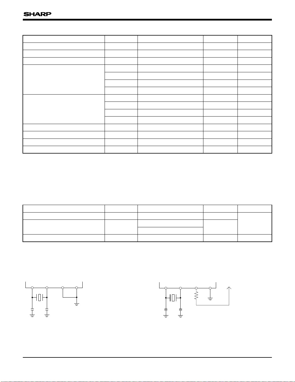
ABSOLUTE MAXIMUM RATINGS
PARAMETER SYMBOL RATING UNIT NOTE
Supply voltage VVDD – 0.3 to 4.0
Input voltage VI – 0.3 to VDD + 0.3 V
Output voltage VO –0.3 to VDD + 0.3 V
Source output current for each pin
IO1 2 mA 1
IO2 2 mA 2
IO3 2 mA 3
IO4 2 mA 4
Sink output current for each pin
IO5 2 mA 1
IO6 100 µA 2
IO7 2 mA 3
IO8 2 mA 4
Total source output current IOH 10 mA
Total sink output current IOL 10 mA
Operating temperature TOPR 0 to 50
°C
Storage temperature TSTG –55 to 150
°C
NOTES :
1. Applicable pins : P00-P03
2. Applicable pins : P10-P13, P20-P22
3. Applicable pin : F
4. Applicable pins : H
0-H3, S0-S33
NOTE :
1. Use the crystal oscillation circuit
RECOMMENDED OPERATING CONDITIONS
Oscillation Circuit
OSCIN
OSCOUT CK1 CK2
Crystal
C
1 C2
R
OSCIN
OSCOUT CK1 VDDCK2
Crystal
C
1 C2
NOTE :
Mount the R, C and crystal as close to the LSI chip as possible to minimize the effects of stray capacitance.
PARAMETER SYMBOL RATING UNIT NOTE
Supply voltage VVDD 2.4 to 3.3
Instruction cycle TSYS
Crystal+CR 25.9 to 31.7
Crystal 61.0
µs
Oscillation starting voltage VOSC 2.0 V 1
• Crystal oscillation (frequency = 32.768 kHz)
• CR oscillation (frequency = 70 kHz)
NOTE: In case of using RC resonator, crystal is also required.
Crystal : 32.768 kHz
C
1 = 15 pF
C
2 = 15 pF
Degree of fluctuation frequency : ± 10%
(V
DD = 3 V, TOPR = 25°C)
C
1 = 15 pF, C2 = 15 pF, R = 1.0 MΩ
Page 5
SM5M2
- 5 -
DC CHARACTERISTICS (VDD = 2.4 to 3.3 V, TOPR = 0 to +50°C)
PARAMETER
SYMBOL CONDITIONS
MIN. UNIT NOTE
Input voltage
VIH1 0.8 x VDD VDD
V 1
VIL1 0 0.2 x VDD
VIH2
V
DD
–0.25
VDD
V 2
VIL2 0 0.25
Input current
IIH1 VIH = VDD 30.0
µA
3
IIH2 VIH = VDD 30.0 4
IIL1 VIL = 0 V 25.0
5
10
11
-IOH1
IOL1
VOH = VDD – 0.5 V
VOL = 0.5 V
VOH = VDD – 0.5 V
VOL = 0.5 V
500
1 000
500
25
1 300
2 000
1 300
90.0
980
740
200
µA
6
-IOH2
IOL2
Output current
IO1 D= 1FH
7
IO2 D= 0FH
IO3 D= 01H
8
IOP11 CRRUN1 120 150
IOP12 CRRUN2 110 130
9
ISt11 CRSTOP1 15.0
4.00
3.00
50.0
40.0
30.0
26.0
26.0
4.0
15
30
40.0
15.0
13.0
100.0
80.0
60.0
52.0
52.0
15.0
Supply current
ISt12 CRSTOP2
CRSTOP3
XTALRUN1
XTALRUN2
XTALHALT1
XTALHALT2
XTALHALT3
XTALSTOP
VDD=3.0 V
VDD=3.0 V
µA
kΩ
ISt13
IOP21
IOP22
ISt 21
ISt 22
ISt 23
ISt 24
DCOM
DS
NOTES :
1. Applicable pins : P10-P13, P20-P22
2. Applicable pins : OSCIN, RESET, T, INTA
3. Applicable pins : P2
0-P22
4. Applicable pins : P10-P13
5. Applicable pin : RESET
6. Applicable pins : P0
0-P03, F
7. Applicable pins : P1
0-P13, P20-P22
8. Applicable pins : VOICE, value of external resistor = 2 kΩ
9. Measurement conditions in detail are mentioned in the
tables next page.
10. Applicable pins : H
0-H3
11. Applicable pins : S0-S33
VDD
VOA
GND
LCD wave form (EXAMPLE)
MAX.TYP.
Output impedance
Page 6
SM5M2
- 6 -
STATUS
CRRUN1
CRRUN2
CRSTOP1
CRSTOP2
CRSTOP3
0 1 1 0 ON ON ON ON ON ON
0 1 0 ON ON ON OFF ON ON
0 1 0 OFF ON OFF OFF ON ON
0 0 0 OFF ON OFF OFF OFF ON
0 0 1 OFF ON OFF OFF OFF OFF
0
1
1
1
CR + X'TAL Standby Mode
STOP P33 RF1 RD2 CR X'TAL CPU Voice LCD Divider
STATUS
XTALRUN1
XTALRUN2
XTALHALT1
XTALHALT2
XTALHALT3
XTALSTOP
0 0 1 1 0 OFF ON ON ON ON ON
0 0 0 1 0 OFF ON ON OFF ON ON
0 1 0 1 0 OFF ON OFF OFF ON ON
0 1 0 0 0 OFF ON OFF OFF OFF ON
0 1 0 0 1 OFF ON OFF OFF OFF OFF
1 0 0 0 0 OFF OFF OFF OFF OFF OFF
Only X'TAL Standby Mode
STOP HALT P33 RF1 RD2 CR X'TAL CPU Voice LCD Divider
NOTES :
• When CR = OFF, CPU and Voice are OFF.
• When Divider = OFF, neither LCD nor Melody is in operation (undefined).
• STOP = 1 stands for executing STOP instruction.
• HALT = 1 stands for executing HALT instruction.
NOTES :
• When CR = OFF, CPU and Voice are OFF.
• When Divider = OFF, neither LCD nor Melody is in operation (undefined).
• STOP = 1 stands for executing STOP instruction.
Page 7
SM5M2
- 7 -
SYSTEM CONFIGURATION
A Resister and X Register
The A register (or accumulator : ACC) is a 4-bit
general purpose register. The register is mainly
used in conjunction with the ALU, C flag and RAM
to transfer numerical value and data to perform
various operations. The A register is also used to
transfer data between input and output pins.
The X register (or auxiliary accumulator) is a 4-bit
register and can be used as a temporary register.
It loads contents of the A register or its content is
transferred to the A register.
When the table reference instruction PAT is used,
the X and A registers load ROM data.
A pair of A and X registers can accommodate 8-bit
data.
7
3
0
003
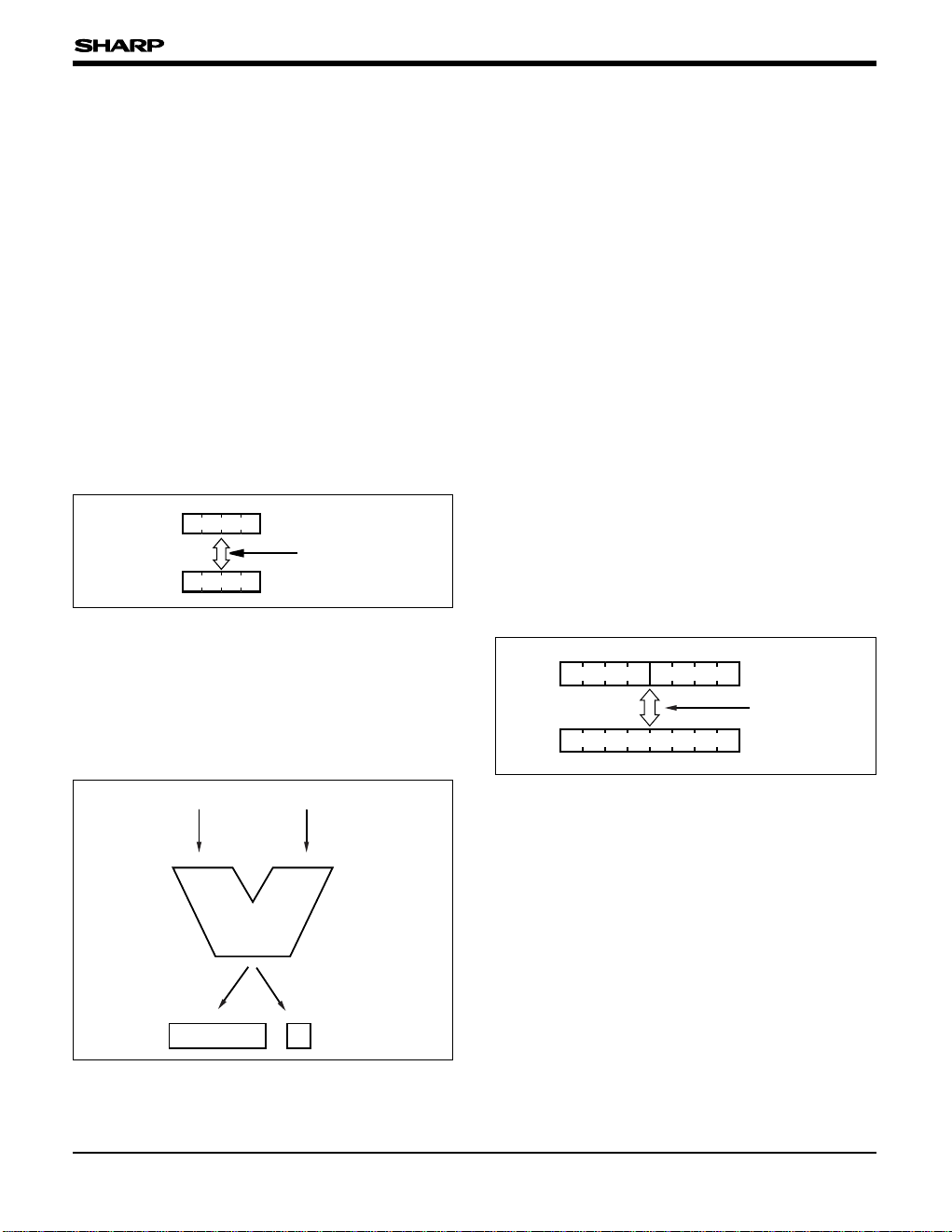
EX instruction (swap)
SB register
BM registerB register BL register
Fig. 1 Data Transfer Example Between
A Register and X Register
Arithmetic and Logic Unit (ALU) and
Carry Signal Cy
The ALU performs 4-bit parallel operation.
B Register and SB Register
• B register (BM, BL)
The B register is an 8-bit register that is used to
specify the RAM address.
The upper 4-bit section is called B
M register and
lower 4-bit B
L.
• SB register
The SB register is an 8-bit register used as the
save register for the B register. The contents of B
register and SB register can be exchanged through
EX instruction.
Fig. 3 B Register and SB Register
Fig. 2 ALU
The ALU operates binary addition in conjunction
with RAM, C flag and A register. The carry signal
Cy is generated if a carry occurs during ALU
operation. Some instructions use Cy : ADC
instruction sets/clears the content of the C flag;
ADX instruction causes the program to skip the
next instruction. Note that Cy is the symbol for
carry signal and not for C flag.
3
A register
3
X register
0
0
EXAX instruction
4-bit data 4-bit data
ALU
Result of operation
Areg
c
Page 8
SM5M2
- 8 -
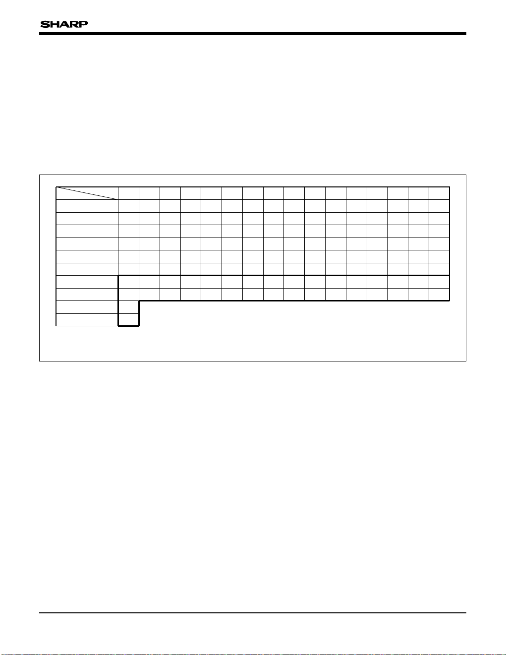
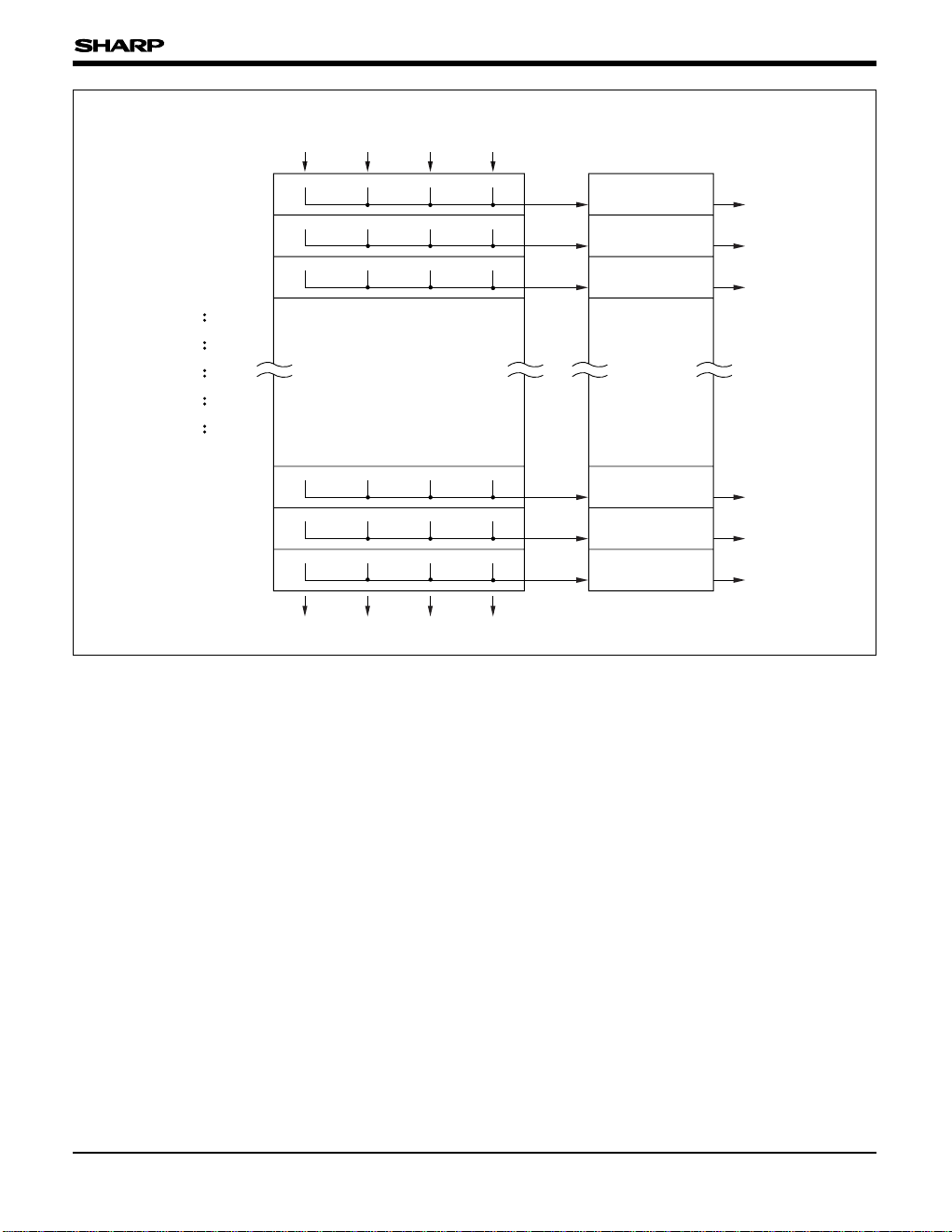
Data Memory (RAM)
The data memory (RAM) is used for data storage.
The RAM capacity consists of 130 x 4-bit (include
34 x 4-bit display RAM).
Display RAM, which outputs data to an external pin
for driving the segments of the LCD. Therefore, by
writing data to the display RAM, the LCD can be
driven at 1/4 duty (1/2 bias) to enable automatic
display of the LCD.
As shown in Fig. 5 the display RAM is connected
to segment outputs port from S
0 to S33 which
correspond to the LCD common outputs H
0 to H3.
Data M
0 to M3 for one column of the display RAM
is output pins as a LCD drive waveform which
corresponds to outputs H
0 to H3. As a RAM, the
display RAM operates exactly the same as other
RAMs.
0 1 2 3 4 5 6 7 8 9 A B C D E F
0
1
2
3
4
5
8 S0 S2 S4 S6 S8 S10 S12 S14 S16 S18 S20 S22 S24 S26 S28 S30
9 S1 S3 S5 S7 S9 S11 S13 S15 S17 S19 S21 S23 S25 S27 S29 S31
A S32
B S33
Fig. 4 RAM Organization
∗
The area surrounded by the thick line represents the display RAM where S
0 to S33 corresponds to the segment
output.
BM
BL
Page 9
SM5M2
- 9 -
Fig. 5 Relationship between The Display RAM and LCD Segment Outputs/Common Outputs
H3 H2 H1 H0
M3 M2 M1 M0
(RAM bit)
BM = 1000
(Register)
BL = 0000
BM = 1001
BL = 0000
BM = 1000
BL = 0001
BM Register
BM = 1000
LCD
Segment
S0
S1
S2
drive circuit
Common outputs
BM = 1001
BL = 1111
BM = 1010
BL = 0000
BM = 1011
BL = 0000
S31
S32
S33
Page 10

SM5M2
- 10 -
Program Counter PC and Stack Register SR
A ROM address is specified by the program
counter (PC). The PC comprises 12-bit where 6bit (P
U) are used to specify the page (see Fig. 6)
and 6-bit (P
L) are used to specify the step. PU is a
register and P
L is a binary counter.
The table reference instruction PAT executes a
similar operation to that of the subroutine jump and
uses one level of the stack register.
Program Memory (ROM)
The ROM is used for program storage. The ROM
capacity of the SM5M2 is 3 072-step . The ROM
is organized into 48-page where one page is
organized into 64-step.
Program counter PC
PU PL
Push Pop
SR ( level 1 )
SR ( level 2 )
SR ( level 3 )
SR ( level 4 )
MSB LSB
Stack register SR
Page Step
Fig. 6 Program Counter PC and Stack Register SR
Page 00H01H02H03H04H05H06H07H08H09H0AH0BH0CH0DH0EH0F
H
PU
000000
Program
start
First page
of
subroutine
TRS
Interrupt Standby
release
Table
reference
page PAT
000001 000010 000011 000100 000101 000110 000111 001000 001001 001010 001011 001100 001101 001110 001111
Page 10H11H12H13H14H15H16H17H18H19H1AH1BH1CH1DH1EH1F
H
PU
010000 010001 010010 010011 010100 010101 010110 010111 011000 011001 011010 011011 011100 011101 011110 011111
Page 20H21H22H23H24H25H26H27H28H29H2AH2BH2CH2DH2EH2F
H
PU
100000 100001 100010 100011 100100 100101 100110 100111 101000 101001 101010 101011 101100 101101 101110 101111
Last page
Fig. 7 ROM Organization
Page 11

SM5M2
- 11 -
SM5M2
INTA pin
Noise debounce circuit
To interrupt controller
To A
CC
Level
SM5M2
Output pin or I/O pin
set output
Output pin
Data bus of the
connected device
DON'T
Flags
The SM5M2 provides 4-flag (C flag and interrupt
request flag <IFA, IFD, P3
3>) which can be used to
set or determine conditions.
Output Latch Registers and Mode Registers
The output latch registers are connected to the P0,
P1 and P2 pins. By instruction, the contents of the
A
CC can be transferred to the output latch registers.
The SM5M2 also contains mode registers RC, RD,
RE and RF. Setting the value of each register
enables the voice start address, divider, LCD,
melody or interrupt to be controlled. Setting a
register is performed in the same way as the other
output pins. The functions of the mode registers
are shown in Table 1.
• INTA pin
INTA level can be loaded to A
CC (bit 0), as follows.
LBLX 4
IN
INTA level does not through the noise debounce
circuit.
CAUTION :
Connecting considerations of I/O port
When using an I/O port as bidirectional bus such as data
bus, avoid setting the I/O port to output when the target pin
is also set output.
Whenever the both output data conflict each other, system
failure will be caused due to damaged circuits or
instantaneous supply voltage drop.
Page 12

SM5M2
- 12 -
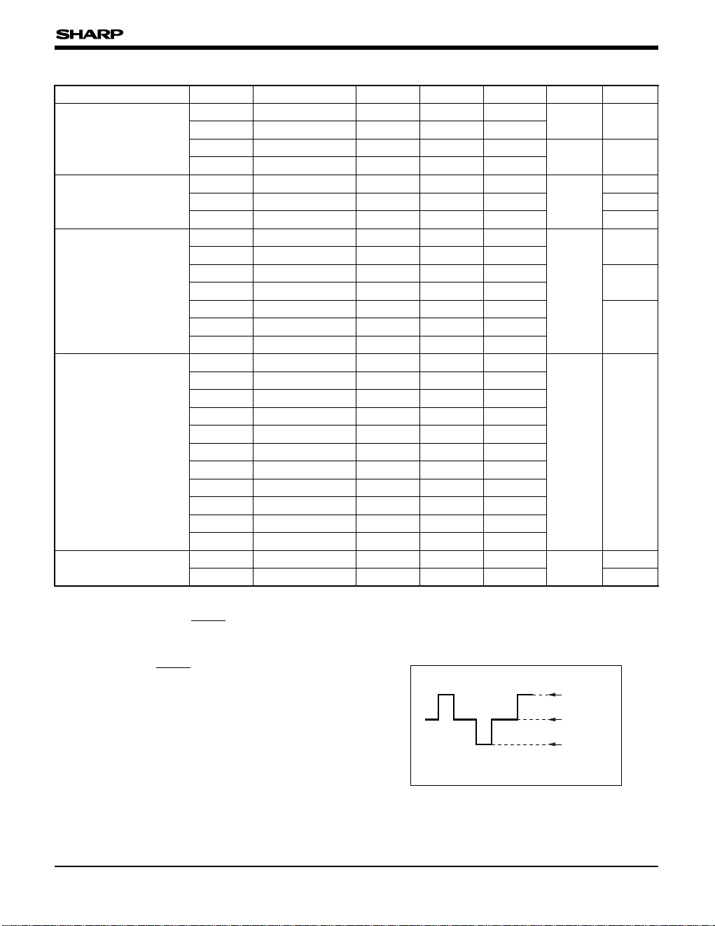
Table 1 Mode Register Setting
REGISTER
SET VALUE
MODE DESCRIPTION
TYPE BIT
RD
RC
RD0
RC0
RC7
0
–
Clears the ME F/F to stop a melody.
Sets voice synthesizer starting address.
1 Sets the ME F/F to start a melody from a ROM pointer address.
RD2
RD1
1
1
0
0
Masks divider clock-in.
Sets voice synthesizer to 5 kHz sampling rate.
Accepts divider clock-in.
Sets voice synthesizer to 7 kHz sampling rate.
Sets by stop instruction (of melody code) and reset by TPB instruction.
RD3
RE
RE0
0 Masks the interrupt based on the IFA flag.
1 Accepts the interrupt based on the IFA flag.
RE1 – Sets "0" only.
RE2
0 Masks the interrupt based on the IFD flag.
1 Accepts the interrupt based on the IFD flag.
RE3 – No setting.
RF
RF0
0 Turns off the LCD.
1 Turns on the LCD.
RF1
0 Stops the function of a bleeder circuit.
1 Operates the function of a bleeder circuit.
RF2
0
Creates the system clock frequency by dividing two the main oscillation
frequency.
1
Creates the system clock frequency by dividing four the main oscillation
frequency.
RF3 – Sets "0" only.
–
Page 13

SM5M2
- 13 -
OSCIN
OSC
CG
OSCOUT
OSCIN-OSCOUT : Crystal oscillation
(32.768 kHz)
CK2
OSC
CK1
CK1-CK2 : CR oscillation
(70 kHz)
MPX.
f
SYS
fSYS = 17.5 kHz or 35 kHz
1
2
121
2
121212121212121212121212121
2
fC
f0f14
1 Hz
2 Hz
f
C = 1 Hz or 2 Hz
Determined by
mask option
4 kHz 2 kHz 256 Hz
RF2
Divider
Fig. 8 System Clock Generator and Divider
Either of the system clock frequencies 35 kHz or
17.5 kHz ( in case of CR oscillation) can be
selected by the RF2 flag (See Table 2). The 17.5
kHz clock has slower command execution speed,
but uses less power for the same function.
The system clock is initialized to 35 kHz after
hardware reset operation.
The Table 2 shows the relationship between the
contents of RF2 flag for OSC resonator and the
generated frequency, f
SYS.
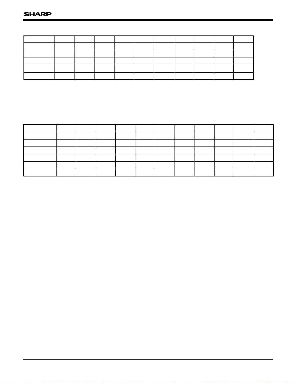
Table 2 OSC Resonator and Frequency fSYS
FOR OSC RESONATOR
CONTENTS OF RF2 FLAG
GENERATED FREQUENCY fSYS
70 kHz CR oscillation
0 35 kHz
1 17.5 kHz
32.768 kHz crystal
0 16.384 kHz
1 8.192 kHz
System Clock Generator and Dividers
The main oscillation frequency (CR oscillator) which
is input through CK
1 is divided into 2 or 4 to
generate the system clock f
SYS (Fig. 8).
System clock f
SYS determines the execution
instruction cycle so that the system clock period is
the same as the instruction cycle.
However, the instruction execution cycle of twoword instruction is twice that of one-word
instructions.
Use of a CR oscillating element or a crystal
oscillating element for the oscillator circuit is
determined by the mask option. The crystal
oscillator which is input through "OSC
IN-OSCOUT"
can be used as both real time clock and display
signal of LCD. On the final stage of the divider, fc
can be set 1 Hz or 2 Hz ( in case of 32 kHz crystal
oscillation) depending on the mask option.
Page 14

SM5M2
- 14 -
FUNCTIONAL DESCRIPTION
Voice Synthesizer
• How to select a voice start address
There is a voice start address and RC, composed
of 8-bit to select a voice start address. Voice start
address is 16 bits. However, RC register can points
only upper 8 bits in voice start address in partial.
Lower 8-bit is always fixed "0". Refer to "RC
register".
Minimum unit (shortest block) is equal voice ROM
capacity. Each minimum unit is composed of 256
steps. Refer to Fig.9.
Core CPU detects the status whether voice
synthesizer run or not, by reading the content of
P3
3 flag. (P33 flag is "1" during voice generation.)
Terminator (11111B) can be set as a voice data in
the voice ROM.
When controller found a terminator, immediately
stops voice and reset a flag.
When reached the bottom of the voice data
address, voice data address automatically becomes
0000
H and voice continuously generates until come
across a terminator.
CPU can reset the P3
3 flag and stop voice
generation by force.
NOTE :
Voice ROM data "11111" means terminator of voice data.
That is, an encoder must encode voice data except "11111".
• Voice sampling frequency (5 kHz / 7 kHz)
In case of sampling frequency is 5 kHz, total
generation period becomes 12.8 s. In case of 7
kHz, it's 9.1 s.
Voice sampling frequency (5 kHz or 7 kHz) is
selected by RD3 register. In case of RD3 is "0",
voice sampling frequency becomes 7 kHz. In case
of RD3 is "1", it's 5 kHz.
• RC register
The RC register is composed of 8-bit. It can points
only upper 8 bits in the voice start address as
shown below. The data is filled with both A and X
registers.
NOTE :
A voice start address is corresponding to the RC register (8
bits). Maximum 256 (SM5M2) pieces of voice start address
can be selected. Each voice start address is based on
multiple number of 100H. When voice generates, P33 flag
becomes "1".
First set the sampling rate of the voice synthesizer.
The voice synthesizer start address is corresponding to the RC register and the 8 bits in the
RC register are obtained by A and X register. After
setting the P3
3 voice flag High, the voice
synthesizer would start playing. After detect P3
3
Low, the voice synthesizer could play the next
section of voice.
x15x14x13x12x11x10x9x8070605040302010
0
NOTE : "x" stands for "0" or "1"
•
Voice start address
Voice data
(Voice ROM)
Voice start
address
64k x 5 bits
Voice flag
0000H
0100H
0200H
0300H
0400H
0500H
0600H
0700H
X register Acc
70
Start address
7
3300
0
RC register (8 bits)
FF00H
Fig. 9 Voice ROM Configuration
Page 15

SM5M2
- 15 -
Melody Output Function
The built-in melody generation circuit provides a
variety of sound signals. Fig. 10 shows the block
diagram of the melody generating circuit.
The melody ROM can store notes, rest and stop
commands in 256-step
(1 step consists of 6-bit),
allowing the generation of 12-scale over two octaves
(555 to 2 097 Hz) and the section of the time base for
notes (125/62.5 ms).
1/2R1/2R1/2R1/2
R
8-bit preset binary counter
(Melody ROM address pointer)
Melody ROM address set
Melody ROM
256-step x 6-bit
f8
(128 Hz)
Decoder
RD1 flag
N-stage counterRD0 flag
Rest tell signal
Melody start/stop flag
F pin
16 Hz
8 Hz
Preset signal
Time base select signal
32.768 kHz
RD0 flag : Bit 0 of RD register
RD1 flag : Bit 1 of RD register
Fig. 10 Melody Generating Circuit
Page 16

SM5M2
- 16 -
CONTROL PROCEDURE
The binary counter for designating the address of
the melody ROM can be arbitrarily set using the
PRE instruction. A performance is started and
stopped by the RD0-flag to "1" and "0".
The stop code generates a "rest tell signal", and at
the same time, sets the RD1 flag. The end of the
melody can be found by testing the RD1 flag.
Accordingly, to stop a performance at the end of
melody, the RD0 flag must be clear upon detection
of RD1 flag = 1.
Next step of PRE instruction, put the NOP
instruction.
The following is an example of a melody
generating program.
MELO LAX 2
ATX
LAX 1
PRE ; Set the starting address of
the melody at the 21st.
Hexadecimal step.
NOP ; Dummy command
:
:
LBLX 0DH
LAX 1
OUT ; Start the melody
TPB 1 ; Executed for clear the
RD1 flag
NOP ; Dummy command
:
:
LBLX 0DH
L1 TPB 1 ; Test the RD1 flag
TR L1 ; Loop for detect the stop
code
LAX 0
OUT ; Stop the melody
Using these functions, the user can generate
music, sound effects, alarm signals, etc. as desired,
and any portion of the music can be repeated.
Table 3 lists the melody output frequencies. The
output frequency can be halved by making bit 5
(OCT) of the melody ROM Low (0). In Table 3, m
0
to m3 show data in bits 1 to 4 of the melody ROM.
Table 3 Melody Output Frequency
∗
1 Number of clocks for one cycle
∗
2 The number (n) in the waveforms represents the number of periods of the oscillation frequency (32.768 kHz) from the crystal
oscillator for the duration in that particular part of the waveform.
m3 m2 m1 m0
OUTPUT FREQUENCY (Hz)
CLOCK NUMBER
∗1
∗2
do 0 0 1 0 2114.1 15.5
si 0 0 1 1 1985.9 16.5
la# 0 1 0 0 1872.4 17.5
la 0 1 0 1 1771.2 18.5
sol# 0 1 1 0 1680.4 19.5
sol 0 1 1 1 1560.4 21.0
fa# 1 0 0 0 1489.5 22.0
fa 1 0 0 1 1394.4 23.5
mi 1 0 1 0 1310.7 25.0
re# 1 0 1 1 1236.5 26.5
re 1 1 0 0 1170.3 28.0
do# 1 1 0 1 1110.8 29.5
7
8
8
8
8
8
8
9
8
9
9
9
9
9
9
10
9
10
10
10
10
11
10
11
11
11
11
11
11
12
12
12
12
13
12
13
13
13
13
14
14
14
14
14
14
15
15
15
Page 17

SM5M2
- 17 -
MELODY ROM INSTRUCTION
The melody ROM instruction is composed of 6-bit.
This 6-bit instruction (1 set), corresponding to a
musical note, generates a sound signal.
l : Control the tone length. When “1”,
125 ms; when “0”, 62.5 ms.
OCT : When the octave is “1”, the frequency
is determined by m
3 -m0.
When the octave is “0”, 1/2 of the
frequency determined by m
3-m0.
m
3 - m0 : Frequency as shown in Table 3.
Pause when m
3 = m2 = m1 = m0 = 0,
stop instruction when m
3 = m2 = m1
= 0, m0 = 1.
l OCT m
3
m
2
m1m
0
MUSICAL SCALE TONE LENGTH
(ms) OCT m3 m2 m1 m0
sol 375 00111
la 125
sol 250
mi 250
do 375
re 125
do 250
la 250
00101
00111
01010
10010
11100
10010
00101
ADDRESS
DATA
MUSICAL NOTE INSTRUCTION
00 00 pause
01 27
02 27
03 27
04 25
05 27
06 27
07 2A
sol
sol
sol
la
sol
sol
mi
08
09
0A
0B
0C
0D
0E
0F
10
11
2A
22
22
22
3C
22
22
25
25
01
mi
do
do
do
re
do
do
la
la
stop
The tone length of an initial musical note which is
generated from ROM addressed data assigned by
a PRE instruction has an error of maximum ±4 ms.
Therefore, by applying a pause as an initial note, a
melody performs with a precisely regulated tone
length.
EXAMPLE OF WRITING ON THE MELODY ROM
An example of writing a tone such as the following,
on the melody ROM will be shown.
Page 18

SM5M2
- 18 -
Standby Function
A standby function is available which temporarily
stops program execution to conserve power
consumption. The state during which a program is in
execution is called the operation mode and the state
during which the execution is temporarily stopped is
called the standby mode.
Either CR or X' TAL oscillator can be selected to a
system clock generator circuit of SM5M2. Each
standby mode between CR+X' TAL and only X'TAL
is entirely different as tables shown below.
In case of CR+X' TAL oscillator, HALT instruction can
NOT
be used, only STOP instruction is available.
On the other hand, in case of only X' TAL oscillator,
both HALT and STOP instruction are available.
STATUS
CRSTOP1
CRSTOP2
CRSTOP3
0 1 0 OFF ON OFF OFF ON ON
0 0 0 OFF ON OFF OFF OFF ON
0 0 1 OFF ON OFF OFF OFF OFF
1
1
1
NOTES :
• When CR=OFF, CPU and Voice are OFF.
• When Divider=OFF, neither LCD nor Melody is in operation (undefined).
• STOP=1 stands for executing STOP instruction.
Table 4 CR+X'TAL Standby Mode
STOP HALT P33 RF1 RD2 CR
Standby mode Register status Chip's status
X' TAL CPU Voice LCD Divider
STATUS
XTALHALT1
XTALHALT2
XTALHALT3
XTALSTOP
1 0 1 0 OFF ON OFF OFF ON ON
1 0 0 0 OFF ON OFF OFF OFF ON
1
0
0 0 1 OFF ON OFF OFF OFF OFF
0
0
0
0 0 0 OFF OFF OFF OFF OFF OFF1
NOTES :
• When CR=OFF, CPU and Voice are OFF.
• When Divider=OFF, neither LCD nor Melody is in operation (undefined).
• STOP=1 stands for executing STOP instruction.
• HALT=1 stands for executing HALT instruction.
Table 5 Only X' TAL Standby Mode
STOP HALT P33 RF1 RD2 CR
Standby mode Register status Chip's status
X' TAL CPU Voice LCD Divider
To get a condition mentioned in the first to the sixth
boxes from right hand side, one of STOP or HALT
instruction must be executed under the condition
mentioned in the fourth to the sixth boxes from left
hand side.
For instance, to get the status of XTALHALT1, of which
contents are CR =OFF, X' TAL = ON, CPU=OFF,
Voice =OFF, LCD= ON, and Divider = ON in the only
X'tal standby mode, HALT instruction must be
executed under the condition of P3
3
= 0, RF1=1 and
RD2 =0.
NOTE :
The halt mode stops only system clock generator circuit.
This mode is used to activate the system immediately after
a condition causes a release to the operation mode.
Page 19

SM5M2
- 19 -
TRANSITION FROM THE OPERATION MODE TO THE
STANDBY MODE
The HALT instruction is executed to set the halt
mode and the STOP instruction is executed to set
the stop mode.
Since the interrupt is used to release from the
standby mode, the mode does not transfer to the
standby mode if any of the following conditions are
satisfied during execution of the STOP or HALT
instruction.
a) RE0 is set and the INTA level is High.
b) RE2 is set and the IFD flag is set.
If any of the conditions above is satisfied, the
mode does not transfer to the standby mode even
if the STOP or HALT instruction is executed and
the instruction at the address following that of the
STOP or HALT instruction is executed. Therefore,
place the JUMP instruction which specifies step 0
on page 3 to the location at the address following
that of the STOP or HALT instruction.
RELEASE FROM THE STANDBY MODE TO THE
OPERATION MODE
Release based on an interrupt request from the
INTA pin or divider overflow. However, the reset or
any port High in Port 1 is limited to a nonmaskable
interrupt request.
The program restarts from step 0 on page 3.
However, if the IME flag is set, the instruction at
step 0 on page 3 is executed and a subroutine
jump is performed to the interrupt processing
routine specified on page 2 according to the type
of interrupt.
Even if Low level input on INTA pin is removed
before 900 command cycles, the stop mode is
released.
However, the program will not jump to 20
H page
(interrupt process routine).
Interrupt request flag IFA is not set : the program
continues at step 0 of page 3.
Interrupts
Interrupts originate from an INTA input or divider
overflow. The IFA and IFD flags become interrupt
request flags.
The interrupt block is composed of mask flags
(RE0, RE2), the IME flag and interrupt processing
circuit.
As shown in Fig. 11, resetting a mask flag enables
the interrupt request flag to be independently
masked. Thus, the mask flags can be used in a
program to establish the interrupt priority. The
priority for interrupts generated simultaneously is
shown in Table 6.
During the standby mode, the contents of the RAM
and stack RAM are retained. The contents of the
flags, registers and output latches shown below are
also retained.
A release from the standby mode to the operation
mode is performed by a reset port input, an interrupt
from the nonmaskable INTA, any port High in Port 1,
and divider. A maskable interrupt request cannot
become a factor in releasing back to the operation
mode. The mask setting is performed with RE
register. (see Table 1)
CAUTION :
When all of P10 to P13 level are High, the SM5M2 is
performed to release the standby mode and enter normally
hardware reset operation. (Mask option)
FLAG
IFA flag
IFD flag
IME flag
C flag
P3
3 flag
REGISTER
ACC
X register
B
M, BL register
SB register
OUTPUT LATCH REGISTER
P0 register
P1 register
P2 register
SP
SR
RC, RD, RE, RF
Page 20

SM5M2
- 20 -
Table 6 Interrupt Event Summary
When the IME flag is set, the interrupt circuit
activates according to the interrupt request and a
subroutine jump is performed to the specified
address. The jump destinations according to
interrupt origin are shown in Table 6. When the
IME flag is cleared, an interrupt is not accepted
even if an interrupt request is generated. The
interrupt timing is shown in Fig. 12 and Fig. 13.
The timing chart shown in Fig. 12 shows the
interrupt enable state when an interrupt request
has been generated. In this case, the interrupt
processing signal INT goes High, one instruction
cycle after the interrupt request flag is set. When
INT goes High, the contents of the program
counter are pushed into the stack register and
execution jumps to the specified address. At this
time, the INT signal and the IME flag are cleared to
establish the interrupt disable mode. The IME flag
is set again when the RTNI instruction is executed
to establish the interrupt enable mode.
The timing chart shown in Fig. 13 shows the state
when interrupts are enabled while multiple
interrupts are generated. In this case, a subroutine
jump is performed according to the interrupt having
the highest priority. When returning from the
subroutine by executing the RTNI instruction, the
instruction (two words are executed for a two-word
instruction) at the location of return is executed and
the interrupt for the next highest priority is
accepted.
If an interrupt request is generated during execution
of a two-cycle instruction, the instruction is
executed after which interrupt processing is
performed. If consecutive LAX instructions are
skipped or if the SKIP conditions are satisfied, the
skip operation is terminated after which interrupt
processing is performed.
INTERRUPT REQUEST
(REQUEST FLAG)
JUMP DESTINATION PRIORITY
ORDER
INTERRUPT
ENABLE FLAG
PAGE STEP
INTA input (IFA) 2 0 1 RE0
Divider overflow (IFD) 2 4 2 RE2
IFA
IFD
IME
RE2 RE0
Stack register
Program counter
INT signal
Interrupt
processing
circuit
Interrupt enable flag
Interrupt request
flags
Mask flags
Fig. 11 Interrupt Block
Page 21

SM5M2
- 21 -
Fig. 12 Interrupt Timing Chart
Fig. 13 Interrupt Timing Chart
NOTE :
Fig. 12 and Fig. 13 show the case where the interrupt request flags are not masked.
System clock
Interrupt request flag
INT signal
Interrupt enable flag
Instruction cycle
Interrupt processing
routine
RTNI instruction
Interrupt
processing
routine
Instruction cycle
System clock
Interrupt request flag
Interrupt request flag
INT signal
Interrupt enable flag
Interrupt processing
routine
RTNI instruction
Interrupt processing
routine
Page 22

SM5M2
- 22 -
Hardware Reset Function
The hardware reset function mode activated two
instruction cycles after the falling edge from the
RESET pin. When the RESET pin is changed
from High to Low, the pulse which is input by the
OSC
IN pin is counted 2
15
times after which the reset
mode clears and the program counter starts from
address 0 on page 0.
The initialized status of the system after reset is
shown in Table 7.
The following reset functions are available.
• The I/O port is set as an input port and the mode
register RC, RD, RE and RF are cleared. The
output only port (P0) is cleared and output Low.
• The interrupt request flags (IFA, IFD) and the
interrupt enable flag (IME) are cleared and all
interrupts become disabled.
• The program counter start from step 0 on page 0.
For activate reset function, when power is turned
on, you must connect a capacitor (0.1 µF, TYP.)
across the RESET pin and GND.
Table 7 Reset Status
NOTES :
•
Undefined flags and registers should be initialized by software.
• When all of P1 pins (P10 to P13) level goes to High, the SM5M2 is performed to reset operation. (Mask option)
FLAG OR REGISTER, X-REGISTER STATUS ( in reset mode and at program start)
PC 0
SP Level 1
RAM Undefined
ACC Undefined
X-register Undefined
P0-P2 output latch registers 0
Divider 0
IFA flag 0
IFD flag 0
IME flag 0
0
C flag
P33 flag
Undefined
BM, BL registers Undefined
Register RC (bit 7-0)
Register RD (bit 1)
Register RD (bit 0)
0
Undefined
Register RE (bit 2, 1, 0) 0
Register RF (bit 3, 2, 1, 0)
Register RD (bit 3)
Register RD (bit 2)
0
0
0
0
Page 23

SM5M2
- 23 -
LCD Function
• Display segment
The SM5M2 contains a built-in circuit which directly
drive a 1/4 duty, 1/2 bias LCD.
A sample LCD pattern is shown in Fig. 14.
H3
H2
H1
H0
S2 S1 S0
S33 S32 S31 S30 S29 S28
Fig. 14 LCD Pattern
A segment of the LCD can be turned on or off by
setting the corresponding bit in the display RAM (see
Fig. 5) to "1" or "0". The displayed segments can
assume any configuration containing up to a
maximum of 136 segments. An example of a 7segment numeric display is shown in Fig. 15.
S1 S0
H0
H1
H2
H3
Fig. 15 Sample LCD Pattern for 7-Segment Numeric Display
• LCD drive waveforms
The LCD drive waveforms for the LCD pattern of
Fig. 15 displaying a "5" are shown in Fig. 16 (the
segment output uses S
0 and S1). For Fig. 16, 3 V
is applied to the V
DD pin, and 1.5 V is applied to
the V
OA pin.
T
H
0
VDD (3 V)
V
OA (1.5 V)
GND (0 V)
V
DD (3 V)
V
OA (1.5 V)
GND (0 V)
V
DD (3 V)
V
OA (1.5 V)
GND (0 V)
V
DD (3 V)
V
M (1.5 V)
GND (0 V)
V
DD (3 V)
V
OA (1.5 V)
GND (0 V)
V
DD (3 V)
V
OA (1.5 V)
GND (0 V)
H
1
H2
H3
S0
S1
Fig. 16 LCD Drive Waveforms
(frame frequency = 1/T = 64 Hz or 128 Hz)
∗
Frame frequency is selectable by mask option.
Page 24

SM5M2
- 24 -
VDD
RF1
SM5M2
R1
R1= R2
R2
VOA
VDD
• Blank display
There are two way to blank the entire display to
match the purpose.
(a) Blanking the display for a short time.
Set bit 0 of the RF register to "1" : Display
Set bit 0 of the RF register to "0" : Blank state
(b) Blanking the display for a long period mainy to
reduce supply current.
Set bit 0 and 1 of the RF register to "1" :
Display
Set bit 0 and 1 of the RF register to "0" :
Blank state
When bit 1 of the RF register is set "0", the voltage
(V
DD) applied to the bleeder resistors is turned off
and common outputs and segment outputs are
dropped to GND level so that the display blanks.
By cutting off the bleeder supply, the current
consumption can be greatly reduced. However,
when the display is blanked using method (b), the
response speed of the LCD returning to the display
state drops slightly. The RF register is in the blank
state after initialization (reset state) from hardware
reset.
Fig. 17 Booster Circuit
SM5M2
VDD
VOA
Fig. 18 Externally Connected Capacitor Circuit
• VOA pin
Bleeder resistors are built-in to drive the LCD at 1/2
bias. The bieeder resistors have the configuration
shown in Fig. 17. When bit 1 of the RF registor is
set and V
DD is 3 V, VOA output 1.5 V.
Normally, the V
OA pin is used in its open state. To
drive an LCD with a large display area, the leading
edge of the LCD drive waveform can be improved
by connecting capacitor across the V
OA pin and
V
DD. The same effect can be obtained by
connecting capacitor across the V
OA pin and GND.
When bit 1 of the RF register is set "0", V
OA drop
to GND level to reduce power consumption. At the
same time, the H
0-H3 and S0-S33 pin are GND
level.
• Booster circuit
It is necessary to apply external capacitors
between V
DD pin and VOA pin. (see Fig. 18)
Page 25

SM5M2
- 25 -
INSTRUCTION SET
Definition of Symbols
The following symbols are used in descriptions for
the instructions.
M : Contents of RAM at the address
specified by the B register
← : Transfer direction
∪
: Logical OR
∩
: Logical AND
⊕ : Logical XOR
Ai : ith bit of the A
CC
Push : Content of the PC are decremented to
the stack register.
Pop : The decremented contents are
transferred back to the PC.
Pj : Pj register ( j = 3, 2, 1, 0)
Rj : Rj register ( j = F, E, D)
ROM ( ) : ROM contents for address within ( )
Cy : Carry of ALU (different from the C flag)
• Each bit of a register can be represented.
For example, the ith bit of X register and R(0)
register are represented as Xi and R(0) i. ( i = 0,
1, 2, 3, ...)
• Increment and decrement denote the binary
addition of 1
H and FH, respectively.
• To skip a certain instruction means that the
instruction is ignored and that no operation is
performed until the execution transfers to the next
instruction. In other words, the instruction is
regarded as a NOP instruction. Therefore, one
cycle is required to skip a one-word instruction
and two cycles are required to skip a two-word
instruction.
Page 26

SM5M2
- 26 -
Instruction Summary
MNEMONIC
MACHINE CODE
OPERATION
ROM Address Control Instructions
TR x 80 to BF
PL ← x ( I5-I0)
TL xy
E0 to EF
00 to FF
PU ← x ( I11-I6)
PL ← y ( I5-I0)
TRS x C0 to DF
Push, PU ← 01H
PL ← x ( I4, I3, I2, I1, I0, 0)
CALL xy
F0 to FF
00 to FF
Push,
P
U ← x ( I11-I6)
PL ← y ( I5-I0)
RTN 7D Pop
RTNS 7E Pop, Skip the next step
RTNI 7F
Pop, IME ← 1
Data Transfer Instructions
LAX x 10 to 1F
ACC ← x ( I3-I0)
LBMX x
30 to 2F
BM ← x ( I3-I0)
LBLX x
20 to 2F
BL ← x ( I3-I0)
LDA x 50 to 53
ACC ← M
BMi ← BMi ⊕ x ( I1, I0) ( i = 1, 0)
EXC x 54 to 57
M ↔ ACC
BMi ← BMi ⊕ x ( I1, I0) ( i = 1, 0)
EXCI x
58 to 5B
M ↔ ACC, BL ← BL+1
BMi ← BMi ⊕ x ( I1, I0) ( i = 1, 0)
Skip if Cy = 1(BL = 0FH → 0)
EXCD x
5C to 5F
M ↔ ACC, BL ← BL+0FH
BMi ← BMi ⊕ x ( I1, I0) ( i = 1, 0)
Skip if Cy = 1(BL = 0 → 0FH)
EXAX 64
ACC ↔ X
ATX 65
x ← ACC
EXBM 66
BM ↔ ACC
EXBL 67
BL ↔ ACC
EX 68
B ↔ SB
Arithmetic Instructions
ADX x 00 to 0F
ACC ← ACC+x ( I3-I0),
Skip if Cy = 1
ADD 7A
ACC ← ACC+M
ADC 7B
ACC← ACC+ M+C, C ↔ Cy
Skip if Cy = 1
COMA 79
ACC ← ACC
INCB 78
BL ← BL+1, Skip if BL = 0FH
DECB 7C
BL ← BL–1, Skip if BL = 0
MNEMONIC
MACHINE CODE
OPERATION
Test Instructions
TAM 6F Skip if ACC = M
TC 6E Skip if C = 1
TM x 48 to 4B Skip if Mi = 1 ( i = 3 to 0)
TABL 6B Skip if A = BL
TPB x 4C to 4F Skip if P (R) i = 1 ( i = I1, I0)
TA 6C
Skip if IFA = 1, and ( IFA ← 0)
TD
69
02
Skip if IFD = 1, and ( IFD ← 0)
Bit Manipulation Instructions
SM x 44 to 47
Mi ← 1 ( i = 3 to 0)
RM x 40 to 43
Mi ← 0 ( i = 3 to 0)
SC 61
C ← 1
RC 60
C ← 0
IE 63
IME ← 1
ID 62
IME ← 0
I/O Control Instructions
INL 70
ACC ← P1i ( i = 3 to 0)
OUTL 71
P0i ← ACC ( i = 3 to 0)
ANP 72
Pj ← Pj ∩ACC ( j = 3 to 0)
ORP 73
Pj ← Pj ∪ACC ( j = 3 to 0)
IN 74
ACC ← Pj ( j = 3, 2, 1)
OUT 75
Pj ← ACC ( j = 3 to 0)
Rj ← ACC ( j = F to D)
Table Reference Instruction
PAT
6A
00 to FF
Push
P
U ← (0, 4), PL (X1, X0, ACC)
(X, A
CC) ← I7-I0
Pop
Divider Instructions
DR
69
03
DIV ( f7-f0) Reset
DTA
69
04
ACC ← Divider ( f3 to f0)
Melody Control Instruction
PRE 6D
Melody ROM pointer preset
Melody ROM pointer ← X, A
Special Instructions
STOP 76 Standby mode (STOP)
HALT 77 Standby mode (HALT)
NOP 00 No operation
Page 27

SM5M2
- 27 -
SYSTEM CONFIGURATION EXAMPLE
• Handheld LCD game
3.0 V
CK
2CK1 OSCIN OSCOUT
P00-P03
S0-S33
H0-H3
INTA Pause key
To LCD panel
Open
P10-P13
P20-P22
VOICEF
V
DD
VDD
VDDVRVDD
GND
V
OSC
T
T
OSC
VDD
VOA
SM5M2
4
Hello!
UP
DOWN
SHOT
CHARGE
VDD
3
34
4
TIME
START
SELECT
3
VDD
RESET
Page 28

SM5M2
- 28 -
± 0.05
0.5
12.0
10.0
± 0.2
± 0.2
(1.0)
TYP.
0.2
54
37
55
36
19
72
181
12.0
10.0
(1.0)
(1.0)
(1.0)
0.15
0.1
0.65
± 0.2
± 0.2
1.45
± 0.08
± 0.3
± 0.2
11.0
± 0.1
± 0.3
0.1
M0.08
Package
base plane
72 QFP (QFP072-P-1010)
 Loading...