

Page 1
∑∆
SM5879AV
NIPPON PRECISION CIRCUITS INC.
3rd-order Σ∆ , 2-channel D/A Converter
OVERVIEW
The SM5879AV is a 3rd-order ∑∆ , two-channel D/A
convertor LSI for digital audio reproduction equipment. This device incorporate NPC's molybdenumgate CMOS technology and incorporates an 8-times
oversampling digital filter and analog 3rd-order ∑∆
post-converter low-pass filters.
The SM5879AV also incorporates built-in digital
bass boost and deemphasis filters, an attenuator, and
soft mute function. Low-voltage operation is also
supported.
This device features a compact 24-pin VSOP package and a D/A converter that provides both compact
size and low power consumption.
FEATURES
■
2.7 to 3.3 V operating supply voltage
■
44.1 kHz sampling frequency
■
16.9344 MHz (384fs) system clock
■
Built-in crystal oscillator circuit
■
16-bit, MSB first, rear-packed serial data input
format ( ≤ 64 fs bit clock)
■
8-times oversampling digital filter
• 32 dB stopband attenuation
• +0.05 to -0.05 dB passband ripple
■
Deemphasis filter operation
• 36 dB stopband attenuation
• -0.09 to +0.23 dB deviation from ideal deemphasis filter characteristics
■
Attenuator
• 7-bit attenuator (128 steps) set by microcontroller
■
Soft mute function set by parallel setting
• (approximately 1024/fs total muting time)
■
Mono setting
• Left or right channel mono selectable by microcontroller
■
Built-in infinity-zero detection circuit
■
, two-channel D/A converter
• 3rd-order noise shaper
• 32fs oversampling
■
Built-in 3rd-order post-converter low-pass filters
■
24-pin VSOP package
■
Molybdenum-gate CMOS process
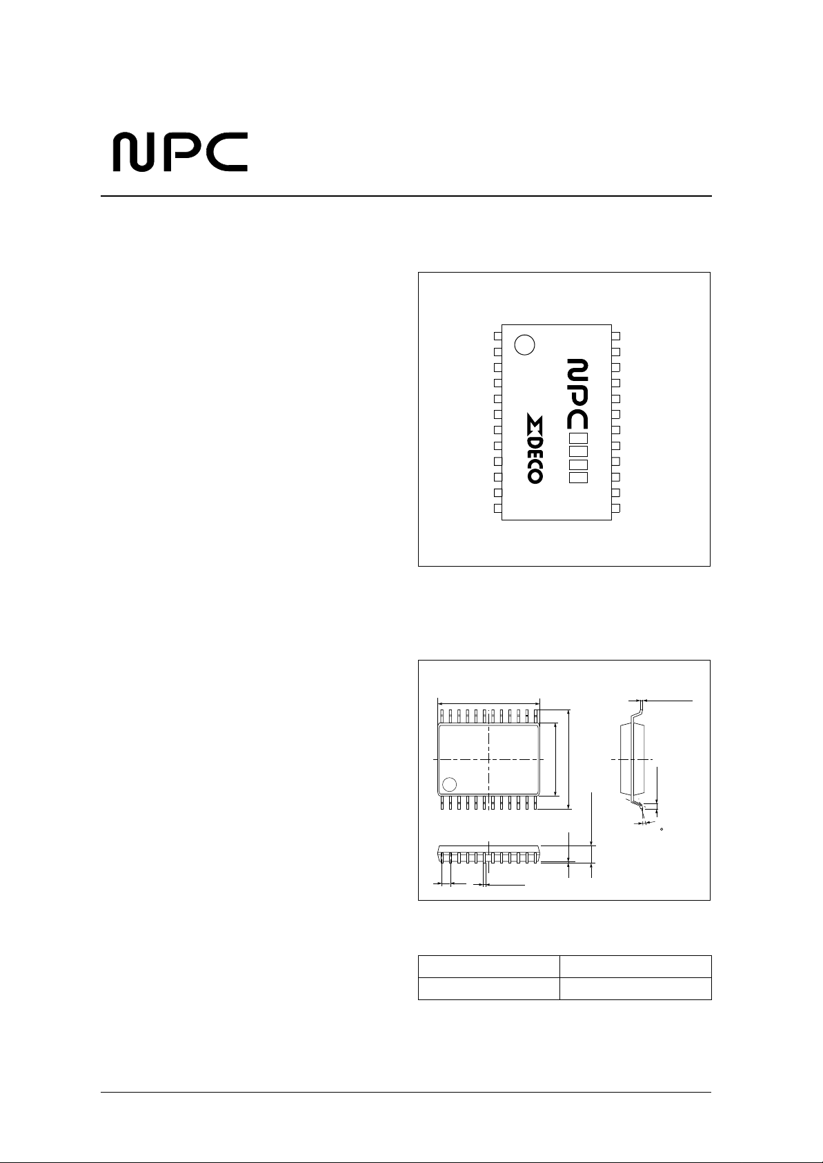
PINOUT
(TOP VIEW)
DVDD
TEST
P / M
AVDDR
RO
AVSSR
TO1
AVSSL
LO
AVDDL
MUTEO
DVSS
1
SM5
879
A
V
12 13
24
PACKAGE DIMENSIONS
Unit: mm
24-pin VSOP
7.8 ± 0.1
5.6 ± 0.1
7.6 ± 0.2
−0.1
+0.2
1.25
0.1 ± 0.1
+0.1
0.22
0.65
−0.05
ORDERING INFOMATION
Device Package
SM5879AV 24pin VSOP
LRCI
BCKI
DI
BB2 / BBON
BB1 / MDT
DEEM / MCK
MUTE / MLEN
XVDD
XTO
XTI
XVSS
CKO
+ 0.05
0.15 − 0.02
0.5 ± 0.2
0 to 10
NIPPON PRECISION CIRCUITS—1
Page 2
−
−
Theoretical Filter Characteristics
Deemphasis OFF overall characteristics
SM5879AV
Parameter
Passband ripple 0 to 0.4535fs 0 to 20.0 kHz
Stopband attenuation 0.5465fs to 7.4535fs 24.1 to 328.7 kHz 32 – –
Built-in analog LPF compensation 0.4535fs 20.0 kHz –
Frequency band Attenuation (dB)
f @ fs = 44.1 kHz min typ max
0.05 – +0.05
0.34 –
Overall frequency characteristic (deemphasis OFF)
0
10
20
30
Gain(dB)
40
50
60
0.0 1.0 2.0 3.0 4.0 5.0 6.0 7.0 8.0
Frequency (Fs)
Passband characteristic (deemphasis OFF)
0.0
0.2
0.4
Gain(dB)
0.6
0.8
0.000 0.125 0.250 0.375 0.500
0.4535
Frequency (Fs)
NIPPON PRECISION CIRCUITS—2
Page 3
−
−
Deemphasis ON overall characteristics
SM5879AV
Parameter
Deviation from ideal deemphasis filter
characteristics
Stopband attenuation 0.5465fs to 7.4535fs 24.1 to 328.7 kHz 36 – –
Built-in analog LPF compensation 0.4535fs 20.0 kHz –
0 to 0.4535fs 0 to 20.0 kHz
Frequency band Attenuation (dB)
f @ fs = 44.1 kHz min typ max
0.09 – +0.23
0.34 –
Overall frequency characteristic (deemphasis ON)
0
10
20
30
Gain(dB)
40
50
60
0.0 1.0 2.0 3.0 4.0 5.0 6.0 7.0 8.0
Frequncy (Fs)
Passband characteristic (deemphasis ON)
0
2
4
6
8
Gain(dB)
10
12
0.000 0.125 0.250 0.375 0.500
0.4535
Frequncy (Fs)
NIPPON PRECISION CIRCUITS—3
Page 4
SM5879AV
PIN DESCRIPTION
Number Name I/O Description
1 DVDD I- Digital supply pin.
2 TEST I Input for testing LSI. Test mode when HIGH.
3 P/M I Parallel/microcontroller setting selection pin. Parallel setting when HIGH.
4 AVDDR - Right-channel analog supply pin.
5 RO O Right channel analog output pin.
6 AVSSR - Right-channel analog ground pin.
7 TO1 O Test mode output. Normally LOW.
8 AVSSL - Left-channel analog ground pin.
9 LO O Left-channel analog output pin.
10 AVDDL O Left-channel analog supply pin.
11 MUTEO O Infinity-zero detection output
12 DVSS - Digital ground pin
13 CKO O Oscillator clock output. 16.9344 MHz.
14 XVSS - Crystal oscillator ground pin
15 XTI I Crystal oscillator or 16.9344-MHz external clock input pin
16 XTO O Crystal oscillator output pin
17 XVDD - Crystal oscillator supply pin
18 MUTE/ MLEN I
19 DEEM/ MCK I
20 BB1/ MDT I
21 BB2/ BBON IO
22 DI I Serial data input pin
23 BCKI I Bit clock input pin
24 LRCI I Sample rate clock (fs) input pin. Left channel when HIGH, and right channel when LOW.
P/M=H; soft mute control pin. Mute is active when HIGH.
P/M=L; microcontroller interface clock
P/M=H; deemphasis control pin. Deemphasis is ON when HIGH.
P/M=L; microcontroller interface clock
P/M=H; bass boost setting switch pin 1
P/M=L; microcontroller interface serial data
P/M=H; bass boost setting switch pin 2
P/M=L; bass boost detection output
NIPPON PRECISION CIRCUITS—4
Page 5
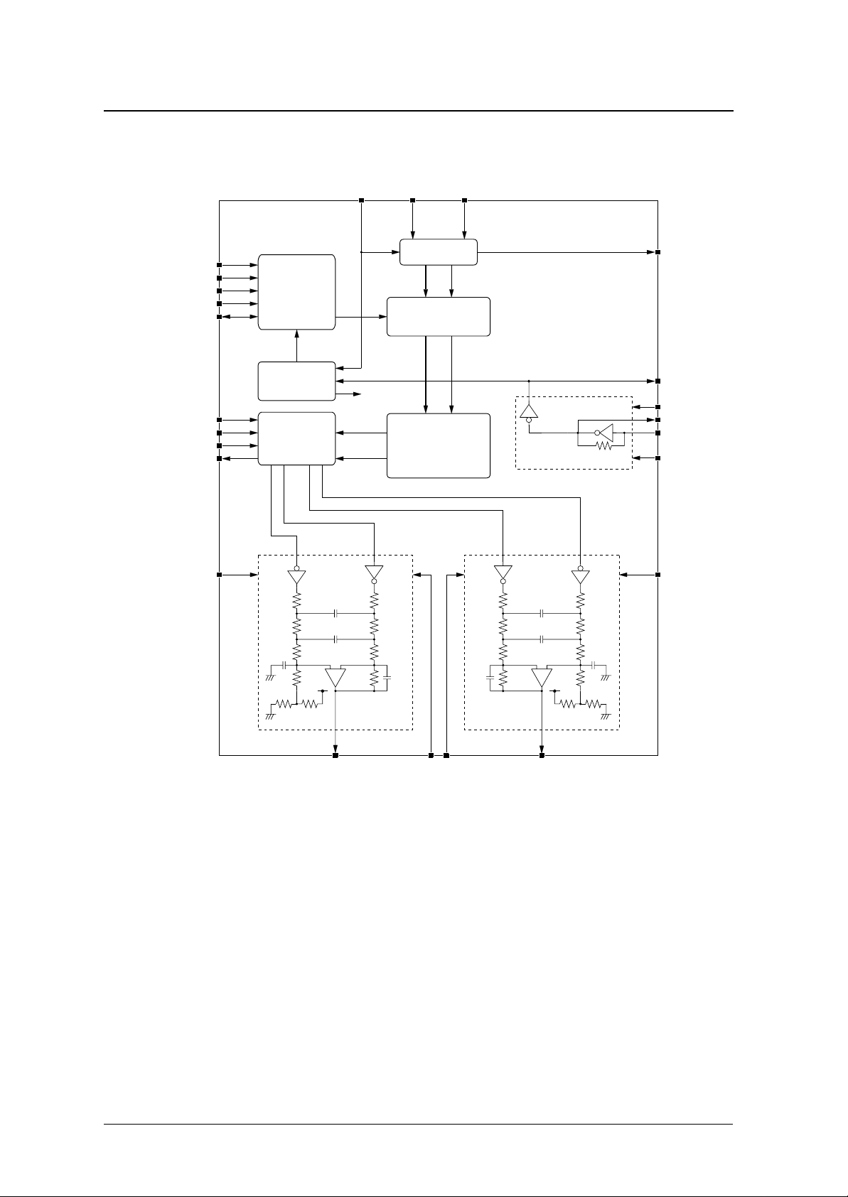
BLOCK DIAGRAM
SM5879AV
LRCI DIBCKI
P /M
MUTE / MLEN
DEEM / MCK
BB1 / MDT
BB2 / BBON
DVSS
DVDD
TEST
TO1
AVDDL
Microcontroller
interface
Timing
control
PWM data
generation block
Filter & attenuation
L
R
Input interface
LR
operation block
LR
Noise shaper
operation block
MUTEO
CKO
XVSS
XTO
XTI
XVDD
AVDDR
+−
LO RO
AVSSRAVSSL
+−
NIPPON PRECISION CIRCUITS—5
Page 6
SM5879AV
SPECIFICATIONS
Absolute Maximum Ratings
DV
= AV
SS
Supply voltage range DV
Input voltage range
XTI input voltage range V
Storage temperature range T
Power dissipation P
Soldering temperature T
Soldering time t
1. Pins TEST, P/ M, MUTE/ MLEN, DEEM/ MCK, BB1/ MDT, BB2/ BBON, DI, BCKI, LRCI
Also applicable during supply switching.
SSL
= AV
SSR
= XV
= 0 V, AV
SS
DD
= AV
DDL
= AV
DDR
Parameter Symbol Rating Unit
, AV
, XV
DD
DD
DD
1
V
IN1
IN
stg
D
sld
sld
−
−
+
−
+
−
°
°
−
−
−
−
−
−
−
°
0.3 to 7.0 V
DV
XV
SS
SS
0.3 to DV
0.3 to XV
55 to 125
0.3 V
DD
0.3 V
DD
C
250 mW
255
C
10 s
Recommended Operating Conditions
DV
= AV
SS
Supply voltage range DV
Supply voltage variation
Operating temperature range T
note) Since DVDD, XVDD, AVDDL, and AVDDR are connected via the LSI base board, current may flow if potential difference occurs among them.
SSL
= AV
SSR
= XV
= 0 V, AV
SS
DD
= AV
DDL
= AV
DDR
Parameter Symbol Rating Unit
, AV
DV
DV
XV
DV
DV
XV
, XV
DD
DD
DD
XV
DD
DD
DD
SS
SS
,
DD
AV
,
DD
AV
,
DD
XV
,
SS
AV
,
SS
AV
SS
SS
opr
2.7 to 3.3 V
±0.1 V
20 to 70
C
NIPPON PRECISION CIRCUITS—6
Page 7

DC Electrical Characteristics
SM5879AV
Parameter Symbol Condition
DVDD digital supply current
XVDD system clock supply current
AVDD analog supply current
XTI HIGH-level input voltage V
XTI LOW-level input voltage V
XTI AC-coupled input voltage V
HIGH-level input voltage
LOW-level input voltage
HIGH-level output voltage
LOW-level output voltage
XTI HIGH-level input current I
XTI LOW-level input current I
Input leakage current
1. DV
= AV
DD
2. I
DDA
3. Pins TEST, P/ M, MUTE/ MLEN, DEEM/ MCK, BB1/ MDT, BB2/ BBON, DI, BCKI, LRCI
= XV
DD
is the total current.
1
1
1
3
3
4
4
3
= 2.7V, XTI clock input frequency f
DD
I
I
I
V
V
DDD
DDX
DDA
INAC
V
V
IH1
IL1
I
ILH
I
IH1
IL1
IH2
IL2
OH
OL
LL
2
Clock input 0.7XV
Clock input – – 0.3XV
IOH = −0.5mA DVDD − 0.4 – – V
IOL = 0.5mA – – 0.4 V
VIN = XV
DD
VIN = 0 V – 4 10 µA
VIN = DV
DD
VIN = 0V -1.0 – 1.0 µA
= 16.9344 MHz, no output load.
XTI
4. Pins MUTEO, CKO, BB2/ BBON, TO1
Rating
min typ max
– 3.70 7.40 mA
– 0.55 1.10 mA
– 0.68 1.36 mA
DD
0.3XV
DD
0.7DV
DD
– – 0.3DV
––V
DD
––V
––V
DD
– 4 10 µA
-1.0 – 1.0 µA
Unit
V
p-p
V
NIPPON PRECISION CIRCUITS—7
Page 8

AC Electrical Characteristics
System clock (XTI)
Crystal Oscillator
SM5879AV
Parameter Symbol
Oscillator frequency f
External clock input
Parameter Symbol
HIGH-level clock pulsewidth t
LOW-level clock pulsewidth t
Clock pulse cycle t
XTI input clock
t
CWL
Serial input (BCKI, DI, LRCI)
OSC
CWH
CWL
XI
t
Rating
Unit
min typ max
10.0 16.9344 18.5 MHz
Rating
Unit
min typ max
20.0 29.5 50 ns
20.0 29.5 50 ns
54.0 59.0 100 ns
XI
V
IH1
0.5V
DD
V
t
CWH
IL1
Parameter Symbol
BCKI HIGH-level pulsewidth t
BCKI LOW-level pulsewidth t
BCKI pulse cycle t
DI setup time t
DI hold time t
Last BCKI rising edge to LRCI edge t
LRCI edge to first BCKI rising edge t
Serial input timing
BCKI
LRCI
t
BCWH
DI
t
BCWL
t
BCY
t
DS
t
LB
t
DH
BCWH
BCWL
BCY
DS
DH
BL
LB
Rating
min typ max
50 – – ns
50 – – ns
6t
XI
––ns
50 – – ns
50 – – ns
50 – – ns
50 – – ns
0.5VDD
0.5VDD
0.5VDD
t
BL
Unit
NIPPON PRECISION CIRCUITS—8
Page 9

Control input
P/M=H
SM5879AV
Parameter Symbol
Rise time t
Fall time t
t r
MUTE
DEEN
BB1
BB2
P/M=L
Parameter Symbol
MCK LOW-level pulsewidth t
MCK HIGH-level pulsewidth t
MCK pulse width t
MDT setup time t
MDT hold time t
MLEN setup time t
MLEN hold time t
Rise time t
Fall time t
90%
10%
Figure 1.
r
f
MCWL
MCWH
Mcy
MDS
MDH
MLH
MLW
r
f
Rating
min typ max
– – 50 ns
– – 50 ns
t r
90%
10%
min typ max
200 – – ns
200 – – ns
400 – – ns
100 – – ns
100 – – ns
100 – – ns
200 – – ns
– – 50 ns
– – 50 ns
0.5VDD
Rating
Unit
Unit
MCK
MDT
MLEN
t MCWH
0.5VDD
t MCWL
t MCY
0.5VDD
t MDS t MDH
0.5VDD
t MLS t MLH
t MLW
NIPPON PRECISION CIRCUITS—9
Page 10

AC Analog Characteristics
SM5879AV
DVSS = AV
DEEM=0V, BB1=2.7V, BB2=2.7V, crystal oscillator frequency f
Total harmonic distortion THD + N 1 kHz, 0 dB – 0.0075 0.015 %
LSI output level V
Evaluation board output level V
Dynamic range D.R 1 kHz, −60 dB 86.0 91.0 – dB
Signal-to-noise ratio
Channel separation Ch. Sep 1 kHz, −∞/0 dB 80.0 87.0 – dB
1. Signal-to-noise is measured following a device reset, with DA TA = 0 (DI = LOW). Under these conditions, the signal-to-noise ratio includes noise-shaper
noise.
= AV
SSL
Parameter Symbol Condition
1
= XVSS = 0 V, DVDD = AV
SSR
out1
out2
S/N 1 kHz, 0/−∞ dB 86.0 91.5 – dB
DDL
1 kHz, 0 dB 0.65 0.70 0.75 V
1 kHz, 0 dB – 0.70 – V
= AV
= XVDD = 2.7V, P/M=2.7V, MUTE=0V,
DDR
= 16.9344 MHz, Ta = 25 °C
OSC
Rating
min typ max
Unit
rms
rms
AC Measurement Circuit and Conditions
Measurement circuit block diagram
Signal
Generator
CKO(384fs)
BCK
LRCK(fs)
DATA
Evaluation
Board
Left Channel
Right Channel
L/R Channel
Selector
Distortion
Analyzer
fs= 44.1kHz
DATA= 16bit
10kΩ Input Impedance
NF Corporation 3346A
Measurement conditions
Parameter
Total harmonic distortion THD + N
Output level V
Dynamic range DR D-RANGE
Signal-to-noise ratio S/N THRU
Channel separation Ch. Sep THRU
1. Pins LO and RO should have an output load of 10 kΩ (min).
1
Symbol
out
3346A left/right-channel selector
switch
THRU
RMS Measurement
Shibasoku AD725C
AD725C distortion analyzer with
built-in filter
20 kHz lowpass filter ON
400 Hz highpass filter OFF
20 kHz lowpass filter ON
400 Hz highpass filter OFF
JIS A filter ON
20 kHz lowpass filter ON
400 Hz highpass filter OFF
NIPPON PRECISION CIRCUITS—10
Page 11

Measurement circuit
SM5879AV
5.6k
100p
220p
33k
22k
L OUT
100p
100
100k
+-
2.2u
0.1u
-
+
NJM
2100D
6
33u
5
22k
-
+
8
33u
VCC
+
-
470u
5.6k
VEE
220p
22k
R OUT
100p
100
+-
2.2u
0.1u
-
+
NJM
26
2100D
33u
3
22k
-
+
8
33u
6.8k
5.6k 6.8k
1500p
5.6k
1500p
1
4
NJM
--
++
2100D
2
3
22k
-
22k
33k
+
33u
100p
33k
22k
4
NJM
--
++
2100D
5
22k
-
+
33k
33u
100k
BBON
-+
-+
33u 33u
16.9344MHz
10p
10p
0.01u
CKO
XVSS
XTI
XTO
XVDD
MUTE/MLEN
DEEM/MCK
BB1/MDT
BB2/BBON
DI
BCKI
LRCI
SM5879
CKO
MUTEO
MDT
MCK
DVSS
MUTEO
AVDDL
AVSSL
AVSSR
AVDDR
TEST
DVDD
LRCI
TO1
P/M
BCKI
-+
-+
33u 33u
LO
-+
100u
0.01u
0.01u
0.01u
100u
DVDD AVDDDVSS AVSS TO1
-+
RO
DI
MLEN
NIPPON PRECISION CIRCUITS—11
Page 12

FUNCTIONAL DESCRIPTION
System Clock
SM5879AV
Note that the input clock accuracy and jitter greatly
influence the AC analog characteristics.
The system clock can be controlled by a crystal oscillator consisting of a crystal connected between XTI
and XTO and a built-in CMOS invertor or, alterna-
System Reset (RSTN)
System reset for SM5879AV is performed by a builtin power ON reset circuit.
At system reset, the internal arithmetic operation and
output timing counter are synchronized with the next
LCRI rising edge and thereby reset again for synchronization with external elements.
Power on Switch
123 910
LRCI
Internal
Reset
LO
RO
tively, an external system clock. Since the built-in
CMOS invertor has a feedback resistor, the external
system clock can be AC coupled to XTI. The system
clock is output from CKO.
Analog output is muted by this resetting, and muting
is cleared by the ninth LCRI rise (See Figure 1).
However, noise is generated due to the change in
PWM output during a timing reset. An external mute
circuit is necessary to prevent this noise.
Output Muted
Figure 2. System reset timing
Audio Data Input (DI, BCKI, LRCI)
The digital audio data is input on DI in MSB-first, 2scomplement, 16-bit serial format.
Serial data bits are read into the SIPO register (serialto-parallel converter re gister) on the rising edge of the
bit clock BCKI.
LRCI
BCKI
(MAX64fs)
DI
16bit
MSB LSB
Figure 3.
The bit clock frequency on BCKI should be between
32fs and 64fs.
1 / fs
RchLch
MSB LSB
16bit
NIPPON PRECISION CIRCUITS—12
Page 13

Selection and Setting of Functions
SM5879AV
SM5879AV offers a variety of functions. Fundamentally, there are two methods available for selecting
and setting these functions.
One method is using an external input pin; this is
called parallel setting. The other method is by using
the microcontroller interface, which is called microcontroller setting.
Microcontroller interface refers here to serial data
transfer from the microcontroller using the three pins
MDT, MCK, and MLEN.
These two methods of setting and selection are set by
the P/M pin.
When P/M is HIGH, parallel setting is used.
When P/M is LOW, microcontroller setting is used.
Table 1. Selection and Setting of Functions
Function Setting Methods
Function
Bass boost BB1, BB2 FBB1, FBB2 Bass boost
Bass boost detection output None Output to BBON Bass boost detection output
Deemphasis filter DEEM FDEM Deemphasis filter
Soft mute MUTE
Attenuator setting None 7 bits (A6 - A0) Attenuation
Monaural setting None MONO, CSEL Stereo/mono output setting
Parallel setting
Related external pin name
(When P/M is HIGH)
Microcontroller setting
Related flag
(When P/M is LOW)
None
(Enabled by attenuator)
Notes
Soft mute
NIPPON PRECISION CIRCUITS—13
Page 14

Microcontroller Interface
SM5879AV
For microcontroller setting (when P/M is HIGH), the
microcontroller interface consisting of MDT (data),
MCK (clock) and MLEN (latch enable) can be used.
Data from the microcontroller is input to the inputstage shift registers at the rise of MCK. Changes in
MDT should be performed at the rise of MCK.
MLEN
MCK
MDT
D0
D1 D2 D3 D4 D5 D6 D7
Figure 4. Format of microcontroller interface input
Table 2. microcontroller setting flags
Microcontroller
serial data
D7 0 1
Flag
Serial data in the shift registers is latched in parallel
to the flag registers at the rise of MLEN.
Two flag registers are available, divided into the
attenuation factor and mode flag by the D7 data.
D6 A6 D5 A5 FDEM
D4 A4 FBB1
D3 A3 FBB2
D2 A2 MONO
D1 A1 CSEL
D0 A0 -
A0 to A6: Attenuation factor (A6: MSB)
FDEM: Deemphasis ON/OFF (ON when 1)
FBB1: Bass boost setting switch flag 1
FBB2: Bass boost setting switch flag 2
MONO: Stereo/mono setting (Mono when 1)
CSEL: Mono output channel selection
(Right channel when 1)
NIPPON PRECISION CIRCUITS—14
Page 15

SM5879AV
Bass Boost
T w o types of bass boost and gain modification can be
set by either parallel or microcontroller.
Table 3.
Parallel setting
pin name
Microcontroller
setting flag
BB1 BB2
Mode
FBB1 FBB2
H H Flat 1
H L Bass boost MIN
L H Bass boost MAX
L L Flat2
3
Max. Chrasteristic
2
1
Flat1 (0dB)
0
-1
Min. Charasteristic
-2
-3
Boost (dB)
-4
-5
-6
-7
Flat2 (-8dB)
-8
-9
10 100 1000 10
Frequency (Fs)
4
10
5
Figure 5. Bass boost mode frequency response
Bass boost detection output
With microcontroller setting (when P/M is LOW),
the 21st pin is the BBON output pin and functions as
output that detects the bass boost mode.
Table 4.
Microcontroller
setting flag
BB1 BB2 Mode BBON pin
H H Flat 1 L
H L Bass boost MIN H
L H Bass boost MAX H
L L Flat 2 H
BBON output is LOW when the bass boost mode is
set to Flat 1 and HIGH in all other cases.
NIPPON PRECISION CIRCUITS—15
Page 16

SM5879AV
Deemphasis filter
The built-in deemphasis filter in the SM5879AV
operates at fs = 44.1 kHz.
Table 5.
Parallel setting pin name DEEM
Microcontroller setting
flag
FDEM
HON
L OFF
Soft Mute
Deemphasis mode
With parallel setting (when P/M is HIGH), soft mute
can be activated by the MUTE pin level setting using
the built-in attenuation counter. When muting is activated, MUTE is HIGH.
MUTE
0dB
(Gain)
−∞
1024/fs
Figure 6. Example of soft mute operation
When soft mute is activated, the attenuation counter
operates and lowers gain in 128 steps.
The time until mute is activated is approximately
1024/fs ≈ 23.2 msec. The time required to release
muting is the same.
1024/fs
NIPPON PRECISION CIRCUITS—16
Page 17

SM5879AV
Attenuation
The SM5879AV loads the attenuation factor with
serial data by means of the microcontroller interface,
thus enabling attenuation operation.
MLEN
MCK
MDT
A0 A1
(LSB) (MSB)
D0
A2
D1 D2 D3 D4 D5 D6 D7
Figure 7. Method of setting the attenuation factor
The attenuation computation is performed by multiplying the output of the internal 7-bit UP/DOWN
counter output data by the signal data. When the con-
L channel
Gain 20
log
127
[dB]
DATT
--------------- -
×
=
R channel
DATT
--------------- -
Gain 20
×
log
127
[dB] =
When DATT = 0, this becomes -∞.
When the attenuation factor is changed, it is
smoothly changed from the previous setting until it
reaches the value of the new setting as expressed by
the above equations. The time required to change
Setting1
(Gain)
Setting2
A3 A4 A5 A6 0
tents of the counter are DATT, gain can be expressed
by the following equations.
gain is approximately 1024 fs ≈ 23.2 msec when the
time required to change one step of the attenuation
factor is approximately 8 / fs ≈ 181.4 µsec over the
range 0 dB to -∞.
Setting5
Setting3
Setting4
Time
Figure 8. Example of attenuation gain
NIPPON PRECISION CIRCUITS—17
Page 18

SM5879AV
Stereo/Mono Output Setting
Mono output can be set via the microcontroller
(when P/M is HIGH).
Table 6.
Microcontroller
setting flag
MONO CSEL Output
H H R channel
H L L channel
LH
LL
Infinity-Zero Detection Output
HIGH level is output from the infinity-zero detection
output pin in the following cases with the
SM5879AV.
×
LRCI
RSTN
MUTEO
Internal
Status
DI
1 2 3 9
Signal
Initialize
Figure 9.
Stereo
(1) From the time that power ON is reset until the
first data comes in.
(2) When the LOW level space of the DI pin has continued for 2
14
(1/fs) ≈ 0.37 [sec] or more.
14
2 /fs
SignalNo Signal
NIPPON PRECISION CIRCUITS—18
Page 19

TIMING DIAGRAMS
Input Timing (DI, BCKI, LRCI)
LRCI
BCKI
(MAX64fs)
DI
TYPICAL APPLICATIONS
Input Interface Circuits
Normal Speed
SM5879AV
1 / fs
MSB LSB
16bit
RchLch
MSB LSB
X'tal (16.9344MHz)
16bit
SONY
CXD2500
PSSL
XTAI
LRCK
DA16
DA15
16.9344MHz
44.1kHz
2.1168MHz
XTI XTO
CKO
LRCI
DI
BCKI
SM5879
NIPPON PRECISION CIRCUITS—19
Page 20

SM5879AV
NIPPON PRECISION CIRCUITS INC. reserves the right to make changes to the products described in this data sheet in order to
improve the design or performance and to supply the best possible products. Nippon Precision Circuits Inc. assumes no responsibility for
the use of any circuits shown in this data sheet, conveys no license under any patent or other rights, and makes no claim that the circuits
are free from patent infringement. Applications for any devices shown in this data sheet are for illustration only and Nippon Precision
Circuits Inc. makes no claim or warranty that such applications will be suitable for the use specified without further testing or modification.
The products described in this data sheet are not intended to use for the apparatus which influence human lives due to the failure or
malfunction of the products. Customers are requested to comply with applicable laws and regulations in effect now and hereinafter,
including compliance with export controls on the distribution or dissemination of the products. Customers shall not export, directly or
indirectly, any products without first obtaining required licenses and approvals from appropriate government agencies.
NIPPON PRECISION CIRCUITS INC.
NIPPON PRECISION CIRCUITS INC.
4-3, Fukuzumi 2 chome
Koto-ku, Tokyo 135-8430, Japan
Telephone: 03-3642-6661
Facsimile: 03-3642-6698
NC9702BE 1997.11
NIPPON PRECISION CIRCUITS—20
 Loading...