

Page 1
SM5878AM/AV
NIPPON PRECISION CIRCUITS INC.
OVERVIEW
The SM5878AM/AV is a 3rd-order Σ∆ , 2-channel
D/A converter LSI for digital audio reproduction
equipment. It also incorporates an 8-times
oversampling digital filter and analog, post-con verter
lowpass filters.
The SM5878AM/AV has digital deemphasis filter,
attenuator, and soft mute circuits built-in. Doublespeed operation and low-voltage operation are also
supported.
SM5878AM/AV D/A converter incorporates 3rdorder ∑∆ modulator and DEM (Dynamic Element
Mating) circuits for high performance, even in the
presence of clock jitter.
The SM5878AM/AV operates from a 4.5 to 5.5 V
supply, and is available in 24-pin SSOP or VSOPs.
3rd-order Σ∆ , 2-channel D/A converter
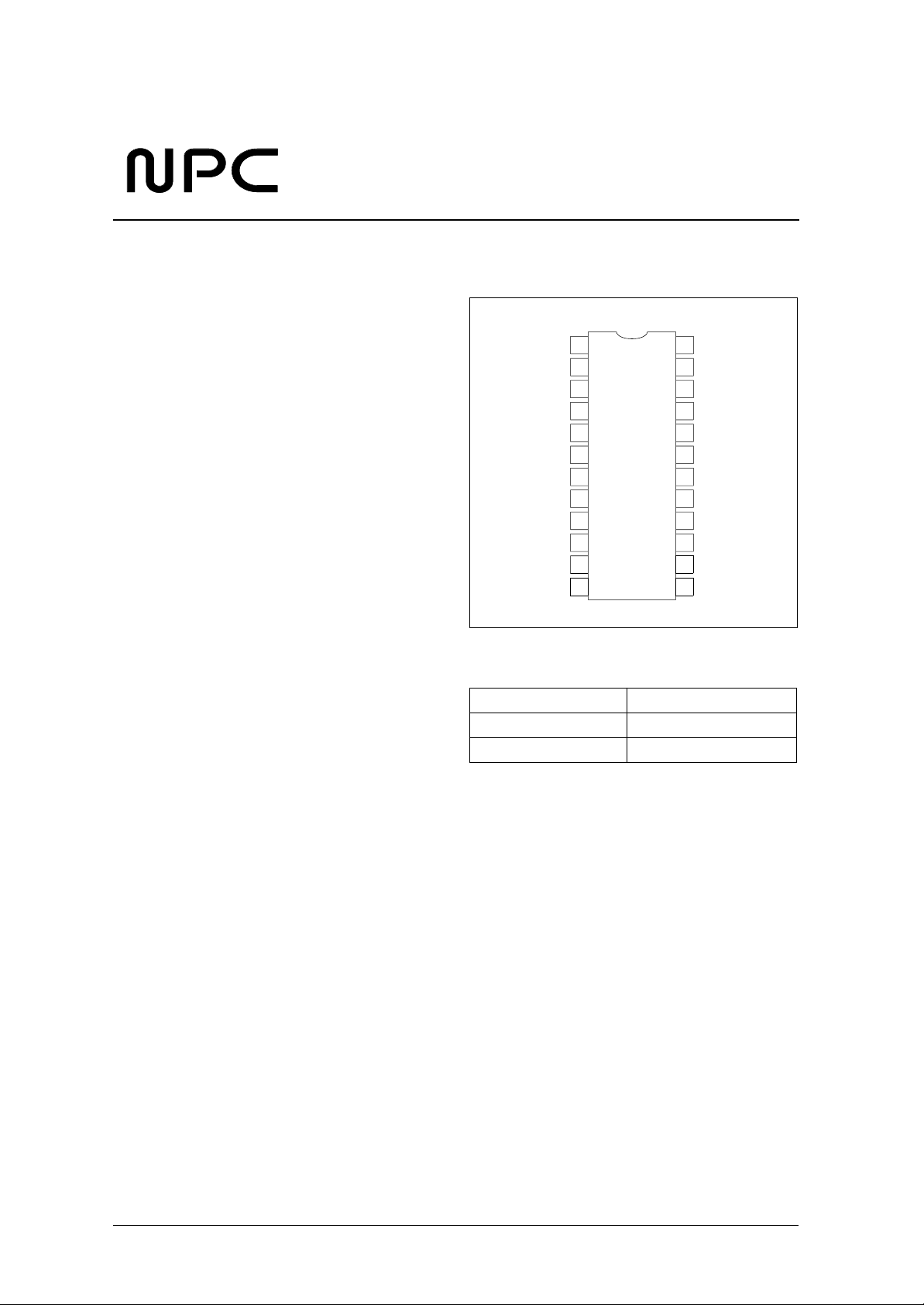
PINOUT
1MUTE
2DEEM
3CKO
4DVSS
5BCKI
6DI
7DVDD
8LRCI
9TSTN
10TO1
11AVDDL
12LO 13 AVSS
SM5878
24 ATCK
23 MODE
22 RSTN
21 DS
20 XVSS
19 XTO
18 XTI
17 XVDD
16 MUTEO
15 AVDDR
14 RO
FEATURES
4.5 to 5.5 V operating supply voltage range
■
44.1 kHz sampling frequency
■
Normal (384fs) and double-speed (192fs),
■
16.9344 MHz system clock
16.9344 MHz crystal oscillator circuits built-in
■
16-bit, MSB first, rear-packed serial data input
■
format ( ≤ 64fs bit clock)
8-times oversampling digital filter
■
• 32 dB stopband attenuation
• ±0.05 dB passband ripple
Deemphasis filter operation
■
• 36 dB stopband attenuation
• − 0.09 to +0.23 dB deviation from ideal
deemphasis filter characteristics
Attenuator
■
• 6-bit attenuator (64 steps)
• Soft mute function when MODE is HIGH
(approx. 1024/fs total muting time)
Built-in infinity-zero detector
■
Σ∆ 2-channel D/A converter
■
• 3rd-order noise shaper
• 32fs oversampling (16fs for double-speed
mode)
2nd-order analog, post-converter lowpass filters
■
built-in
24-pin SSOP/VSOP
■
Molybdenum-gate CMOS process
■
ORDERING INFORMATIONS
DEVICE PACKAGE
SM5878AM 24 - pin SSOP
SM5878AV 24 - pin VSOP
NIPPON PRECISION CIRCUITS—1
Page 2
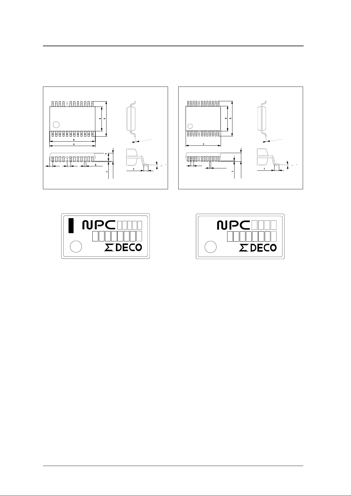
PACKAGE DIMENSIONS
Unit: mm
SM5878AM/AV
24-pin SSOP
10.05 0.20
10.20 0.30
0.7 0.8
0.36 0.10
Package Marking
7.80 0.30
5.40 0.20
1.80 0.10
0.10 0.10
2.10MAX
0.50 0.20
24-pin VSOP
7.6 0.2
5.6 0.1
0.05
0.5 0.2
0.15
+
− 0.02
010
0.15
0.1
+
0.05
−
010
7.8 0.1
0.65
0.22
+0.1
−0.05
+0.2
0.1 0.1
−0.1
1.25
Package Marking
MA8785MS
VA8785MS
NIPPON PRECISION CIRCUITS—2
Page 3
BLOCK DIAGRAM
SM5878AM/AV
LRCI DIBCKI
MODE
ATCK
MUTE
RSTN
DS
DVSS
DVDD
TSTN
TO1
AVDDL
Attenuation
counter
Timing
control
11Level
DEM DAC
11Level
DEM DAC
Input interface
LR
Filter & attenuation
operation block
LR
Noise shaper
operation block
11Level
DEM DAC
11Level
DEM DAC
MUTEO
DEEM
CKO
XVSS
XTO
XTI
XVDD
AVDDR
+−
LO AVSS RO
+−
PIN DESCRIPTION
Number Name I/O Description
1 MUTE Ip
2 DEEM Ip Deemphasis control. Deemphasis is ON when HIGH, and OFF when LOW.
3 CKO O 16.9344 MHz clock output
4 DVSS - Digital ground
5 BCKI Ip Bit clock input
6 DI Ip Serial data input
7 DVDD - Digital supply
8 LRCI Ip
9 TSTN Ip Test pin. Test mode when LOW.
When MODE is HIGH: Soft mute ON/OFF control. Mute is active when HIGH.
When MODE is LOW: Attenuator level direction control. The attenuator direction is down when HIGH.
Input sample data rate (fs) clock input pin. Left-channel input when HIGH, and right-channel input when
LOW .
NIPPON PRECISION CIRCUITS—3
Page 4
−
−
+
−
+
−
°
°
−
−
−
−
−
SM5878AM/AV
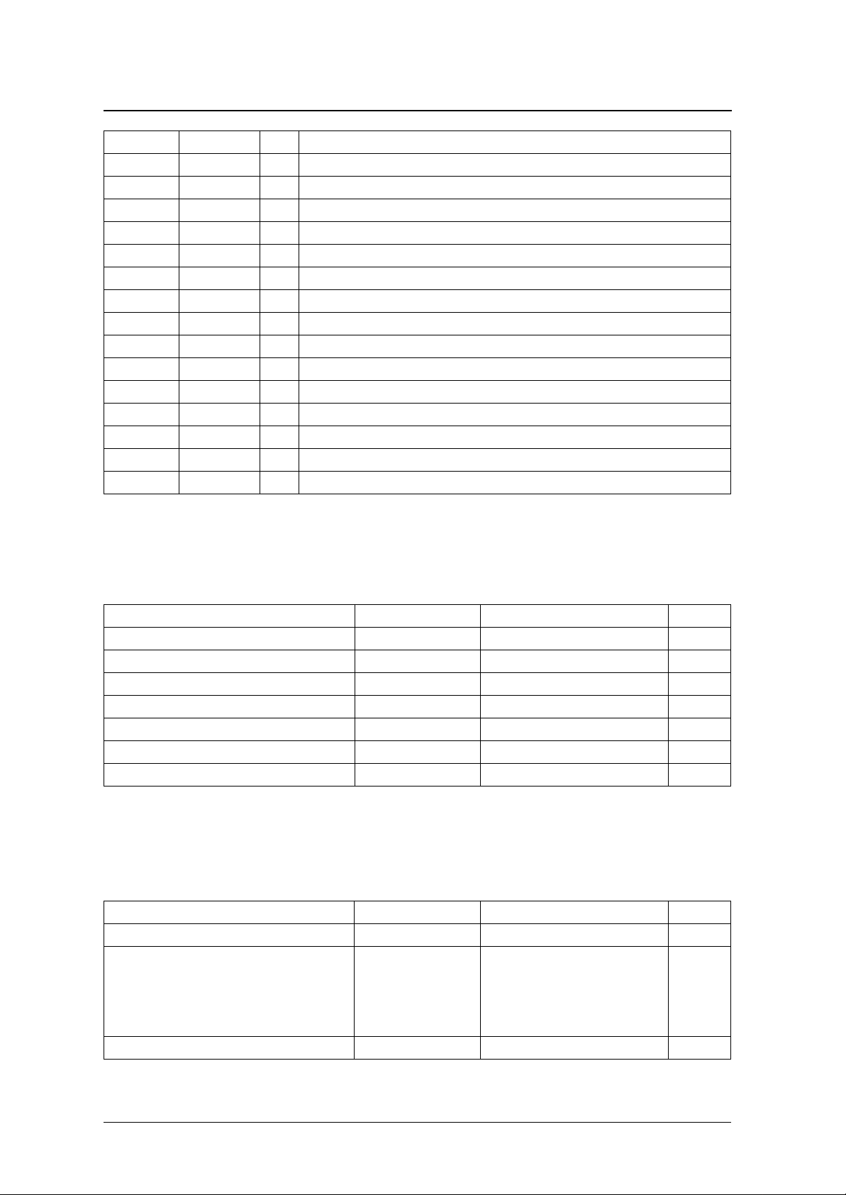
Number Name I/O Description
10 TO1 O Test output 1. Normally LOW.
11 AVDDL - Left-channel analog supply
12 LO O Left-channel analog output
13 AVSS - Analog ground
14 RO O Right-channel analog output
15 AVDDR - Right-channel analog supply
16 MUTEO O Infinity-zero detection output
17 XVDD - Crystal oscillator supply
18 XTI I Crystal oscillator or 16.9344 MHz external clock input
19 XTO O Crystal oscillator output
20 XVSS - Crystal oscillator ground
21 DS Ip Double/Normal-speed mode select. Double-speed mode when HIGH.
22 RSTN Ip Reset pin. Reset when LOW.
23 MODE Ip Soft mute/attenuator mode select. Soft mute mode when HIGH.
24 ATCK Ip Attenuator level setting clock. Disabled when MODE is HIGH.
−
−
° C
SPECIFICATIONS
Absolute Maximum Ratings
DV
= AV
SS
Supply voltage range DV
Input voltage range
XTI input voltage range V
Storage temperature range T
Power dissipation P
Soldering temperature T
Soldering time t
1. Pins MUTE, DEEM, BCKI, DI, LRCI, TSTN, DS, RSTN, MODE and ATCK.
Also applicable during supply switching.
Recommended Operating Conditions
DV
= AV
SS
Supply voltage range DV
Supply voltage variation
Operating temperature range T
SS
= XV
= 0 V, AV
SS
DD
= AV
DDL
= AV
DDR
Parameter Symbol Rating Unit
, AV
DD
1
SS
= XV
= 0 V, AV
SS
DD
= AV
DDL
= AV
DDR
Parameter Symbol Rating Unit
, AV
DD
DV
DD
DV
DD
XV
DD
DV
SS
DV
SS
XV
SS
, XV
DD
DD
V
IN1
IN
stg
D
sld
sld
, XV
DD
DD
XV
,
DD
AV
,
DD
AV
,
DD
XV
,
SS
AV
,
SS
AV
SS
opr
0.3 to 7.0 V
DV
XV
SS
SS
0.3 to DV
0.3 to XV
0.3 V
DD
0.3 V
DD
55 to 125
250 mW
255
10 s
4.5 to 5.5 V
±0.1 V
40 to 85
C
C
note) Since DVDD, XVDD, AVDDL, and AVDDR are connected via the LSI substrate, current may flow if potential difference occurs among them.
NIPPON PRECISION CIRCUITS—4
Page 5
DC Electrical Characteristics
DV
= AV
SS
C
SS
= XV
= 0 V, DV
SS
DD
= AV
DD
= XV
SM5878AM/AV
= 4.5 to 5.5 V, AV
DD
DD
= AV
DDL
= AV
°
−
, T
DDR
= − 40 to 85
a
Parameter Symbol Condition
DVDD digital supply current
XVDD system clock supply current
AVDD analog supply current
XTI HIGH-level input voltage V
XTI LOW-level input voltage V
XTI AC-coupled input voltage V
HIGH-level input voltage
LOW-level input voltage
HIGH-level output voltage
LOW-level output voltage
CKO HIGH-level output voltage V
CKO LOW-level output voltage V
XTI HIGH-level input current I
XTI LOW-level input current I
LOW-level input current
Input leakage current
1. DV
= AV
DD
2. I
DDA
3. Pins MUTE, DEEM, BCKI, DI, LRCI, TSTN, DS, RSTN, MODE and ATCK.
= XV
DD
is the total current.
1
1
1
3
3
4
4
4
4
= 5 V, DS = 5 V (double speed), XTI clock input frequency f
DD
I
V
V
I
DDD
I
DDX
DDA
INAC
V
V
OHA
OHC
I
I
IH1
IL1
IH2
IL2
OLA
OLC
IH1
IL1
IL2
LH
2
Clock input 0.7XV
Clock input – – 0.3XV
I
= − 1 mA AV
OH
I
= 1 mA – – 0.4 V
OL
IOH = −1 mA DVDD − 0.4 – – V
IOL = 1 mA – – 0.4 V
VIN = XV
DD
VIN = 0 V – 9 18 µA
VIN = 0 V – 9 18 µA
VIN = DV
DD
4. Pins TO1 and MUTEO.
min typ max
–1015mA
– 1.5 3 mA
– 8.5 12 mA
DD
0.3XV
DD
2.4 – – V
– – 0.5 V
0.4 – – V
DD
– 9 18 µA
– – 1.0 µA
= 16.9344 MHz, no output load.
XTI
Rating
Unit
––V
DD
––V
V
p-p
AC Electrical Characteristics
System clock (XTI)
Crystal Oscillator
Parameter Symbol
Oscillator frequency f
OSC
Rating
Unit
min typ max
4.0 16.9344 20.0 MHz
NIPPON PRECISION CIRCUITS—5
Page 6

External clock input
SM5878AM/AV
Parameter Symbol
HIGH-level clock pulsewidth t
LOW-level clock pulsewidth t
Clock pulse cycle t
XTI input clock
t
CWH
t
XI
Serial input (BCKI, DI, LRCI)
Parameter Symbol
BCKI HIGH-level pulsewidth t
BCKI LOW-level pulsewidth t
BCKI pulse cycle t
DI setup time t
DI hold time t
Last BCKI rising edge to LRCI edge t
LRCI edge to first BCKI rising edge t
CWH
CWL
XI
BCWH
BCWL
BCY
DS
DH
BL
LB
t
CWL
Rating
Unit
min typ max
20.0 29.5 125 ns
20.0 29.5 125 ns
50.0 59.0 250 ns
Rating
Unit
min typ max
50 – – ns
50 – – ns
6t
XI
––ns
50 – – ns
50 – – ns
50 – – ns
50 – – ns
0.5V
V
IH1
DD
V
IL1
Serial input timing
BCKI
DI
LRCI
t
BCWH
1.5V
t
BCWL
t
BCY
1.5V
t
DS
t
DH
1.5V
t
LB
t
BL
NIPPON PRECISION CIRCUITS—6
Page 7

SM5878AM/AV
Control input (MUTE, MODE, ATCK, DEEM, DS)
Parameter Symbol
ATCK LOW-level pulsewidth t
ATCK HIGH-level pulsewidth t
MUTE setup time t
MUTE hold time t
MODE setup time t
MODE hold time t
Rise time t
Fall time t
1. fs is LRCI clock frequency.
Control input timing
MUTE
MODE
t
t
MUS
MOS
t
t
MUH
MOH
ATWL
ATWH
MUS
MUH
MOS
MOH
r
f
Rating
min typ max
1
0.5/fs
0.5/fs
1
––µs
––µs
100 – – ns
100 – – ns
100 – – ns
100 – – ns
– – 50 ns
– – 50 ns
Unit
1.5 V
ATCK
DEEM
DS
MUTE
MODE
ATCK
t
ATWL
t
2.4 V
0.5 V
Reset Input (RSTN)
Parameter Symbol
RSTN LOW-level pulsewidth after supply rising edge t
ATWH
1.5 V
t
f
t
r
0.5 V
2.4 V
1.5 V
Rating
Unit
min typ max
RSTN
50 – – ns
NIPPON PRECISION CIRCUITS—7
Page 8

Theoretical Filter Characteristics
Deemphasis OFF overall characteristics
SM5878AM/AV
Parameter
Frequency band Attenuation (dB)
f @ fs = 44.1 kHz min typ max
Passband ripple 0 to 0.4535fs 0 to 20.0 kHz −0.05 – +0.05
Stopband attenuation 0.5465fs to 7.4535fs 24.1 to 328.7 kHz 32 – –
Built-in analog LPF compensation 0.4535fs 20.0 kHz – −0.34 –
Overall frequency characteristic (deemphasis OFF)
0
10
20
30
Gain (dB)
40
50
60
0.0
Passband characteristic (deemphasis OFF)
0.0
0.2
0.4
Gain (dB)
0.6
0.8
Frequency (fs)
Frequency (fs)
8.07.06.05.04.03.02.01.0
0.5000.3750.2500.125 0.45350.000
NIPPON PRECISION CIRCUITS—8
Page 9

Deemphasis ON overall characteristics
SM5878AM/AV
Parameter
Frequency band Attenuation (dB)
f @ fs = 44.1 kHz min typ max
Deviation from ideal deemphasis filter
characteristics
0 to 0.4535fs 0 to 20.0 kHz −0.09 – +0.23
Stopband attenuation 0.5465fs to 7.4535fs 24.1 to 328.7 kHz 36 – –
Built-in analog LPF compensation 0.4535fs 20.0 kHz – −0.34 –
Overall frequency characteristic (deemphasis ON)
0
10
20
30
Gain (dB)
40
50
60
0.0
Passband characteristic (deemphasis ON)
0
2
4
6
Gain (dB)
8
10
12
0.000
Frequency (fs)
Frequency (fs)
8.07.06.05.04.03.02.01.0
0.5000.3750.2500.125 0.4535
NIPPON PRECISION CIRCUITS—9
Page 10

AC Analog Characteristics
SM5878AM/AV
Normal-voltage: DVSS = AVSS = XVSS = 0 V, DVDD = AVDD = XVDD = 5 V, AVDD = AV
0 V, DEEM = 0 V, crystal oscillator frequency f
Parameter Symbol Condition
= 16.9344 MHz, Ta = 25 °C
OSC
Rating
DDL
= AV
DDR
, DS =
Unit
min typ max
Total harmonic distortion THD + N 1 kHz, 0 dB – 0.003 0.006 %
LSI output level V
Evaluation board output level V
out1
out2
1 kHz, 0 dB 1.2 1.3 1.4 V
1 kHz, 0 dB – 1.3 – V
rms
rms
Dynamic range D.R 1 kHz, −60 dB 92 98 – dB
Signal-to-noise ratio
1
S/N 1 kHz, 0/−∞ dB 94 100 – dB
Channel separation Ch. Sep 1 kHz, −∞/0 dB 91 97 – dB
1. Signal-to-noise is measured following a device reset, with DA TA = 0 (DI = LOW). Under these conditions, the signal-to-noise ratio includes noise-shaper
noise.
Measurement Circuit and Conditions
Measurement circuit block diagram
CKO (384fs)
Left channel
Right channel
Left/Right
channel selector
Distortion
analyzer
Signal
generator
BCK
LRCK (fs)
DATA
Evaluation
board
fs = 44.1 kHz
DATA = 16 bits
NF Corporation 3346A.
10 k input impedance
Measurement conditions
Parameter
1
Symbol
Total harmonic distortion THD + N
Output level V
out
Dynamic range DR D-RANGE
Signal-to-noise ratio S/N THRU
Channel separation Ch. Sep THRU
1. Pins LO and RO should have an output load of 10 kΩ (min).
3346A left/right-channel selector
switch
THRU
Shibasoku AD725C.
RMS measurement
AD725C distortion analyzer with
built-in filter
20 kHz lowpass filter ON
400 Hz highpass filter OFF
20 kHz lowpass filter ON
400 Hz highpass filter OFF
JIS A filter ON
20 kHz lowpass filter ON
400 Hz highpass filter OFF
NIPPON PRECISION CIRCUITS—10
Page 11

Measurement circuit
SM5878AM/AV
100p
5.6k
22k
33k
22k
220p
−
100
2.2u
−
33k
10u
Right
OUTPUT
6.8k
5.6k
+
33u
U2
+
+
100p
100k
U2
NJM2100D
1/2
+
1500p
22k
1/2
NJM2100D
22k
33u
VCC
VEE
Left
100
OUTPUT
100p
+
100k
5.6k
220p
2.2u
−
6.8k
U2
NJM2100D
1/2
+
1500p
10u
0.1u
+
0.1u 10u
5.6k
22k
22k
++
33u
U2
1/2
100p
33k
NJM2100D
+
22k
22k
33k
33u
10u
AVSS
AVDD
DVDD
+
SW4
DVSS
100u
0.1u
AVSS
x'tal
13
14
RO
15
AVDDR
16
MUTEO
17
XVDD
18
XTI
19
XTO
20
XVSS
21
DS
22
RSTN
23
MODE
24
ATCK
100u
+
0.01u
0.01u
10p
10p
+
100u
SW1
12
LO
AVDDL
11
TO1
10
TSTN
9
LRCI
8
7
DVDD
6
DI
5
BCKI
SM5878
4
DVSS
3
CKO
2
DEEM
MUTE
1
+
0.01u
100u
SW3
SW2
DS
CKO
MODE
LRCI
ATCK
BCKI
DI
MUTE
DEEM
RSTN
NIPPON PRECISION CIRCUITS—11
Page 12

SM5878AM/AV
FUNCTIONAL DESCRIPTION
System Clock/Speed Switching (XTI, XTO, CKO, DS)
The system clock on XTI can be set to run at one of
two speeds, 384fs (normal speed) or 192fs (doublespeed), where fs is the input frequency on LRCI. The
speed for CD playback is set by the input level on
DS, as shown in table 1. The system clock should be
fixed at 16.9344 MHz.
Table 1. System clock select
DS
Parameter Symbol
XTI input clock
frequency
CD playback XTI
frequency
CKO output clock
frequency
Internal system
clock period
f
XI
(= 1/tXI)
f
XI
f
CO
T
SYS
LOW
(normal
speed)
384fs 192fs
16.9344 MHz
at fs = 44.1
kHz
384fs 192fs
t
XI
HIGH
(double
speed)
16.9344 MHz
at fs = 88.2
kHz
t
XI
System Reset (RSTN)
Note that the input clock accuracy and signal-tonoise ratio greatly influence the AC analog
characteristics.
The system clock can be controlled by a crystal
oscillator comprising a crystal connected between
XTI and XTO and the built-in CMOS inverter.
Alternatively, an external system clock can be input
on XTI. As the internal CMOS inverter has a
feedback resistor, the external clock can be AC
coupled to XTI. The system clock is output on CKO.
The device should be reset in the following cases.
■ At power ON
■ When LRCI and/or the system clock XTI stop, or
other abnormalities occur.
RSTN
LRCI
Internal reset
LO
RO
LOW
123 910
Figure 1. System reset timing
Audio Data Input (DI, BCKI, LRCI)
The digital audio data is input on DI in MSB-first, 2scomplement, 16-bit serial format.
Serial data bits are read into the SIPO register (serialto-parallel converter re gister) on the rising edge of the
bit clock BCKI.
The arithmetic operation and output timing are
independent of the input timing. Accordingly, after a
The device is reset by applying a LOW-level pulse on
RSTN. At system reset, the internal arithmetic
operation and output timing counter are synchronized
on the next LRCI rising edge, as shown in figure 1.
Outputs muted
reset, as long as the clock frequency ratio between
LRCI and the system clock XTI is maintained, phase
differences between LRCI, BCKI and the system
clock XTI do not affect the functional operation. Also,
any jitter present on the data input clock does not
appear as output pulse jitter.
The bit clock frequency on BCKI should be between
32fs and 64fs.
NIPPON PRECISION CIRCUITS—12
Page 13

SM5878AM/AV
Deemphasis Filter (DEEM)
The built-in digital deemphasis filter is designed to
operate at 44.1 kHz. Deemphasis is ON when DEEM
is HIGH, and OFF when DEEM is LOW.
Attenuation (MODE, ATCK, MLEN)
The digital attenuation mode is selected when
MODE is LOW. The attenuator operates by
The gain is set by the counter contents DATT as
follows.
multiplying the internal 6-bit up/down counter’s
output data with the signal data.
The direction of the 6-bit up/down counter is
=
Gain 20
DATT
--------------- -
×
log
63
[dB]
controlled by the level on MUTE (down when
MUTE is HIGH, and up when MUTE is LOW). The
count is advanced on the rising edge of ATCK.
When the count reaches 0 (down) or 63 (up), the
Upon system initialization or when MODE changes
state, DATT is set to 63, which corresponds to the
maximum gain of 0 dB as shown in table 2.
counter automatically stops.
Table 2. Attenuator gain
DATT Gain (dB) DATT Gain (dB) DATT Gain (dB) DATT Gain (dB)
63 0.0 47
62
61
60
59
58
57
0.139 46
0.280 45
0.424 44
0.570 43
0.718 42
0.869 41
2.545 31
2.732 30
2.923 29
3.118 28
3.317 27
3.522 26
3.731 25
6.160 15
6.444 14
6.739 13
7.044 12
7.360 11
7.687 10
8.028 9
−
−
−
−
−
−
−
−
−
−
−
−
−
−
−
−
−
−
−
−
−
−
−
−
−
−
−
−
−
−
12.465
13.064
13.708
14.403
15.159
15.987
16.902
56
55 −1.180 39 −4.166 23 −8.752 7 −19.085
54 −1.339 38 −4.391 22 −9.138 6 −20.424
53 −1.501 37 −4.623 21 −9.542 5 −22.007
52 −1.667 36 −4.861 20 −9.966 4 −23.946
51 −1.835 35 −5.105 19 −10.412 3 −26.444
50 −2.007 34 −5.357 18 −10.881 2 −29.966
49 −2.183 33 −5.617 17 −11.378 1 −35.987
48 −2.362 32 −5.884 16 −11.904 0 −∞
1.023 40
3.946 24
8.383 8
−17.925
NIPPON PRECISION CIRCUITS—13
Page 14

Soft Mute (SMUTE)
SM5878AM/AV
Soft mute mode is selected when MODE is HIGH.
The up/down counter is switched to internal clock
drive, and soft mute operation is controlled by
MUTE only.
When MUTE goes HIGH, the up/down counter
counts down. The total time to go from 0 to
maximum mute is 1024/fs. This corresponds to
approximately 23.2 ms at fs = 44.1 kHz.
When MUTE is LOW, soft mute is released. The
attenuation counter output counts up, increasing the
gain. The time taken to return to 0 dB is also 1024/fs.
Soft mute operation is shown in figure 2.
Infinity-Zero (MUTEO)
The SM5878AM/AV outputs an infinity-zero
detection output signal under the following
circumstances.
■ From immediately after a reset input on RSTN
until the initialization cycle finishes and the first
data cycle occurs.
Upon system initialization or when MODE changes
state, mute is released, which corresponds to the
maximum gain of 0 dB.
MUTE
0 dB
Gain
–
1024/fs 1024/fs
Figure 2. Soft mute operation example
■ When an infinity-zero occurs in the input data.
When an infinity-zero is detected, a period of 2
14
× (1/fs) ≈ 0.37 seconds takes place before
MUTEO goes HIGH.
1 2 3 8 9
LRCI
DI
RSTN
MUTEO
Initialize
TIMING DIAGRAMS
Input Timing (DI, BCKI, LRCI)
MSB LSB MSB LSB
Left channel Right channel
DI
BCKI
(64fs max)
14
2 /fs
Signal SignalNo Signal
Figure 3. MUTEO output timing
1/fs
16 bits 16 bits
LRCI
NIPPON PRECISION CIRCUITS—14
Page 15

TYPICAL APPLICATIONS
Input Interface Circuits
Normal Speed
SM5878AM/AV
16.9344 MHz crystal
Double Speed
PSSL
PSSL
Sony
CXD2500
Sony
CXD2500
Normal/double
speed control
XTAI
LRCK
DA16
DA15
XTAI
LRCK
DA16
DA15
44.1 kHz (88.2 kHz)
2.1168 MHz (4.2336 MHz)
( ) indicate double-speed mode
16.9344 MHz
44.1 kHz
2.1168 MHz
16.9344 MHz
XTI XTO
CKO
LRCI
DI
BCKI
CKO
LRCI
DI
BCKI
Normal Double speed
SM5878
DS
16.9344 MHz crystal
XTI XTO
SM5878
DS
Note that the output analog characteristics and other
specifications are not guaranteed for a particular
format or application circuit.
NIPPON PRECISION CIRCUITS—15
Page 16

SM5878AM/AV
NIPPON PRECISION CIRCUITS INC. reserves the right to make changes to the products described in this data sheet in order to
improve the design or performance and to supply the best possible products. Nippon Precision Circuits Inc. assumes no responsibility for
the use of any circuits shown in this data sheet, conveys no license under any patent or other rights, and makes no claim that the circuits
are free from patent infringement. Applications for any devices shown in this data sheet are for illustration only and Nippon Precision
Circuits Inc. makes no claim or warr anty that such applications will be suitab le for the use specified without further testing or modification.
The products described in this data sheet are not intended to use for the apparatus which influence human lives due to the failure or
malfunction of the products. Customers are requested to comply with applicable laws and regulations in effect now and hereinafter,
including compliance with export controls on the distribution or dissemination of the products. Customers shall not expor t, directly or
indirectly, any products without first obtaining required licenses and approvals from appropriate government agencies.
NIPPON PRECISION CIRCUITS INC.
4-3, Fukuzumi 2-chome
Koto-ku, Tokyo 135-8430, Japan
NIPPON PRECISION CIRCUITS INC.
Telephone: 03-3642-6661
Facsimile: 03-3642-6698
NC9620BE 1997.09
NIPPON PRECISION CIRCUITS—16
 Loading...