

Page 1
SM5876AM
NIPPON PRECISION CIRCUITS INC.
3rd-order Σ∆ , 2-channel D/A Converter
OVERVIEW
The SM5876AM is a 3rd-order Σ∆ , 2-channel D/A
converter LSI for CD-ROM digital audio reproduction equipment. It incorporates an 8-times oversampling digital filter, deemphasis filter, attenuator, and
soft mute circuits built-in., using NPC’s Molybdenum-gate CMOS technology.
The SM5876AM operates from a 2.7 to 5.5 V supply,
and is available in 24-pin SSOPs.
FEATURES
System clock
■
• 768fs (33.8688MHz)
• 384fs (16.9344MHz)
■
Crystal oscillator circuit built-in
■
Infinity-zero detector circuit built-in
■
MSB first, rear-packed serial data input format
( ≤ 64fs bit clock)
■
8-times oversampling digital filter
• 32 dB stopband attenuation
• ±0.05 dB passband ripple
• − 0.34 dB passband correction for 70 kHz LPF
■
3-line microcontroller interface for output mode
and attenuator control settings
■
16 output modes
■
Deemphasis filter operation
• 36 dB stopband attenuation
• − 0.09 to +0.23 dB deviation
• − 0.34 dB passband correction for 70 kHz LPF
■
Attenuator
• 8-bit attenuator (linear 256 steps)
• Independent left/right-channel set function
• Soft mute function (approx. 1024/fs mute time)
■
Σ∆ 2-channel D/A converter
• 3rd-order noise shaper
• 32fs oversampling
■
44.1 kHz sampling frequency
■
2.7 to 5.5 V operating supply voltage range (4.5 to
5.5 V operating supply voltage range with 768fs
system clock)
■
24-pin SSOP
■
Molybdenum-gate CMOS process
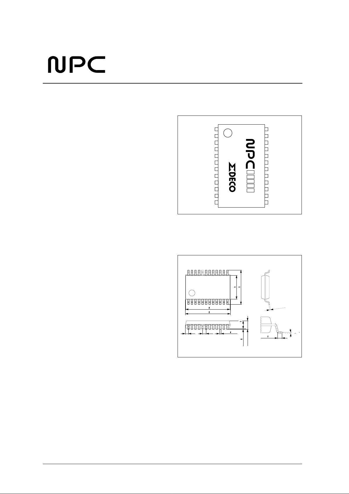
PINOUT
MLEN
DVDD
TSTN
AVDDL
1
CKSL
CKO
DVSS
BCKI
DI
LRCI XVDD
LO
12 13
LON AVSS
SM5
876
A
M
PACKAGE DIMENSIONS
Unit: mm
24-pin SSOP
7.80 0.30
5.40 0.20
10.05 0.20
10.20 0.30
0.7 0.8
0.36 0.10
1.80 0.10
2.10MAX
0.10 0.10
24
0.50 0.20
MCK
MDT
RSTN
MUTEO
XVSS
XTO
XTI
RO
AVDDR
RON
0.1
+
0.05
−
0.15
010
NIPPON PRECISION CIRCUITS—1
Page 2
BLOCK DIAGRAM
SM5876AM
LRCI DIBCKI
MLEN
MCK
MDT
RSTN
CKSL
DVSS
DVDD
TSTN
AVDDL
Microcontroller
interface
Timing
control
PWM data
generation block
Filter & attenuation
L
R
Input interface
LR
operation block
LR
Noise shaper
operation block
MUTEO
CKO
XVSS
XTO
XTI
XVDD
AVDDR
LO AVSS RON
ROLON
PIN DESCRIPTION
Number Name I/O Description
1 MLEN Ip Microcontroller control latch clock input
2 CKSL Ip 768fs/384fs clock select. 768fs when HIGH, and 384fs when LOW.
3 CKO O Oscillator clock buffer output
4 DVSS Digital ground pin
5 BCKI Ip Data bit clock input pin
6 DI Ip Serial data input pin
7 DVDD Digital supply pin
8 LRCI Ip Sample data rate (fs) clock input pin. Left channel when HIGH, and right channel when LOW.
9 TSTN Ip Test input pin
10 LO O Left-channel analog output (+)
11 AVDDL Left-channel analog supply pin
12 LON O Left-channel analog output ( − )
13 AVSS Analog ground pin
14 RON O Right-channel analog output ( − )
NIPPON PRECISION CIRCUITS—2
Page 3
−
−
+
−
+
−
°
°
−
−
−
−
−
SM5876AM
Number Name I/O Description
15 AVDDR Right-channel analog supply pin
16 RO O Right-channel analog output (+)
17 XVDD Crystal oscillator supply pin
18 XTI I Crystal oscillator or external clock input pin
19 XTO O Crystal oscillator output pin
20 XVSS Crystal oscillator ground pin
21 MUTEO O Infinity-zero detector output (analog mute control)
22 RSTN Ip Reset pin. Reset when LOW.
23 MDT Ip Microcontroller control data input pin
24 MCK Ip Microcontroller control clock input pin
I: INPUT O: OUTPUT Ip: Input with pull-up Registor
−
−
° C
SPECIFICATIONS
Absolute Maximum Ratings
DV
= AV
SS
Supply voltage range DV
Input voltage range
XTI input voltage range V
Storage temperature range T
Power dissipation P
Soldering temperature T
Soldering time t
1. Pins MLEN, CKSL, BCKI, DI, LRCI, TSTN, MCK, MDT.
Also applicable during supply switching.
Recommended Operating Conditions
5 V operation: DV
Supply voltage range DV
Supply voltage variation
Operating temperature range T
SS
= XV
= 0 V, AV
SS
DD
= AV
DDL
= AV
Parameter Symbol Rating Unit
DD
1
SS
= AV
SS
= XV
= 0 V, AV
SS
DD
= AV
Parameter Symbol Rating Unit
DD
DV
DV
XV
DV
DV
XV
DDR
, AV
, AV
DD
DD
DD
SS
SS
SS
, XV
DD
DD
V
IN1
IN
stg
D
sld
sld
= AV
opr
DDL
DD
XV
AV
AV
XV
AV
AV
, XV
DD
DD
DD
SS
SS
SS
DDR
DD
,
,
,
,
,
0.3 to 7.0 V
DV
XV
SS
SS
0.3 to DV
0.3 to XV
0.3 V
DD
0.3 V
DD
40 to 125
250 mW
255
10 s
4.5 to 5.5 V
±0.1 V
40 to 85
C
C
NIPPON PRECISION CIRCUITS—3
Page 4
SM5876AM
−
−
−
−
−
−
−
° C
3 V operation: DV
Supply voltage range DV
Supply voltage variation
Operating temperature range T
= AV
SS
Parameter Symbol Rating Unit
SS
= XV
= 0 V, AV
SS
DD
= AV
, AV
DD
DV
DD
DV
DD
XV
DD
DV
SS
DV
SS
XV
SS
DDL
DD
XV
AV
AV
XV
AV
AV
opr
DC Electrical Characteristics
5 V operation: DV
T
= − 40 to 85 ° C
a
Parameter Symbol Condition
DVDD digital supply current
XVDD system clock supply current
AVDD analog supply current
XTI HIGH-level input voltage V
XTI LOW-level input voltage V
XTI AC-coupled input voltage V
HIGH-level input voltage
LOW-level input voltage
HIGH-level output voltage
LOW-level output v oltage
CKO HIGH-level output voltage V
CKO LOW-lev el output voltage V
XTI HIGH-level input current I
XTI LOW-level input current I
LOW-level input current
Input leakage current
1. DVDD = AVDD = XVDD = 5 V, CKSL = HIGH (768fs), XTI clock input frequency f
2. Pins MLEN, CKSL, BCKI, DI, LRCI, TSTN, MCK, MDT.
3. Pins LO, LON, RO, RON,MUTEO.
= AV
SS
1
2
2
3
3
2
2
= XV
SS
1
1
= 0 V, DV
SS
I
DDD
I
DDX
I
DDA
IH1
IL1
INAC
V
IH2
V
IL2
V
OHA
V
OLA
OHC
OLC
IH1
IL1
I
IL2
I
LH
= AV
DD
Total current – 1 2 mA
Clock input 0.7XV
Clock input – – 0.3XV
IOH = −1 mA AVDD − 0.4 – – V
IOL = 1 mA – – 0.4 V
IOH = −1 mA DVDD − 0.4 – – V
IOL = 1 mA – – 0.4 V
VIN = XV
VIN = 0 V – 12 25 µA
VIN = 0 V – 12 25 µA
VIN = DV
DD
DD
DD
= AV
, XV
DD
,
DD
,
DD
,
DD
,
SS
,
SS
SS
= XV
= 33.8688 MHz, no output load, NPC-standard input data pattern.
XTI
, CKSL = LOW (384fs)
DDR
2.7 to 4.5 V
±0.1 V
20 to 70
= 4.5 to 5.5 V, AV
DD
Rating
min typ max
–1525mA
–610mA
DD
0.3XV
DD
2.4 – – V
– – 0.5 V
–1225µA
– – 1.0 µA
––V
––V
DD
= AV
DDL
DD
= AV
Unit
V
p-p
DDR
,
3 V operation: DV
T
= − 20 to 70 ° C
a
Parameter Symbol Condition
DVDD digital supply current
XVDD system clock supply current
AVDD analog supply current
XTI HIGH-level input voltage V
SS
= AV
1
1
SS
1
= XV
= 0 V, DV
SS
I
DDD
I
DDX
I
DDA
IH1
= AV
DD
Total current – 0.5 1 mA
Clock input 0.7XV
DD
= XV
= 2.7 to 4.5 V, AV
DD
Rating
min typ max
–69mA
– 1.5 3 mA
DD
––V
NIPPON PRECISION CIRCUITS—4
DD
= AV
DDL
= AV
Unit
DDR
,
Page 5

SM5876AM
Parameter Symbol Condition
Rating
min typ max
XTI LOW-level input voltage V
XTI AC-coupled input voltage V
HIGH-level input voltage
LOW-level input voltage
HIGH-level output voltage
LOW-level output v oltage
2
2
3
3
CKO HIGH-level output voltage V
CKO LOW-lev el output voltage V
XTI HIGH-level input current I
XTI LOW-level input current I
LOW-level input current
Input leakage current
2
2
V
V
INAC
V
V
OHA
OLA
OHC
OLC
IH1
I
I
IL1
IH2
IL2
IL1
IL2
LH
1. DVDD = AVDD = XVDD = 3 V, CKSL = LOW (384fs), XTI clock input frequency f
2. Pins MLEN, CKSL, BCKI, DI, LRCI, TSTN, MCK, MDT.
Clock input – – 0.3XV
0.3XV
DD
––V
2.4 – – V
– – 0.5 V
IOH = −0.5 mA AVDD − 0.4 – – V
IOL = 0.5 mA – – 0.4 V
IOH = −0.5 mA DVDD − 0.4 – – V
IOL = 0.5 mA – – 0.4 V
VIN = XV
DD
–415µA
VIN = 0 V – 4 15 µA
VIN = 0 V – 4 15 µA
VIN = DV
DD
= 16.9344 MHz, no output load, NPC-standard input data pattern.
XTI
– – 1.0 µA
3. Pins LO, LON, RO, RON,MUTEO.
AC Electrical Characteristics
5 V operation: DVSS = AVSS = XVSS = 0 V, DVDD = AVDD = XVDD = 4.5 to 5.5 V, AVDD = AV
Ta = −40 to 85 °C
DD
DDL
Unit
= AV
V
p-p
DDR
,
3 V operation: DVSS = AVSS = XVSS = 0 V, DVDD = AVDD = XVDD = 2.7 to 4.5 V, AVDD = AV
Ta = −20 to 70 °C, CKSL = LOW (384fs system clock)
System clock (XTI)
Crystal Oscillator
Parameter Symbol Condition
Oscillator frequency f
External clock input
Parameter Symbol Condition
HIGH-level clock pulsewidth t
LOW-level clock pulsewidth t
Clock pulse cycle t
OSC
CWH
CWL
XI
min typ max
768fs 8.0 33.8688 35.6 MHz
384fs 4.0 16.9344 17.8 MHz
min typ max
768fs 13.0 14.75 62.5 ns
384fs 26.0 29.5 125 ns
768fs 13.0 14.75 62.5 ns
384fs 26.0 29.5 125 ns
768fs 28.0 29.5 125 ns
384fs 56.0 59.0 250 ns
Rating
Rating
DDL
= AV
Unit
Unit
DDR
,
NIPPON PRECISION CIRCUITS—5
Page 6
XTI input clock
Serial input (BCKI, DI, LRCI)
t
CWH
SM5876AM
V
IH1
0.5V
DD
V
t
CWL
t
XI
IL1
Parameter Symbol
BCKI HIGH-level pulsewidth t
BCKI LOW-level pulse width t
BCKI pulse cycle t
DI setup time t
DI hold time t
Last BCKI rising edge to LRCI edge t
LRCI edge to first BCKI rising edge t
Serial input timing
BCKI
t
DS
BCWH
BCWL
BCY
DS
DH
t
BCWH
t
Rating
min typ max
50 – – ns
50 – – ns
1/(64fs) – – ns
50 – – ns
50 – – ns
BL
LB
t
50 – – ns
50 – – ns
BCY
t
BCWL
Unit
1.5V
DH
DI
LRCI
1.5V
t
BL
t
LB
1.5V
NIPPON PRECISION CIRCUITS—6
Page 7

Control input (MCK, MDT, MLEN)
SM5876AM
Parameter Symbol
MCK HIGH-level pulsewidth t
MCK LOW-level pulsewidth t
MCK pulse cycle t
MDT setup time t
MDT hold time t
MLEN setup time t
MLEN hold time t
MLEN level pulsewidth T
Rise time t
Fall time t
Control input timing
MCK
tMCWH
MCWH
MCWL
MCY
MDS
MDH
MLS
MLH
MLH
tMCY
Rating
min typ max
140 – – ns
140 – – ns
280 – – ns
100 – – ns
100 – – ns
1/(192fs) + 20 – – ns
1/(192fs) + 20 – – ns
1/(192fs) + 20 – – ns
r
f
––50ns
––50ns
Unit
1.5V
tMCWL
MDT
tMDH tMDS
tMLS
MLEN
tMLY
t
f
MCK
MDT
MLEN
2.4V 2.4V
0.5V 0.5V
Reset Input (RSTN)
Parameter Symbol
RSTN LOW-level pulsewidth after supply rising edge t
RSTN
tMLH
1.5V
1.5V
t
r
1.5V
Rating
min typ max
50 – – ns
Unit
NIPPON PRECISION CIRCUITS—7
Page 8

Theoretical Filter Characteristics
Deemphasis OFF overall characteristics
SM5876AM
Parameter
Frequency band Attenuation (dB)
f @ fs = 44.1 kHz min typ max
Passband ripple 0 to 0.4535fs 0 to 20.0 kHz −0.05 – +0.05
Stopband attenuation 0.5465fs to 7.4535fs 24.1 to 328.7 kHz 32 – –
Built-in analog LPF compensation 0.4535fs 20.0 kHz – −0.34 –
Overall frequency characteristic (deemphasis OFF)
0
10
20
30
Gain (dB)
40
50
60
0.0
Passband characteristic (deemphasis OFF)
0.0
0.2
0.4
Gain (dB)
0.6
0.8
Frequency (fs)
Frequency (fs)
8.07.06.05.04.03.02.01.0
0.5000.3750.2500.125 0.45350.000
NIPPON PRECISION CIRCUITS—8
Page 9

Deemphasis ON overall characteristics
SM5876AM
Parameter
Frequency band Attenuation (dB)
f @ fs = 44.1 kHz min typ max
Deviation from ideal deemphasis filter
characteristics
0 to 0.4535fs 0 to 20.0 kHz −0.09 – +0.23
Stopband attenuation 0.5465fs to 7.4535fs 24.1 to 328.7 kHz 36 – –
Built-in analog LPF compensation 0.4535fs 20.0 kHz – −0.34 –
Overall frequency characteristic (deemphasis ON)
0
10
20
30
Gain (dB)
40
50
60
0.0
Passband characteristic (deemphasis ON)
0
2
4
6
Gain (dB)
8
10
12
0.000
Frequency (fs)
Frequency (fs)
8.07.06.05.04.03.02.01.0
0.5000.3750.2500.125 0.4535
NIPPON PRECISION CIRCUITS—9
Page 10

AC Analog Characteristics
SM5876AM
5 V operation: DVSS = AVSS = XVSS = 0 V, DVDD = AVDD = XVDD = 5 V, AVDD = AV
CKSL = 0 V, deemphasis OFF, crystal oscillator frequency f
Parameter Symbol Condition
Total harmonic distortion THD + N 1 kHz, 0 dB – 0.005 0.01 %
LSI output level
Evaluation board output level V
Dynamic range D.R 1 kHz, −60 dB 88 92 – dB
Signal-to-noise ratio
Channel separation Ch. Sep 1 kHz, −∞/0 dB 84 86 – dB
1. The LSI output level = 0.3058AVDD Vrms.
2. Signal-to-noise is measured following a device reset, with DATA = 0 (DI = LOW). Under these conditions, the signal-to-noise ratio includes noise-shaper
noise.
1
2
V
out1
out2
S/N 1 kHz, 0/−∞ dB 88 92 – dB
1 kHz, 0 dB – 1.53 – V
1 kHz, 0 dB 1.8 2.0 2.2 V
= 16.9344 MHz, Ta = 25 °C
OSC
Rating
min typ max
3 V operation: DVSS = AVSS = XVSS = 0 V, DVDD = AVDD = XVDD = 3 V, AVDD = AV
CKSL = 0 V, deemphasis OFF, crystal oscillator frequency f
Parameter Symbol Condition
Total harmonic distortion THD + N 1 kHz, 0 dB – 0.007 – %
LSI output level
Evaluation board output level V
Dynamic range D.R 1 kHz, −60 dB – 90 – d B
Signal-to-noise ratio
Channel separation Ch. Sep 1 kHz, −∞/0 dB – 82 – dB
1
2
V
out1
out2
S/N 1 kHz, 0/−∞ dB –90–dB
1 kHz, 0 dB – 0.92 – V
1 kHz, 0 dB – 1.2 – V
= 16.9344 MHz, Ta = 25 °C
OSC
Rating
min typ max
DDL
DDL
= AV
= AV
DDR
DDR
,
Unit
rms
rms
,
Unit
rms
rms
1. The LSI output level = 0.3058AVDD Vrms.
2. Signal-to-noise is measured following a device reset, with DATA = 0 (DI = LOW). Under these conditions, the signal-to-noise ratio includes noise-shaper
noise.
NIPPON PRECISION CIRCUITS—10
Page 11

SM5876AM
AC Measurement Circuit and Conditions
Measurement circuit block diagram
CKO
Signal
Generator
(768fs/384fs)
BCK
LRCK(fs)
DATA
Evaluation
Board
Left Channel
Right Channel
L/R Channel
Selector
Distortion
Analyzer
fs= 44.1kHz
DATA= 16bit
10kΩ Input Impedance
NF Corporation 3346A
Measurement conditions
Parameter
Total harmonic distortion THD + N
Output level V
Dynamic range DR D-RANGE
Signal-to-noise ratio S/N THRU
Channel separation Ch. Sep THRU
1. Pins LO and RO should have an output load of 10 kΩ (min).
1
Symbol
out
3346A left/right-channel selector
switch
THRU
RMS Measurement
Shibasoku AD725C
AD725C distortion analyzer with
built-in filter
20 kHz lowpass filter ON
400 Hz highpass filter OFF
20 kHz lowpass filter ON
400 Hz highpass filter OFF
JIS A filter ON
20 kHz lowpass filter ON
400 Hz highpass filter OFF
NIPPON PRECISION CIRCUITS—11
Page 12

Measurement circuit
SM5876AM
VCC
10µ 10µ
0.01µ
+
+
0.01µ
AGND
++
0.01µ
VEE
0.01µ 10µ 10µ
AVDD
15k
AVSS
100p
100p
15k 22k
24k
100
2.2µ
−
−
R
OUTPUT
+
U3
NJM5532
+
100k
U3
NJM5532
680p
1/2
1/2
100p
15k
100p
100p
22k
15k
24k
2.2µ 100
−
−
L
OUTPUT
+
U4
+
100k
U4
1/2
NJM5532
680p
1/2
NJM5532
100p
100µ
+
0.01µ
XVDD
0.01µ
XVSS
10p
X'tal
10p
0.1µ
DVDD
DVSS
0.01µ 220µ
SW4SW3
220p
8.2k
10k
24k
+
100µ
0.1µ
+
24k
8.2k
+
100µ
0.1µ
100µ
+
8.2k
0.1µ
100µ
+
220p
10k 8.2k
10k
AVSS
RON
AVDDR
RO
XVDD
XTI
XTO
XVSS
MUTEO
RSTN
MDT
MCK
10k
LON
AVDDL
LO
TSTN
LRCI
DVDD
DI
BCKI
DVSS
SM5876
CKO
CKSL
MLEN
CKO
MUTEO
MDT
MCK
LRCI
DI
BCKI
J1
CKSL
RSTN
MLEN
NIPPON PRECISION CIRCUITS—12
Page 13

SM5876AM
FUNCTIONAL DESCRIPTION
System Clock/Speed Switching (XTI, XTO, CKO, CKSL)
The system clock on XTI can be set to run at one of
two speeds, 384fs (normal speed) or 768fs (doublespeed), where fs is the input frequency on LRCI. The
speed for CD playback is set by the input level on
CKSL, as shown in table 1.
Table 1. System clock select
Parameter Symbol
XTI input clock
frequency
CD playback XTI
frequency
CKO output clock
frequency
Internal system
clock period
f
XI
(= 1/tXI)
f
XI
f
CO
T
SYS
33.8688 MHz
at fs = 44.1
CKSL
HIGH L OW
768fs 384fs
16.9344 MHz
kHz
768fs 384fs
2t
XI
at fs = 44.1
kHz
t
XI
System Reset (RSTN)
The device should be reset in the following cases.
■ At power ON
■ When LRCI and/or the system clock XTI stop, or
other abnormalities occur.
■ When switching the XTI clock 768fs ⇔ 384fs.
Note that the input clock accuracy and signal-tonoise ratio greatly influence the AC analog characteristics. Accordingly, care should be taken to ensure
that the clock is free from jitter.
The system clock can be controlled by a crystal
oscillator comprising a crystal connected between
XTI and XTO and the built-in CMOS inverter. Alternatively, an external system clock can be input on
XTI. As the internal CMOS inverter has a feedback
resistor, the external clock can be AC coupled to
XTI. The system clock is output on CKO.
The device is reset by applying a LOW-level pulse on
RSTN. At system reset, the internal arithmetic operation and output timing counter are synchronized on
the next LRCI rising edge, as shown in figure 1.
RSTN
Low
123 910
LRCI
Internal
Reset
LO(LON)
RO(RON)
Figure 1. System reset timing
Output mute
At power-ON reset (when RSTN goes LOW), the
outputs LO (LON) and RO (RON) enter the output
mute state. Mute is released on the 9th LRCI rising
edge after RSTN goes HIGH. During this cycle, the
timing reset can cause output noise to be generated.
Output Muted
NIPPON PRECISION CIRCUITS—13
Page 14

SM5876AM
Infinity-Zero Detector (analog mute control) Output (MUTEO)
The SM5876AM outputs an infinity-zero detection
output signal under the following circumstances.
1. When an infinity-zero occurs on both the left and
right channels.
2. When an infinity-zero occurs in the input data for
the channel set by the output mode setting.
3. When the output mode setting is muting for both
the left and right channels.
4. When the attenuation counter for both the left and
right channels is 0 (−∞).
1 2 3 8 9
LRCI
DI
RSTN
MUTEO
Initialize
Figure 2. MUTEO output timing
Audio Data Input (DI, BCKI, LRCI)
Also from immediately after a reset input on RSTN
until the initialization cycle finishes and the first data
cycle occurs.
In cases 1 and 2, from when an infinity-zero is
detected a period of 214 × (1/fs) ≈ 0.37 seconds takes
place before MUTEO goes HIGH.
In cases 3 and 4, from when the attenuation counter
value is 0 a period of 214 × (1/fs) ≈ 0.37 seconds
takes place before MUTEO goes HIGH.
14
2 /fs
Signal SignalNo Signal
The digital audio data is input on DI in MSB-first,
2s-complement, 16-bit serial format.
Serial data bits are read into the SIPO register (serialto-parallel converter register) on the rising edge of
the bit clock BCKI.
The arithmetic operation and output timing are independent of the input timing. Accordingly, after a
reset, as long as the clock frequency ratio between
LRCI and the system clock XTI is maintained, phase
differences between LRCI, BCKI and the system
clock XTI do not affect the functional operation.
Also, any jitter present on the data input clock does
not appear as output pulse jitter.
The bit clock frequency on BCKI should be between
32fs and 64fs.
Operating Modes (MLEN, MDT, MCK)
The microcontroller data is used to control the following parameters.
Digital attenuator
Digital attenuation is controlled by attenuation data
input on MDT.
The attenuation operation is determined by a mathematical operation of the internal 8-bit up/down
counter’s output data on the signal data. The 8-bit
up/down counter, when attenuation data is input on
MDT, can control the left and right channels either
independently or together (independent when the
MDT attenuation control flag is LOW, and together
when HIGH).
The left-channel counter contents DATTL and the
right-channel counter contents DATTR control the
left-channel gain and right-channel gain, respectively, using the following equations.
DATTL
Left-channel
Right-channel
gain 20
×
×
gain 20
-------------------
log
255
DATTR
------------------- -
log
255
[dB]=
[dB]=
After system reset initialization, independent
left/right-channel attenuation mode with the maximum gain of 0 dB is the default.
Deemphasis filter (MDT DEM flag)
The built-in digital deemphasis filter is designed to
operate at 44.1 kHz. Deemphasis is ON when the
DEM flag is HIGH, and OFF when the DEM flag is
LOW. After reset, deemphasis OFF is the default.
NIPPON PRECISION CIRCUITS—14
Page 15

SM5876AM
Output mode setting (MDT 4-bit data)
The left-channel and right-channel outputs can be set
to any one of 16 different modes, as shown in table 2.
Table 2. Output mode control
PL0 PL1 PL2 PL3 Left-channel output Right-channel output Notes
0000 Mute Mute Mute
0001 Mute R
0010 Mute L
0011 Mute (L + R)/2
0100 R Mute
0101 R R
0110 R L Reverse
0111 R (L + R)/2
1000 L Mute
1001 L R Stereo
1010 L L
1011 L (L + R)/2
1100 (L + R)/2 Mute
1101 (L + R)/2 R
1110 (L + R)/2 L
1111 (L + R)/2 (L + R)/2
“Stereo” is the default after system reset.
“Mute” refers to soft muting.
Soft mute (output mode setting)
The channel output muting set by the output mode
control 4-bit data is soft mute mode.
The attenuation counter output decrements by 1 step
at a time, reducing the gain. The signal is completely
muted after a time of (1024/fs), which corresponds to
approximately 23.2 ms when fs = 44.1 kHz.
Conversely, when soft mute is released using the output mode control, the attenuation counter output
increments by 1 step at a time, increasing the gain.
The time taken to return to 0 dB from full muting is
Upon system reset initialization, mute is released,
which corresponds to the maximum gain of 0 dB.
MUTE
0 dB
Gain
– ∞
1024/fs 1024/fs
Figure 3. Soft mute operation example
also (1024/fs).
When an attenuation value is set, the output gain
decreases from the value set by the attenuation data
until the gain is − ∞ . Similarly for mute release, the
output gain increases from the current value until the
gain is 0 dB.
Attenuator control (ATC flag)
The attenuator control (ATC) flag is input on MDT.
When the ATC flag is HIGH, the left-channel and
right-channel attenuator data is common. In this
mode, the left-channel data is used for both channels.
Soft mute operation is shown in figure 3.
NIPPON PRECISION CIRCUITS—15
Page 16

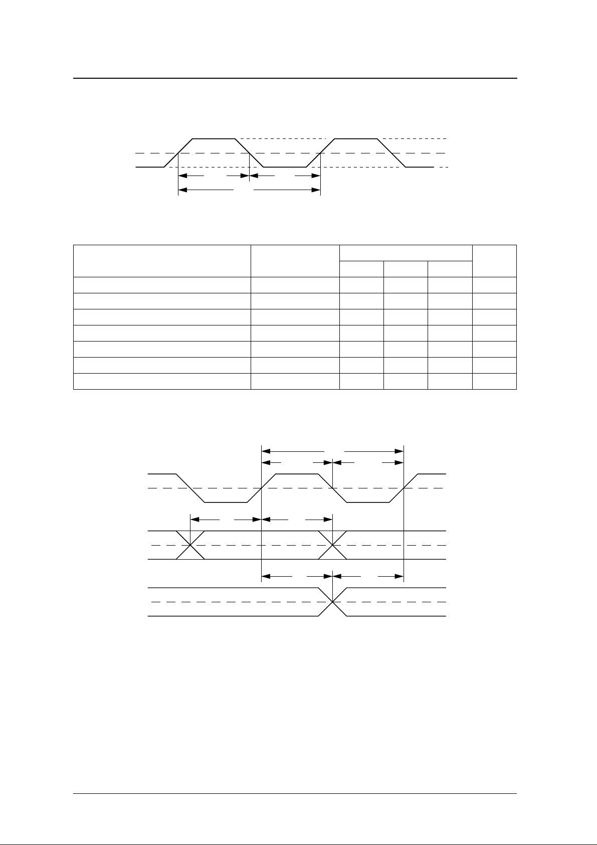
TIMING DIAGRAMS
Input Timing
(DI, BCKI, LRCI)
Left
Channel
DI
BCKI
(64fs MAX)
LRCI
(MDT, MCK, MLEN)
SM5876AM
1/fs
LSB
Right
Channel
16 bit
MSB
16 bit
MSB LSB
MCK
MDATA
MLEN
L channel
Attenuation Data
LSB MSB LSB MSB
Data is recognized on the rising edge of MLEN.
R channel
Attenuation Data
13 12 11 10 9 8 7 6 5 4 3 2 1 018 17 16 15 1423 22 21 20 19
Output
Mode Control
PL0 PL1 PL2 PL3 DEM ATC
NIPPON PRECISION CIRCUITS—16
Page 17

SM5876AM
TYPICAL APPLICATIONS
Input Interface Circuit
X'tal
XTI XTO
CKO
44.1kHz
2.1168MHz
Note that the output analog characteristics and other specifications are not guaranteed for a particular format or
application circuit.
Output Analog Processing Circuit
LRCI
DI
BCKI
SM5876
(Left channel only is shown.)
LON
SM5876
LO
NIPPON PRECISION CIRCUITS INC. reserves the right to make changes to the products described in this data sheet in order to
improve the design or performance and to supply the best possible products. Nippon Precision Circuits Inc. assumes no responsibility for
the use of any circuits shown in this data sheet, conveys no license under any patent or other rights, and makes no claim that the circuits
are free from patent infringement. Applications for any devices shown in this data sheet are for illustration only and Nippon Precision
Circuits Inc. makes no claim or warr anty that such applications will be suitab le for the use specified without further testing or modification.
The products described in this data sheet are not intended to use for the apparatus which influence human lives due to the failure or
malfunction of the products. Customers are requested to comply with applicable laws and regulations in effect now and hereinafter,
including compliance with export controls on the distribution or dissemination of the products. Customers shall not expor t, directly or
indirectly, any products without first obtaining required licenses and approvals from appropriate government agencies.
−
+
LOUT
NIPPON PRECISION CIRCUITS INC.
NIPPON PRECISION CIRCUITS INC.
4-3, 2-chome Fukuzumi
Koutou-ku, Tokyo 135-8430, Japan
Telephone: 03-3642-6661
Facsimile: 03-3642-6698
NC9504BE 1996.06
NIPPON PRECISION CIRCUITS—17
 Loading...