

Page 1
SM5852CS
NIPPON PRECISION CIRCUITS—1
NIPPON PRECISION CIRCUITS INC.
Dynamic Range Compression LSI
OVERVIEW
The SM5852CS is a digital signal processor IC that
performs dynamic range compression for use in
digital audio reproduction equipment. It is designed
for use with a 44.1 kHz sampling frequency.
FEATURES
■
2-channel processing
■
6 input-level dependent dynamic gain
characteristics
■
Dynamic range compression bypass mode
■
2 attack time settings
■
Soft muting function
■
Serial input/output interface
2s complement, MSB first, 16-bit
■
384fs system clock
■
23 × 23-bit multiplier/30-bit high-precision
accumulator
■
TTL-compatible input/output
■
3.2 to 5.5 V operating voltage range
■
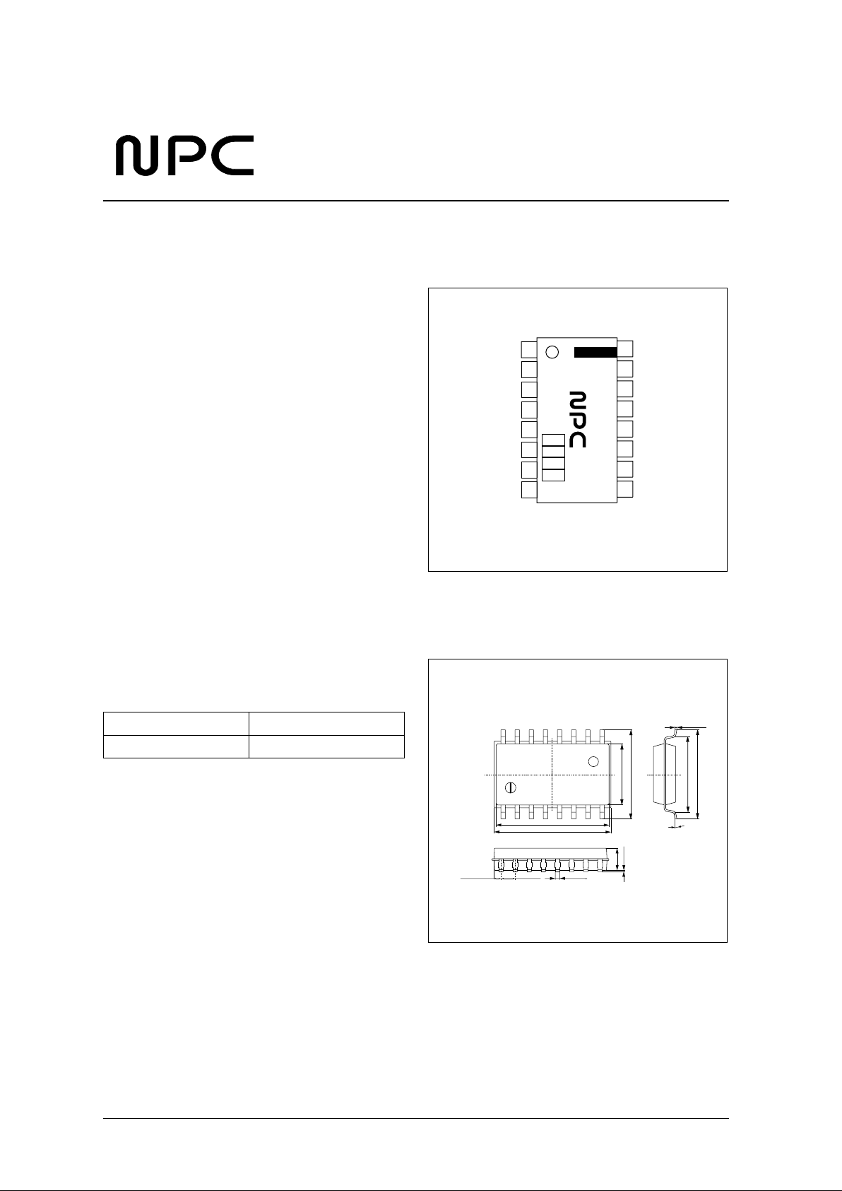
16-pin SOP
■
Molybdenum-gate CMOS
ORDERING INFOMATION
PINOUT
PACKAGE DIMENSIONS
16-pin SOP (Unit: mm)
Device Package
SM5852CS 16pin SOP
MUTEN
CLK
VSS
BCKI
DI
LRCI
RSTN
LRCO
VDD
DB/DS
TESTN
MOD2
MOD1
OPT
BCKO
DOUT
1
2
3
4
5
6
7
8
16
15
14
13
12
11
10
9
SM5852CS
10.16±0.3
10.5 MAX
8.0±0.3
5.5±0.3
0.4±0.15
1.27±0.15
0.635±0.15
2.0±0.2
0.1±0.1
0.17±0.05
8.0±0.3
6.8±0.3
0˚ to 15˚
Page 2
SM5852CS
NIPPON PRECISION CIRCUITS—2
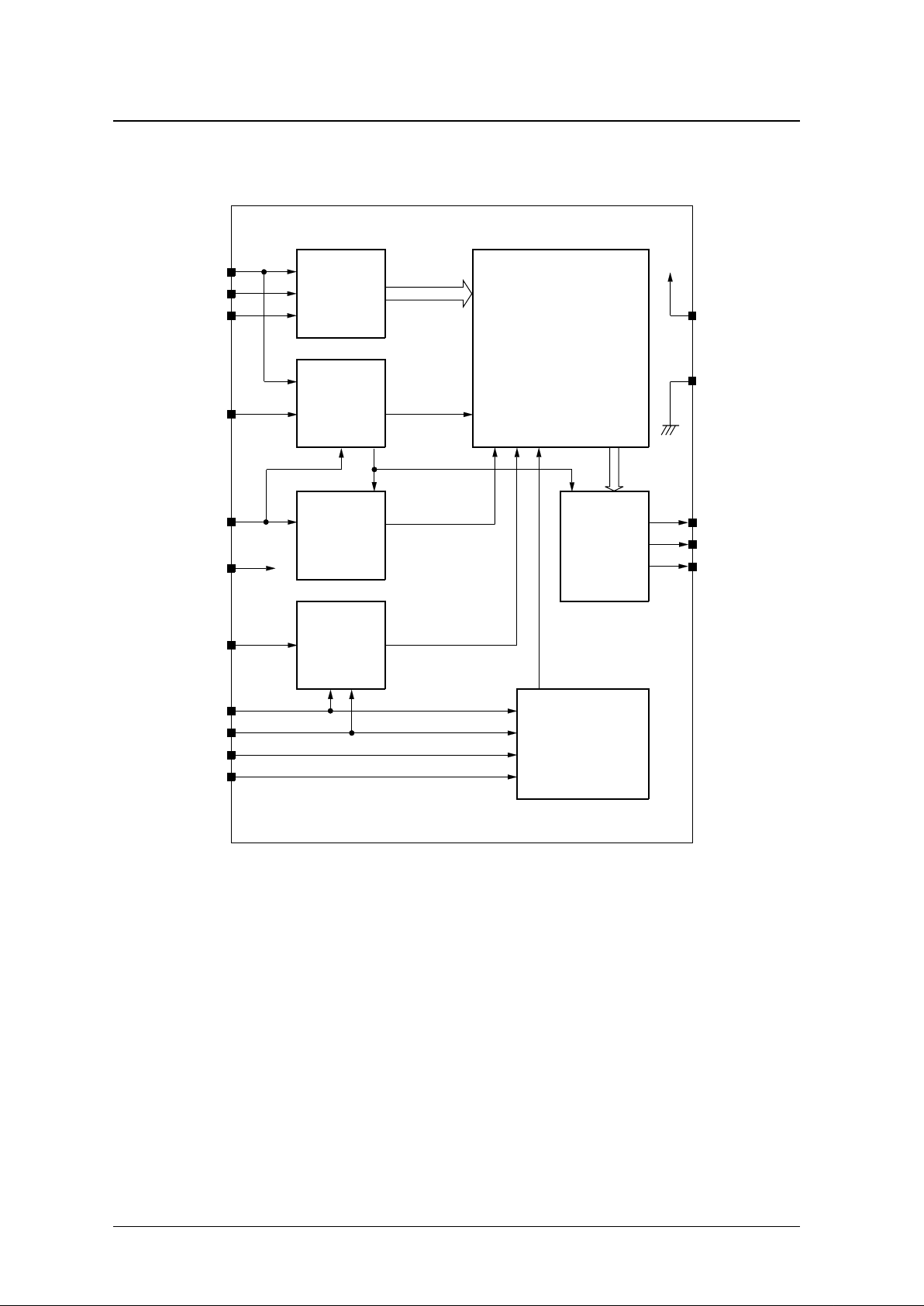
BLOCK DIAGRAM
Input data
Interface
System
Clock
Output data
Interface
Mode Control
Mute
Control
VDD
VSS
LRCO
BCKO
DOUT
Sequence
Control
DSP Block
LRCI
BCKI
DI
CLK
TESTN
MUTEN
DB/DS
OPT
MOD1
MOD2
RSTN
Page 3
SM5852CS
NIPPON PRECISION CIRCUITS—3
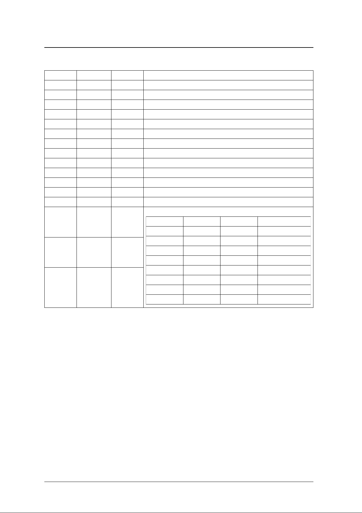
PIN DESCRIPTION
Number Name I/O
1
1. Ip = Input pin with pull-up resistor. Accordingly, they can be left open f or HIGH-level input.
Description
1 LRCI Ip Input data sample rate (fs) clock input
2 BCKI Ip Bit clock input
3 DI Ip Serial data input
4 CLK I Clock inpu t
5 VSS – Ground
6 RSTN Ip System reset initialization. Reset when LOW.
7 TESTN Ip Test mode input. Testing when LOW.
8 MUTEN Ip Mute input. Muting when LOW.
9 DOUT O Serial data output
10 BCKO O Bit clock output
11 LRCO O Output data sample rate (fs) clock output
12 VDD – 3.2 to 5.5 V supply
13 OPT Ip Attack time switch input. Attack-1 when HIGH, and attack-2 when LOW.
14 MOD1 Ip
Gain characteristics switch inputs.
15 MOD2 Ip
16 DB/DS Ip
DB/DS MOD2 MOD1 Compression mode
LOW LOW LOW 6
LOW LOW HIGH 5
LOW HIGH L OW 4
LOW HIGH HIGH Off
HIGH LOW LOW 3
HIGH LOW HIGH 2
HIGH HIGH LOW 1
HIGH HIGH HIGH Off
Page 4
SM5852CS
NIPPON PRECISION CIRCUITS—4
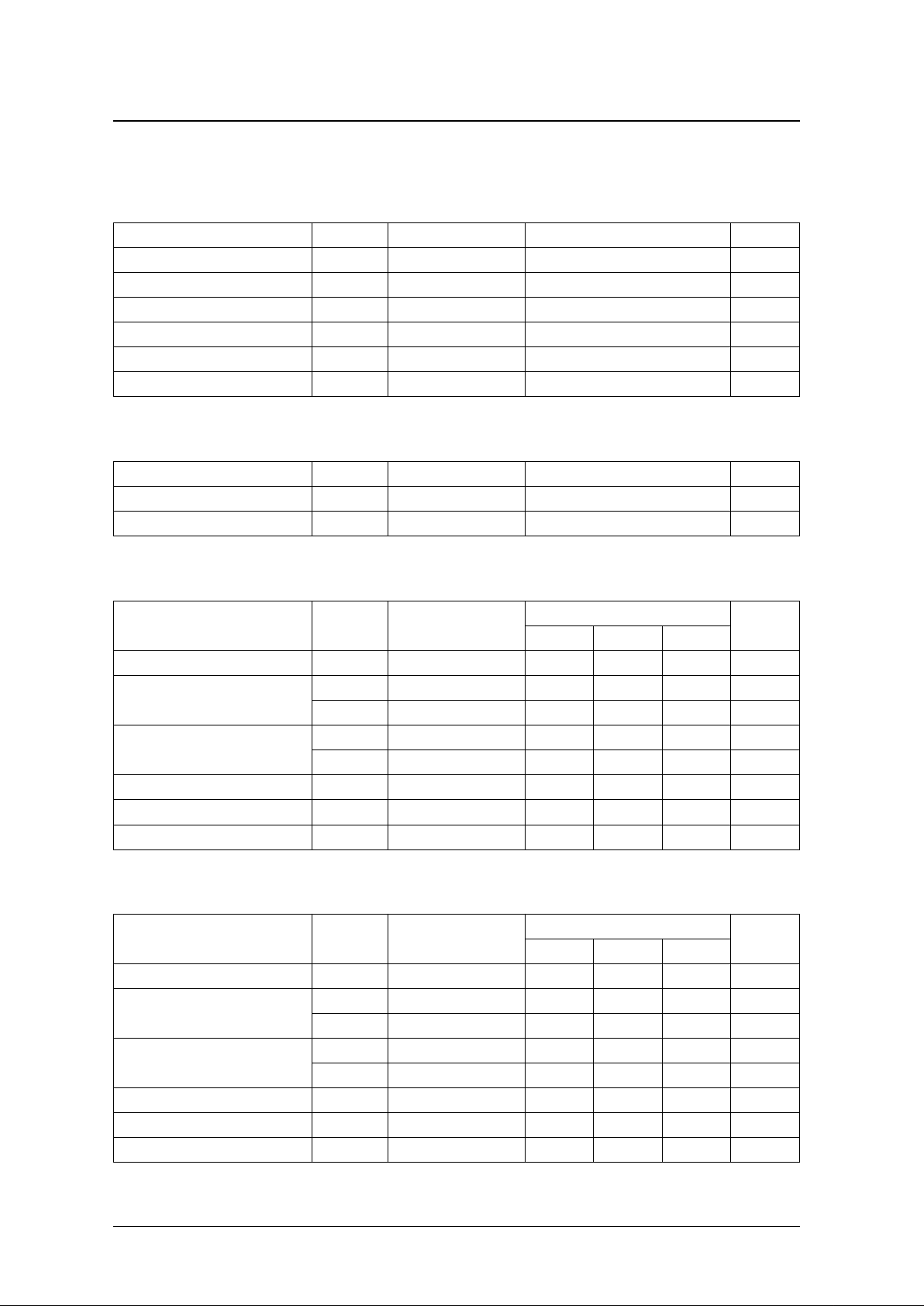
SPECIFICATIONS
Absolute Maximum Ratings
VSS = 0 V
Recommended Operating Conditions
VSS = 0 V
DC Characteristics
Standard voltage: VDD = 4.5 to 5.5 V, VSS = 0 V, Ta = −35 to 85 °C
Low voltage: VDD = 3.2 to 4.5 V, VSS = 0 V, Ta = −20 to 70 °C
Parameter Symbol Condition Rating Unit
Supply voltage V
DD
−
0.3 to 7.0 V
Input voltage V
IN
VSS − 0.3 to VDD + 0.3 V
Storage temperature T
stg
−
40 to 125
°
C
Power dissipation P
D
250 mW
Soldering temperature T
sld
255
°
C
Soldering time t
sld
10 s
Parameter Symbol Condition Rating Unit
Supply voltage V
DD
3.2 to 5.5 V
Operating temperature T
opr
−
35 to 85
°
C
Parameter Symbol Condition
Rating
Unit
min typ max
Current consumption
1
1. f
CLK
= 384fs = 16.9344 MHz, no output load, input data conformance with NPC test pattern
I
DD
VDD = 5.0 V – 16 23 mA
Input voltage for all inputs
V
IH
2.4 – – V
V
IL
– – 0.5 V
Output voltage for all outputs
V
OH
IOH = −0.4 mA 2.5 – – V
V
OL
IOL = 1.6 mA – – 0.4 V
Input leakage current for all inputs I
LH
VIN = V
DD
– – 1.0 µA
CLK input leakage current I
LL
VIN = 0 V – – 1.0 µA
Input current for all inputs except CLK I
IL
VIN = 0 V – – 20 µA
Parameter Symbol Condition
Rating
Unit
min typ max
Current consumption
1
1. f
CLK
= 384fs = 16.9344 MHz, no output load, input data conformance with NPC test pattern
I
DD
VDD = 3.4 V – 7 10 mA
Input voltage for all inputs
V
IH
2.4 – – V
V
IL
– – 0.5 V
Output voltage for all outputs
V
OH
IOH = −0.2 mA 2.5 – – V
V
OL
IOL = 0.8 mA – – 0.4 V
Input leakage current for all inputs I
LH
VIN = V
DD
– – 1.0 µA
CLK input leakage current I
LL
VIN = 0 V – – 1.0 µA
Input current for all inputs except CLK I
IL
VIN = 0 V – – 12 µA
Page 5
SM5852CS
NIPPON PRECISION CIRCUITS—5
AC Characteristics
Standard voltage: VDD = 4.5 to 5.5 V, VSS = 0 V, Ta = −35 to 85 °C
Low voltage: VDD = 3.2 to 4.5 V, VSS = 0 V, Ta = −20 to 70 °C
CLK (384fs)
RSTN
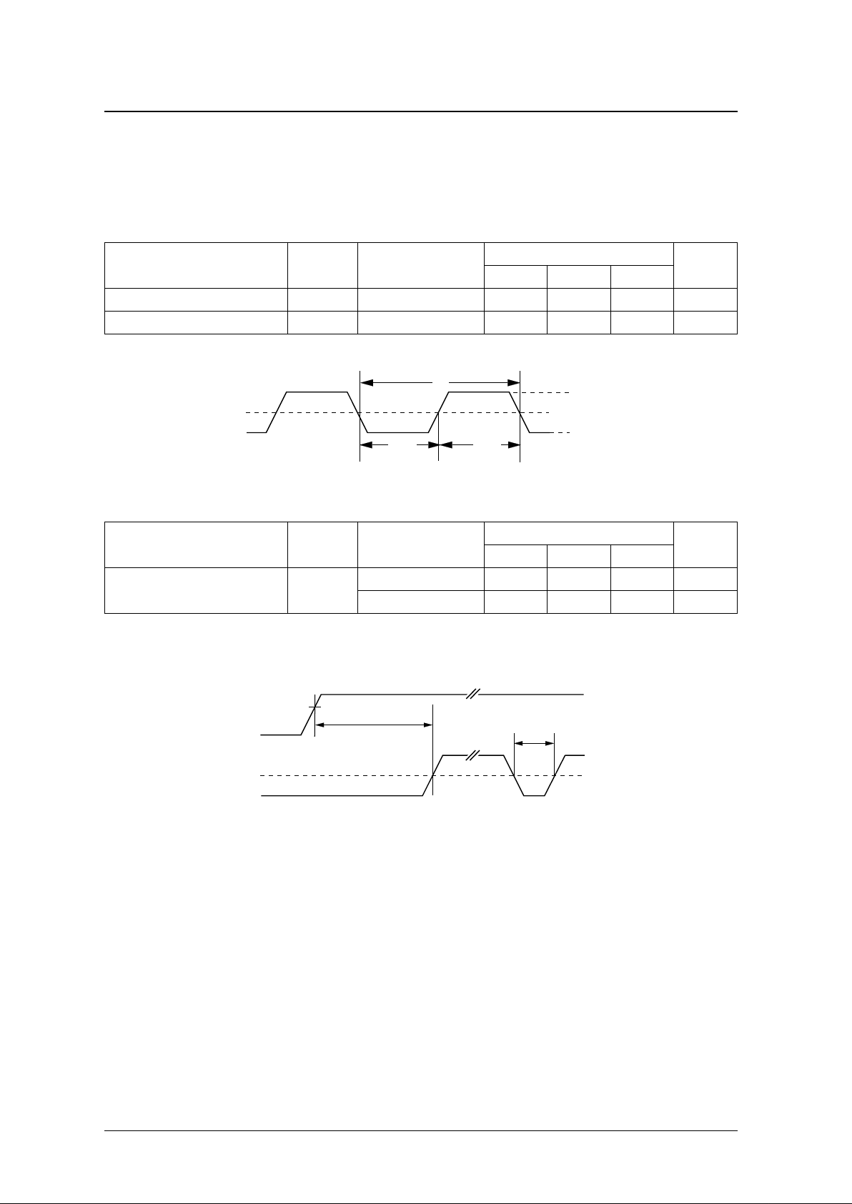
RSTN should be set LOW at power-ON and after
reacquiring synchronization. Note that if RSTN is
LOW for longer than 1 µs, a through-current flows in
the internal dynamic circuits because the internal
clock is stopped. The through-current has no rated
value, so the reset pulse should be kept as short as
possible at all times other than at power-ON.
Parameter Symbol Condition
Rating
Unit
min typ max
Clock pulsewidth t
CW
24 – 500 ns
Clock cycle time t
CY
55 59 1000 ns
tcy
tCW
CLK
1.5V
VIH
VIL
tCW
Parameter Symbol Condition
Rating
Unit
min typ max
Reset LOW-level pulsewidth t
RST
At power-ON 1 – – µs
At all other times 50 – 1000 ns
RSTN
1.5V
VDD
tRST
tRST ≥ 1µsec
3.2V
Page 6
SM5852CS
NIPPON PRECISION CIRCUITS—6
Serial input timing
DB/DS, OPT
When DB/DS or OPT change state, the input level
must be constant for a minimum of 2/fs (2 × LRCI
cycle time). Input levels of duration less than 2/fs
may be ignored.
Parameter Symbol Condition
Rating
Unit
min typ max
BCKI pulsewidth t
BCIW
100 – – ns
BCKI cycle time t
BCIY
200 – – ns
DI setup time t
DIS
75 – – ns
DI hold time t
DIH
75 – – ns
LRCI setup time t
LIS
75 – – ns
LRCI hold time t
LIH
75 – – ns
DI
1.5V
BCKI
LRCI
tBCIW tBCIW
tBCIY
tDIS
tLIS
tLIH
1.5V
1.5V
tDIH
Parameter Symbol Condition
Rating
Unit
min typ max
Minimum pulsewidth t
W
2/fs – – ns
Page 7

SM5852CS
NIPPON PRECISION CIRCUITS—7
Serial output timing
Parameter Symbol Condition
Rating
Unit
min typ max
BCKO pulsewidth t
BCOW
15 pF load 180 1/96fs – ns
BCKO cycle time t
BCOY
15 pF load 400 1/48fs – ns
DOUT, LRCO output delay time
t
DHL
15 pF load
−
20 – 60 ns
t
DLH
15 pF load
−
20 – 60 ns
DOUT
1.5V
BCKO
LRCO
tBCOW
tBCOY
1.5V
tDHL tDLH
tBCOW
Page 8

SM5852CS
NIPPON PRECISION CIRCUITS—8
Dynamic Compression Characteristics
Compression mode 1 (DB/DS = HIGH, MOD2 = HIGH, MOD1 = LOW)
Compression Compression ratio Input level Output level
Mode 1 30 dB
≤ −
60 dB +20 dB linear relative to input
−
60 to 0 dB
−
40 to −10 dB
-90
-80
-70
-60
-50
-40
-30
-20
-10
0
-90 -80 -70 -60 -50 -40 -30 -20 -10 0
Input (dB)
Output(dB)
COMP1
OFF
Page 9

SM5852CS
NIPPON PRECISION CIRCUITS—9
Compression mode 2 (DB/DS = HIGH, MOD2 = LOW, MOD1 = HIGH)
Compression Compression ratio Input level Output level
Mode 2 19 dB
≤ −
38 dB +15 dB linear relative to input
−
38 to 0 dB
−
23 to −4 dB
-90
-80
-70
-60
-50
-40
-30
-20
-10
0
-90 -80 -70 -60 -50 -40 -30 -20 -10 0
Input (dB)
Output(dB)
COMP2
OFF
Page 10

SM5852CS
NIPPON PRECISION CIRCUITS—10
Compression mode 3 (DB/DS = HIGH, MOD2 = LOW, MOD1 = LOW)
Compression Compression ratio Input level Output level
Mode 3 18 dB
≤
−54 dB +0 dB linear relative to input
−54 to −18 dB −54 to −36 dB
−18 to 0 dB −36 to −18 dB
-90
-80
-70
-60
-50
-40
-30
-20
-10
0
-90 -80 -70 -60 -50 -40 -30 -20 -10 0
Input (dB)
Output (dB)
COMP3
OFF
Page 11

SM5852CS
NIPPON PRECISION CIRCUITS—11
Compression mode 4 (DB/DS = LOW, MOD2 = HIGH, MOD1 = LOW)
Compression Compression ratio Input level Output level
Mode 4 20 dB
≤
−40 dB +15 dB linear relative to input
−40 to 0 dB −25 to −5 dB
-90
-80
-70
-60
-50
-40
-30
-20
-10
0
-90 -80 -70 -60 -50 -40 -30 -20 -10 0
Input (dB)
Output(dB)
COMP4
OFF
Page 12

SM5852CS
NIPPON PRECISION CIRCUITS—12
Compression mode 5 (DB/DS = LOW, MOD2 = LOW, MOD1 = HIGH)
Compression Compression ratio Input level Output level
Mode 5 15 dB
≤
−40 dB +15 dB linear relative to input
−40 to −10 dB −25 to −10 dB
−10 to 0 dB +0 dB linear relative to input
-90
-80
-70
-60
-50
-40
-30
-20
-10
0
-90 -80 -70 -60 -50 -40 -30 -20 -10 0
Input (dB)
Output(dB)
COMP5
OFF
Page 13

SM5852CS
NIPPON PRECISION CIRCUITS—13
Compression mode 6 (DB/DS = LOW, MOD2 = LOW, MOD1 = LOW)
Compression Compression ratio Input level Output level
Mode 6 18 dB
≤
−54 dB +18 dB linear relative to input
−54 to −18 dB −36 to −18 dB
−18 to 0 dB +0 dB linear relative to input
-90
-80
-70
-60
-50
-40
-30
-20
-10
0
-90 -80 -70 -60 -50 -40 -30 -20 -10 0
Input (dB)
Output(dB)
COMP6
OFF
Page 14

SM5852CS
NIPPON PRECISION CIRCUITS—14
Filter Characteristics
Attack-1 filter
Attack-2 filter
Frequency
(Hz)
-100
-90
-80
-70
-60
-50
-40
-30
-20
-10
0
+10
Attenuation (dB)
1.0 10 100 1K 10K 100K2.0 5.0 20 50 200 500 2k 5k
20k
50k
1.0 10 100 1K 10K 100K
Frequency
(Hz)
-100
-90
-80
-70
-60
-50
-40
-30
-20
-10
0
+10
Attenuation (dB)
2.0 5.0 20 50 200 500 2k 5k
20k
50k
Page 15

SM5852CS
NIPPON PRECISION CIRCUITS—15
FUNCTIONAL DESCRIPTION
Dynamic Range Compression
Dynamic range compression varies the effective
amplification of the input as a function of the input
signal level. The mode control block selects one of 6
dynamic range compression characteristics
according the states of DB/DS, MOD1 and MOD2.
Also, dynamic range compression can be turned
OFF, bypassing all processing.
Attack Time Selection
The input interface block incorporates a peak hold
circuit to determine the input level. The peak hold
circuit has a time constant of τ = 250 ms, and the
peak hold output is attenuated and then compared
with the next input level. Therefore, the dynamic
range compression recovery time constant is
effectively τ = 250 ms.
The attack time coefficient of the input signal, to
pass through the selected attack time LPF, is
determined by the input level.
Two attack time low-pass filter characteristics are
available, selected by the state of OPT.
■ OPT = HIGH, Attack-1 characteristics, f
C
= 350
Hz, 2nd-order LPF (Q = 0.5)
■ OPT = LOW, Attack-2 characteristics, f
C
= 150
Hz, 2nd-order LPF (Q = 0.5)
The attack time is the time required by the circuit to
return to the set value after a sudden increase in the
input. The recovery time is the time required by the
circuit to return to the set value after a sudden
decrease in the input.
Soft Muting
Soft muting is active when MUTEN is LOW. When
MUTEN is LOW, the attenuation changes smoothly
from 0 to −∞ dB in 1024/fs, or approximately 23.2
ms.
When MUTEN goes HIGH, soft muting is released
and the attenuation changes smoothly from −∞ to 0
dB, again taking approximately 23.2 ms.
Also, if a MUTEN transition occurs while the
attenuation is changing, the attenuation then changes
smoothly in the direction specified by the new level
of MUTEN.
DB/DS, OPT Switching Shock Noise
The soft muting function is also activated to
eliminate switching shock noise when DB/DS or
OPT change state. When DB/DS or OPT change
state, the attenuation changes to −∞ dB, the internal
circuit settings are activated and then soft muting is
released. Therefore, a maximum time of
approximately 46.4 ms is required to change the
compression mode. Of course, if the attenuation is
already −∞ dB after soft muting using MUTEN, then
no time is required to change compression mode.
Reset Initialization
RSTN should be set LOW at power-ON and after
reacquiring synchronization. Note that if RSTN is
LOW for longer than 1 µs, a through-current flows in
the LSI’s internal dynamic circuits because the
internal clock is stopped. The through-current has no
rated value, so the reset pulse should be kept as short
as possible at all times other than at power-ON.
When RSTN goes from LOW to HIGH, initialization
hold is released and the initialization routine first
resets the internal data over an interval of 4fs. During
the initialization routine, the output data is forcibly
muted so that there is no output signal.
DB/DS MOD2 MOD1 Compression mode
LOW LOW LOW 6
LOW LOW HIGH 5
LOW HIGH LOW 4
LOW HIGH HIGH Off
HIGH L OW LOW 3
HIGH L OW HIGH 2
HIGH HIGH LOW 1
HIGH HIGH HIGH Off
Page 16

SM5852CS
NIPPON PRECISION CIRCUITS—16
INPUT/OUTPUT TIMING
Input Timing
There must be a minimum of 16 BCKI clock cycles to read in a single word of data.
Data on DI is input in sync with the falling edge of BCKI in 16-bit serial, MSB first, 2s complement
format.
Output Timing
Shaded areas represent intervals of invalid data.
BCKO
LRCO
DOUT
MSB MSB
Lch
LSB
Rch
LSB
,
,
BCKI
LRCI
DI
MSB MSB
Lch
LSB
Rch
LSB
Page 17

SM5852CS
NIPPON PRECISION CIRCUITS—17
NIPPON PRECISION CIRCUITS INC. reserves the right to make changes to the products described in this data sheet in order to
improve the design or performance and to supply the best possible products. Nippon Precision Circuits Inc. assumes no responsibility for
the use of any circuits shown in this data sheet, conveys no license under any patent or other rights, and makes no claim that the circuits
are free from patent infringement. Applications for any devices shown in this data sheet are for illustration only and Nippon Precision
Circuits Inc. makes no claim or warr anty that such applications will be suitab le for the use specified without further testing or modification.
The products described in this data sheet are not intended to use for the apparatus which influence human lives due to the failure or
malfunction of the products. Customers are requested to comply with applicable laws and regulations in effect now and hereinafter,
including compliance with export controls on the distribution or dissemination of the products. Customers shall not expor t, directly or
indirectly, any products without first obtaining required licenses and approvals from appropriate government agencies.
NIPPON PRECISION CIRCUITS INC.
4-3, 2-chome Fukuzumi
Koto-ku, Tokyo 135-8430, Japan
Telephone: 03-3642-6661
Facsimile: 03-3642-6698
NC9622AE 1997.03
NIPPON PRECISION CIRCUITS INC.
APPLICATON CIRCUIT
SM5852CS
CKO
XTI XTO
LRCI
BCKI
DIN
DB/DS
MOD2
MOD1
OPT
LRCI
BCKI
DI
CLK
SM5871
RSTN
TESTN
MUTEN
XTAI
LRCK
C210
DATA
SONY
CXD1125
PSSL SLOB
X ' lal(16.9344 MHz)
Microcontroler
LRCO
BCKO
DOUT
1130
1135
 Loading...