

Page 1

SM5849AF
NIPPON PRECISION CIRCUITS INC.
Asynchronous Sample Rate Converter
OVERVIEW
The SM5849AF is a digital audio signal, asynchronous sample rate converter LSI. It supports 16/20/24-bit
word length input data, 16/20/24-bit word length output data, 2kHz to 100kHz input sample rate range, and
4kHz to 200kHz output sample rate range. It also features a built-in digital deemphasis filter and digital attenuator.
FEATURES
Functions
■
Left/right-channel processing (stereo)
■
2 to 100kHz input sample rate range (fsi)
■
4 to 200kHz output sample rate range (fso)
■
0.45 to 2.2-times variable sample rate conversion
ratio (fso/fsi)
■
Asynchronous input and output timing (clock
inputs)
System clock inputs (input and output clocks inde-
■
pendent)
• 256fsi or 384fsi input system clock select
• 256fso or 384fso output system clock select
Deemphasis filter
■
• IIR-type filter
• 44.1, 48 or 32kHz
Digital attenuator
■
• 11-bit data, 1025 levels
• Smooth attenuation change
• +12dB gain shift function
Direct mute function
■
Through mode operation
■
• Direct connection from input to output
Output data clocks (LRCO, BCKO)
■
• Slave mode: external input
• Master mode: output system clock generated
internally
Dither round-off processing
■
• Dither round-off ON/OFF selectable
3.3V single supply
■
80-pin QFP
■
Silicon-gate CMOS process
■
Filter Characteristics and Converter Efficiency
■
24-bit internal data word length
■
Deemphasis filter characteristics (IIR filter)
• ±0.03dB gain deviation from ideal filter characteristics
■
Anti-aliasing LPF characteristics
• Output/input sample rate conversion ratio automatic filter select (6 FIR filters)
- Up converter LPF
1.0 to 2.2 times
- Down converter LPF I
0.92 times: 48.0 to 44.1kHz
- Down converter LPF II
0.73 times: 44.1 to 32.0kHz
- Down converter LPF III
0.67 times: 48.0 to 32.0kHz
- Down converter LPF IV
0.5 times: 48.0 to 24.0kHz
- Down converter LPF V
0.45 times: 48.0 to 22.1kHz
• ±0.00005dB passband ripple
• > 110dB stopband attenuation
Converter noise levels
■
• ≤ − 110dB internal calculation (quantization)
noise
• − 98dB (16-bit output), − 122dB (20-bit output),
and − 146dB (24-bit output) word rounding
noise
Output S/N ratio (theoretical values)
■
Output signal
w ord length
16 bits 94.8dB 97.7dB 97.7dB
20 bits 97.7dB 109.5dB 109.7dB
24 bits 97.7dB 109.7dB 110dB
16-bit input
w ord length
S/N ratio
20-bit input
w ord length
24-bit input
w ord length
NIPPON PRECISION CIRCUITS—1
Page 2
Interfaces
SM5849AF
Input data format
■
• 2s-complement, L/R alternating, serial
• IIS/non-IIS format
Mode Word length Data position
1
2 Right justified LSB first
16 bits
3 Left justified MSB first
4 IIS MSB first
5
6 Right justified LSB first
20 bits
7 Left justified MSB first
8 IIS MSB first
9
10 Right justified LSB first
24 bits
11 Left justified MSB first
12 IIS MSB first
Right justified MSB first
Right justified MSB first
Right justified MSB first
APPLICATIONS
Data
sequence
Output data format
■
• 2s-complement, MSB first, L/R alternating,
serial
• Continuous bit clock
Mode Word length IIS selection Data position
1 16 bits
Right justified2 20 bits
Left justified
3 24 bits
4 24 bits
5 16 bits
7 24 bits
Normal
(non IIS)
IIS6 20 bits
Digital audio equipment-interface sample rate
■
conversion (AV amplifiers, CD-R, DAT, MD and
8mm VTRs)
ORDERING INFORMATION
De vice Pack ag e
SM5849AF 80-pin QFP
Commercial recording/editing equipment sample
■
rate conversion
NIPPON PRECISION CIRCUITS—2
Page 3
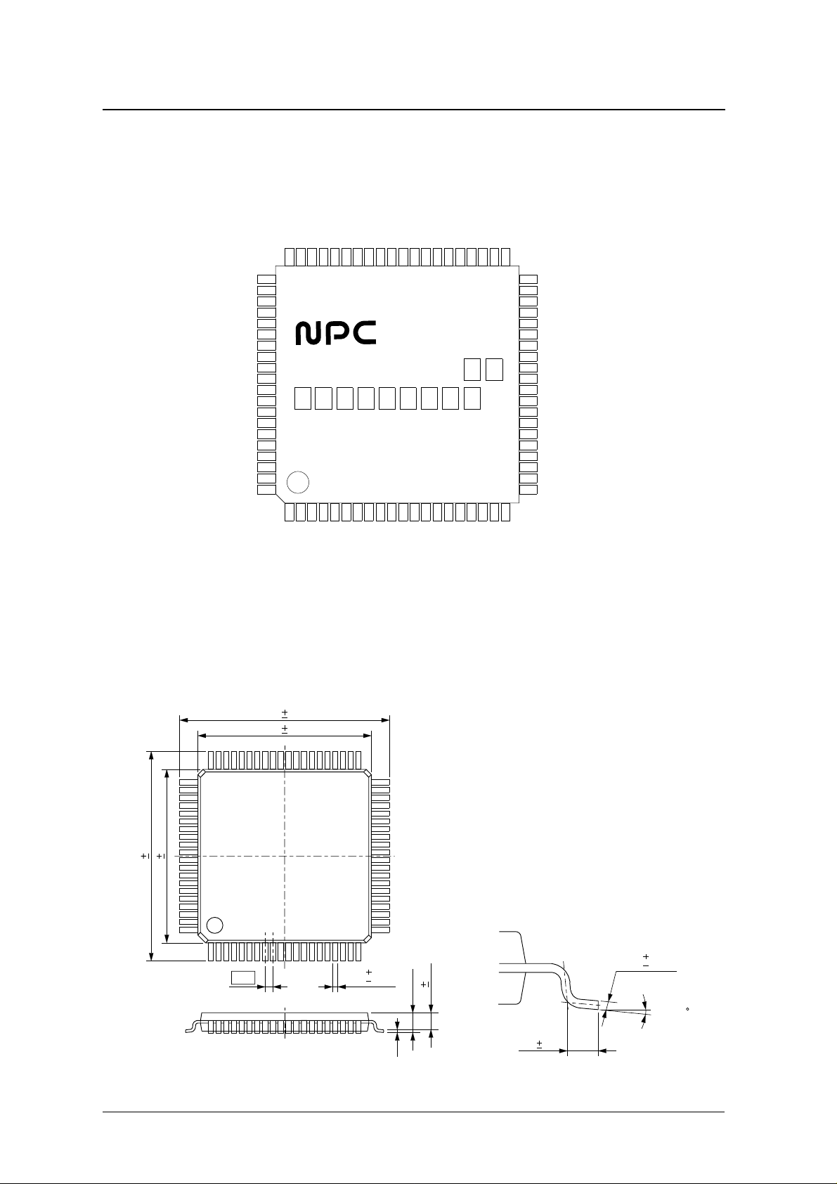
PINOUT
VDD
OCKSL
OCLK
VSS
LRCO
BCKO
DOUT
N.C.
N.C.
N.C.
N.C.
N.C.
N.C.
N.C.
N.C.
N.C.
N.C.
N.C.
N.C.
VSS
605958575655545352
61
62
63
64
65
66
67
68
69
SM5849AF
70
71
72
73
74
75
76
77
78
79
80
1
N.C.
2DI3
N.C.
4
N.C.
5
N.C.
6
SM5849AF
Top view
N.C.
N.C.
N.C.
N.C.
N.C.
SLAVE
5150494847464544434241
JAPAN
7
8
10
THRUN
RSTN
DITHN
12
TST2N
STATE
IISN
OWL1
OWL2
VDD
20
40
39
38
37
36
35
34
33
32
31
30
29
28
27
26
25
24
23
22
21
VSS
N.C.
N.C.
N.C.
N.C.
N.C.
N.C.
N.C.
N.C.
N.C.
N.C.
N.C.
N.C.
N.C.
MLEN/DEEM
MCK/FSI2
MDT/FSI1
MCOM
DMUTE
VDD
PACKAGE DIMENSIONS
(Unit: mm)
80-pin QFP
14
12
0.1140.4
12
VDD VSS
0.4
0.1
LRCI
BCKI
VSS
ICLK
ICKSL
IFM19IFM2
IWL111IWL2
N.C.13N.C.14N.C.15N.C.16N.C.17N.C.18N.C.19N.C.
VSS
0.5
0.18
0.1
0.05
0.1
1.7max
1.4 0.1
0.05
0.125
0.025
0 to 10
0.5 0.2
NIPPON PRECISION CIRCUITS—3
Page 4
BLOCK DIAGRAM
SM5849AF
IFM2
IFM1
IWL2IWL1
BCKI DI
MCOM
MDT/FSI1
MCK/FSI2
MLEN/DEEM
ICLK
ICKSL
LRCI
RSTN
DITHN
TST2N
OWL1
OWL2
IISN
Deemphasis and
attenuator setup
Input-stage
divider
Input timing
controller
Filter characteristic
select
Output operation
timing controller
Output format
controller
Input data
interface
Arithmetic
operations
Deemphasis
operation
Attenuator
Interpolation
filter operation
Dither
operation
Output
operation
Output data
interface
SLAVE
OCLK
OCKSL
THRUN
DMUTE
Output-stage
clock select
Output-stage
divider
Mute
generator
LRCI BCKI DI
Through mode
switching
Direct mute
LRCO BCKO DOUT
NIPPON PRECISION CIRCUITS—4
STATE
Page 5
SM5849AF
PIN DESCRIPTION
Number Name I/O
1 V D D – Supply voltage
2 DI Ip Digital input signal
3 BCKI Ip Bit clock input
4 LRCI Ip Word clock input
5 VS S – Ground
6 ICLK I System clock input
7 ICKSL Ip System clock select. 384fs clock when HIGH, and 256fs clock when LOW .
8 IFM1 Ip
9 IFM2 Ip
1
Input format select
IFM1 IFM2 Data position
L O W LO W Right justified
LOW HIGH Right justified
HIGH LOW Left justified
HIGH HIGH IIS
1. Data is in LSB first sequence
Description
1
Input word length select
10 IWL1 Ip
11 IWL2 Ip
12 N C – No connection (must be open)
13 N C – No connection (must be open)
14 N C – No connection
15 N C – No connection (must be open)
16 N C – No connection (must be open)
17 N C – No connection (must be open)
18 N C – No connection (must be open)
19 N C – No connection (must be open)
20 V SS – Ground
21 V D D – Supply voltage
22 DMUTE Ip Direct mute pin. Muting ON when HIGH.
23 MCOM Ip Microcontroller control select. Microcontroller control when HIGH.
24 MDT/FSI1 Ip
25 MCK/FSI2 Ip
26 MLEN/DEEM Ip
27 N C – No connection (must be open)
28 N C – No connection (must be open)
29 N C – No connection (must be open)
30 N C – No connection (must be open)
31 N C – No connection (must be open)
32 N C – No connection (must be open)
33 N C – No connection (must be open)
34 N C – No connection (must be open)
35 N C – No connection (must be open)
36 N C – No connection (must be open)
37 N C – No connection (must be open)
IWL1 IWL2 Data length
L O W LOW 16 bits
LOW HIGH 24 bits
HIGH LOW 20 bits
HIGH HIGH 24 bits
When MCON = HIGH: Microcontroller interface data input (MDT)
When MCON = LOW: Deemphasis filter fs select 1 (FSI1)
When MCON = HIGH: Microcontroller interface clock (MCK)
When MCON = LOW: Deemphasis filter fs select 2 (FSI2)
When MCOM is HIGH: Microcontroller interface latch enable (MLEN)
When MCOM is LOW: Deemphasis function select (DEEM)
NIPPON PRECISION CIRCUITS—5
Page 6
SM5849AF
Number Name I/O
1
Description
38 N C – No connection (must be open)
39 N C – No connection (must be open)
40 V SS – Ground
41 V D D – Supply voltage
Output word length select
42 OWL2 Ip
OW L 1 O W L 2 Data length
L O W LOW 16 bits
LOW HIGH 24 bits
HIGH LOW 20 bits
43 OWL1 Ip
HIGH HIGH 24 bits
1
1. Data is in left justifie d sequence.
44 IISN Ip IIS output mode select. N ormal mode when HIGH, and IIS mode when LOW .
45 S TATE O Status output
46 TST2N Ip IC test mode pin 2. Test mode when LOW . Leave HIGH or open circuit for normal operation.
47 DITHN Ip Output dither control pin. Dither when LOW , and normal mode when HIGH.
48 RSTN Ip Reset input. Reset when LOW .
49 T HR UN Ip Through mode set. Normal mode when HIGH, and through mode when LOW.
50 S LAV E Ip Slave mode set. Slave mode when HIGH, and master mode when LOW .
51 N C – No connection (must be open)
52 N C – No connection (must be open)
53 N C – No connection (must be open)
54 N C – No connection (must be open)
55 N C – No connection (must be open)
56 N C – No connection (must be open)
57 N C – No connection (must be open)
58 N C – No connection (must be open)
59 N C – No connection (must be open)
60 V SS – Ground
61 V D D – Supply voltage
62 OCKSL Ip Output system clock select. 384fs when HIGH, and 256fs when LOW .
63 OCLK I Output system clock input
64 V SS – Ground
65 LRCO O Word clock output
66 BC K O O Bit clock output
67 DOUT O Data output
68 N C – No connection (must be open)
69 N C – No connection (must be open)
70 N C – No connection (must be open)
71 N C – No connection (must be open)
72 N C – No connection (must be open)
73 N C – No connection (must be open)
74 N C – No connection (must be open)
75 N C – No connection (must be open)
76 N C – No connection (must be open)
77 N C – No connection (must be open)
78 N C – No connection (must be open)
79 N C – No connection (must be open)
80 V SS – Ground
1. Ip = input pin with internal pull-up resistor
NIPPON PRECISION CIRCUITS—6
Page 7
SPECIFICATIONS
−
+
Absolute Maximum Ratings
V
= 0V
SS
SM5849AF
−
−
°
−
° C
−
Parameter Symbol Rating
Supply voltage range V
Input voltage range V
Storage temperature range T
Po w er dissipation P
DD
IN
stg
D
V
SS
1
0.3 to 4.0 V
0.3 to V
0.3 V
DD
55 to 125
400 m W
Unit
C
1. Ratings also apply at supply switch ON and OFF.
Recommended Operating Conditions
V
= 0V
SS
Parameter Symbol Rating Unit
Supply voltage range V
Operating temperature range T
DD
opr
3.0 to 3.6 V
40 to 85
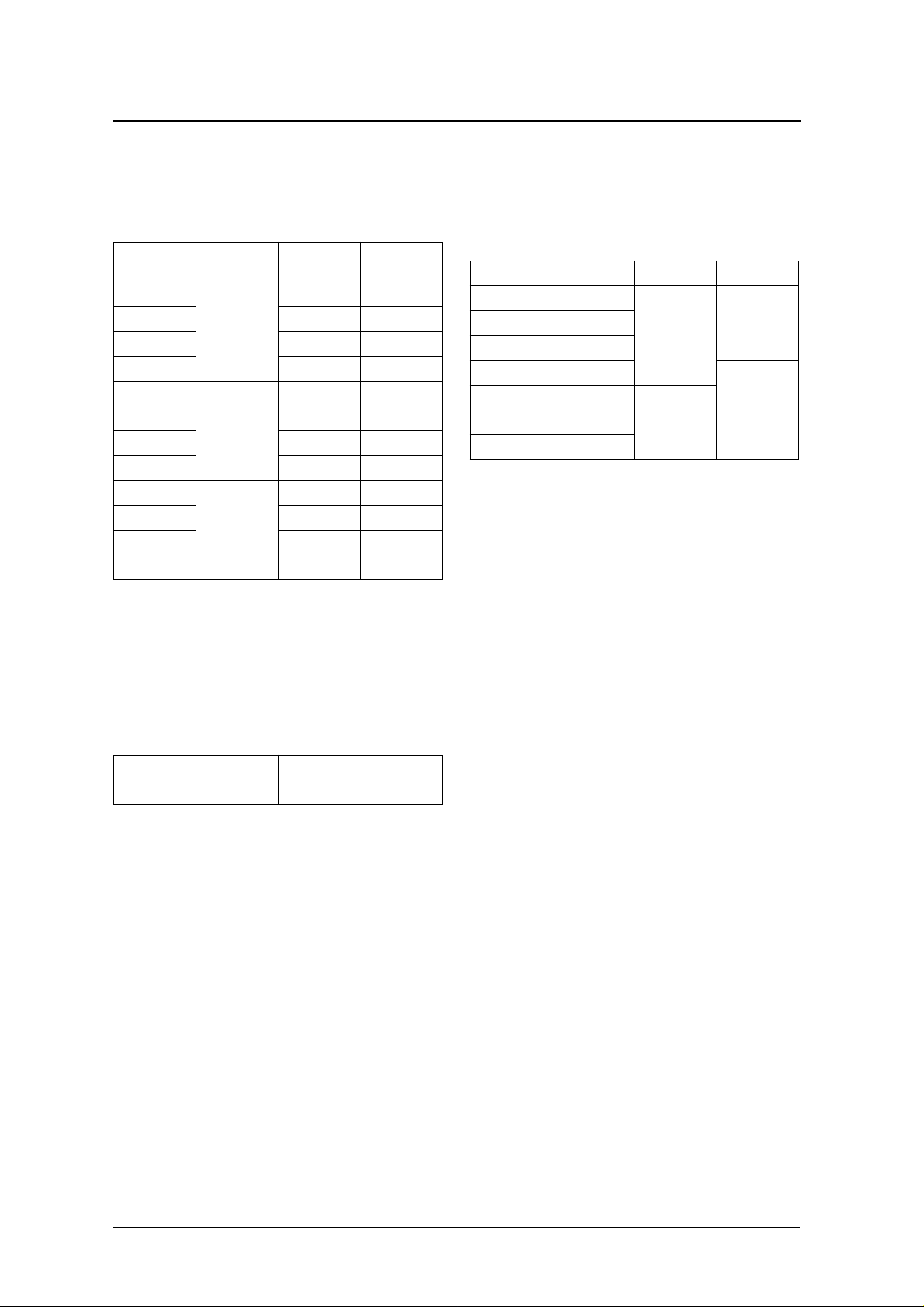
DC Electrical Characteristics
V
= 3.0 to 3.6V, V
DD
Parameter Symbol Condition
Current consumption I
HIGH-level input voltage
L O W -level input voltage
HIGH-level input voltage
L O W -level input voltage
HIGH-level output voltage
L O W-level output voltage
HIGH-level input current
L O W -level input current
Input leakage current
1
1. Pins ICLK and OCLK.
2. Pins DI, BCKI, LRCI, ICKSL, IFM1, IFM2, IWL1, IWL2, DMUTE, MCOM, MDT/FSI1, MCK/FSI2, MLEN/DEEM, OWL1, OWL2, IISN, DITHN,
TST2N, RSTN, THRUN, SLAVE, OCKSL.
3. Pins STATE, LRCO, BCKO, DOUT.
1
2
2
2
1
2
3
3
= 0V, T
SS
= − 40 to 85 ° C
a
DD
V
IH1
V
IL1
V
IH2
V
IL2
V
OH
V
OL
I
IH
I
IL
I
LH
I
LL
Rating
Unit
min typ ma x
No output load – 70 1 00 m A
2.0 – – V
– – 0.8 V
2.0 – – V
– – 0.8 V
I
=
1.0mA V
OH
I
= 1.0mA – – 0.4 V
OL
V
= V
IN
DD
V
= 0V – – 90 µ A
IN
V
= V
IN
DD
V
= 0V – – 1.0 µ A
IN
–0.4 – – V
DD
– – 1.0 µA
– – 1.0 µA
NIPPON PRECISION CIRCUITS—7
Page 8
AC Electrical Characteristics
Input clock (ICLK)
SM5849AF
Parameter Symbol
HIGH-level clock pulsewidth t
L O W -level clock pulsewidth t
Clock pulse cycle t
Output clock (OCLK)
Parameter Symbol
HIGH-level clock pulsewidth t
L O W -level clock pulsewidth t
Clock pulse cycle t
CWH1
CWL1
CY1
CWH2
CWL2
CY2
Condition Rating
System clock m in typ ma x
256fsi 17.5 – –
384fsi 11.7 – –
256fsi 17.5 – –
384fsi 11.7 – –
256fsi 39.0 – 2000
384fsi 26.0 – 1300
Condition Rating
System clock m in typ ma x
256fso 8.7 – –
384fso 5.8 – –
256fso 8.7 – –
384fso 5.8 – –
256fso 19.5 – 1000
384fso 13.0 – 650
Unit
ns
ns
ns
Unit
ns
ns
ns
ICLK and OCLK timing
ICLK
OCLK
t
CWH1,
t
CWH2
t
CY1,
0.5V
DD
t
t
CWL2
CWL1,
t
CY2
NIPPON PRECISION CIRCUITS—8
Page 9

Serial inputs (DI, LRCI, BCKI)
SM5849AF
Parameter Symbol
BCKI HIGH-level pulsewidth t
BCKI LOW-level pulsewidth t
BCKI pulse cycle t
DI setup time t
DI hold time t
Last BCKI rising edge to LRCI edge t
LRCI edge to first BCKI rising edge t
BCKI
t
DS
DI
BCWH1
BCWL1
BCY1
DS
DH
BL1
LB1
Rating
min typ max
50 – – ns
50 – – ns
100 – – ns
50 – – ns
50 – – ns
50 – – ns
50 – – ns
t
t
BCWH1
t
DH
BCY1
t
BCWL1
Unit
0.5V
0.5V
DD
DD
LRCI
t
BL1
t
LB1
0.5V
DD
NIPPON PRECISION CIRCUITS—9
Page 10

Serial inputs (LRCO, BCKO: SLAVE = HIGH)
SM5849AF
Parameter Symbol
BC KO HIGH-level pulsewidth t
B CK O L OW -level pulsewidth t
B C KO pulse cycle t
Last BCKO rising edge to LRCO edge t
LRCO edge to first BCKO rising edge t
BCWH2
BCWL2
BCY2
BL2
LB2
min typ max
39 – – ns
39 – – ns
78 – – ns
39 – – ns
39 – – ns
Rating
Note: BCKO clock inputs exceeding 64 fso cannot be detected, and will cause incorrect operation.
t
t
BCWH2
BCKO 0.5V
t
BL2
LRCO
BCY2
t
BCWL2
t
LB2
Unit
0.5V
DD
DD
NIPPON PRECISION CIRCUITS—10
Page 11

SM5849AF
Microcontroller interface (MCK, MDT, MLEN)
µ
Parameter Symbol
MCK LOW-level pulsewidth t
MCK HIGH-level pulsewidth t
MDT setup time t
MDT hold time t
MLEN LOW-level pulsewidth t
MLEN HIGH-level pulsewidth t
MLEN setup time t
MLEN hold time t
MDT
t
MDS
MCK
t
MCWL t
MCWL
MCWH
MDS
MDH
MLWL
MLWH
MLS
MLH
t
MLS
t
MDH
MCWH
Rating
min typ max
50 – – ns
50 – – ns
50 – – ns
50 – – ns
50 – – ns
50 – – ns
50 – – ns
50 – – ns
t
MLH
Unit
0.5V
0.5V
DD
DD
MLEN
Reset input (RSTN)
Parameter Symbol
First HIGH-level pulsewidth after supply ON t
RSTN pulsewidth t
Note: t
is the system clock input cycle time.
CY
t
= approximately 3.8
RST
V
DD
RSTN
s when t
= 59ns.
CY
t
HRST
HRST
RST
t
MLWL
t
MLWH
Rating
min typ max
– 640 – t
64 – – t
t
RST
0.5V
Unit
CY
CY
DD
NIPPON PRECISION CIRCUITS—11
Page 12

Serial outputs (DOUT, BCKO, LRCO)
SLAVE = LOW, CL = 15pF
SM5849AF
Parameter Symbol Condition
LRCO pulse cycle t
LRCO LOW-level pulsewidth t
LRCO HIGH-level pulsewidth t
B C KO pulse cycle t
B CK O L OW -level pulsewidth t
BC KO HIGH-level pulsewidth t
BC KO to DOUT and LRCO delay
time
SLAVE = HIGH, CL = 15pF
Parameter Symbol Condition
BC KO to DOUT delay time
LOCY
LOWL
LOWH
BOCY
BOWL
BOWH
t
BDH1
t
BDL1
t
BDH2
t
BDL2
Rating
min typ max
Unit
– 1/fso – ns
– 1/2fso – ns
– 1/2fso – ns
OCKSL = LOW – 1/64fso –
OCKSL = HIGH – 1/48fso –
OCKSL = LOW – 1/128fso –
OCKSL = HIGH – 1/96fso –
OCKSL = LOW – 1/128fso –
OCKSL = HIGH – 1/96fso –
BCKO fall to DOUT, LRCO rise – 5 – 2 0 ns
BC K O fall to DOUT, LRCO fall –5 – 20 ns
Rating
min typ max
Unit
B C KO fall to DOUT rise 0 – 5 0 ns
B C K O fall to DOUT fall 0 – 5 0 ns
ns
ns
ns
BCKO
DOUT
LRCO
t
BOCY
t
BOWLtBOWH
t
t
BDH1,
BDL1
t
t
BDH2,
BDL2
t
BDH
t
LOWH
t
LOCY
t
BDL
t
LOWL
0.5V
0.5V
0.5V
DD
DD
DD
NIPPON PRECISION CIRCUITS—12
Page 13

Filter Characteristics
Anti-aliasing filter frequency characteristic
SM5849AF
Filter4
48 to 32kHz
Filter3
44.1 to 32kHz
Frequency [× fsi]
Filter5
0
Filter6
48 to 22.05kHz
-20
-40
-60
-80
Attenuation [dB]
-100
-120
-140
0.15 0.17 0.19 0.22 0.24 0.26 0.28 0.3 0.33 0.35 0.37 0.39 0.41 0.43 0.46 0.48 0.5 0.52 0.54 0.57 0.59 0.61 0.63
48 to 24kHz
Deemphasis filter frequency characteristic
0.00
-2.00
-4.00
Filter2
48 to 44.1kHz
Filter1
Up converter
-6.00
-8.00
Attenuation [dB]
-10.00
-12.00
10 20.23 40.93 82.79 167.5 338.8 685.5 1387 2805 5675 11482 23227
0
-20
-40
-60
-80
Phase Characteristics θ [°]
-100
-120
10 17.3 29.92 51.76 89.54 154.9 267.9 463.4 801.7 1387 2399 4150 7178 12417 21478
Frequency [Hz]
Frequency [Hz]
44.1KHz
48KHz
32KHz
32KHz
44.1KHz
48KHz
NIPPON PRECISION CIRCUITS—13
Page 14

SM5849AF
FUNCTIONAL DESCRIPTION
Input Data Interface (DI, LRCI, BCKI, IFM1, IFM2, IWL1, IWL2)
Table 1. Input data format (IFM1, IFM2, IWL1, IWL2)
Mode IFM1 IFM2 IWL1 IWL2 Word length Data position
1LOWLOW
2 L OW HIGH Right justified LSB first
L O W L O W 16 bits
3 HIGH L OW Left justified MSB first
4 HIGH HIGH IIS MSB first
5LOWLOW
6 L OW HIGH Right justified LSB first
HIGH LOW 20 bits
7 HIGH L OW Left justified MSB first
8 HIGH HIGH IIS MSB first
9LOWLOW
10 L OW HIGH Right justified LSB first
LOW or HIGH HIGH 24 bits
11 HIGH LOW Left justifie d MSB first
12 HIGH HIGH IIS MSB first
Right justified MSB first
Right justified MSB first
Right justified MSB first
Attenuator and Deemphasis Selection
The attenuator is set using the microcontroller interface. When the attenuator is used, deemphasis settings also need to be set using the microcontroller
interface. The microcontroller interface comprises
MDT, MCK and MLEN, and is used to transfer all
input serial data.
Data
sequence
Table 2. Attenuator and deemphasis function select
Function set method
Function
Deemphasis ON/OFF DEEM FDEEM
Deemphasis frequency (fsi) select FSI1, FSI2 FFSI1, FFSI2
Attenuator data set N/A (no attenuation) 11 bits (B0 to B10)
Test mode select N/A (test mode 1) FTST1, FTST2
MCON should not be switched after a power-ON
reset.
External pins
(MCOM = LOW)
When MCOM is LOW, the logic levels on FSI1,
FSI2 and DEEM select the device function.
Microcontroller interface
(MCOM = HIGH)
When MCOM is HIGH, serial data received on
MDT , MCK and MLEN sets the attenuation data and
control flag data.
NIPPON PRECISION CIRCUITS—14
Page 15

SM5849AF
,
,
,
,
,
,,,,
,
,
,
Microcontroller Interface (MCOM, MDT, MCK, MLEN)
When MCOM is HIGH, the microcontroller interface is active, comprising MDT (data), MCK (clock)
and MLEN (latch enable clock) interface pins.
Input data on MDT is synchronized to the MCK
clock. Data is read into the input stage shift register
on the rising edge of MCK. Accordingly, the input
data should change on the falling edge of MCK.
Input data enters an internal SIPO (serial-to-parallel
converter register), and then the parallel data is
MLEN
1 12
MCK
,,,,,,,
MDT
,,,
,,,
D1
D2 D3 D4 D5 D6 D7 D8 D9 D10 D11 D12
MSB LSB
B0 B1 B2 B3 B4 B5 B6 B7 B8 B9 B10"L"
Figure 1. Attenuation data format (D1 = LOW)
latched into the mode register on the rising edge of
the latch enable clock MLEN.
The mode register addressed is determined by bit D1
of the 12 data bits before MLEN goes HIGH. If this
bit is LOW, then the data is read into the attenuation
data register as shown in figure 1. If this bit is HIGH,
then the data is read into the mode flag register as
shown in figure 2. The function of each bit in the
mode flag register is described in table 3.
,,,
,,,
MLEN
MCK
MDT
,,,,,,
,,,
1 12
D2 D3 D4 D5 D6 D7 D8 D9 D10 D11 D12
D1
"L" "L" "L" "L" FTST1 FTST2 FRATE F12DB FFSI1 FFSI2 FDEEM"H"
Figure 2. Mode flag data format (D1 = HIGH)
,,
,,
NIPPON PRECISION CIRCUITS—15
Page 16

Table 3. Mode flag description
SM5849AF
D1 Bit Mode flag
D2 to D7 (Not used) Test mode select
D 8 F RATE Input/output ra te
D9 F12DB Attenuator
HIGH
D10 FFSI1
D11 FFSI2
D12 FDEEM
Mode function select
Parameter LOW/HIGH Select
IC test mode flags.
Not used for normal operation.
D2 to D7 should be set LOW.
Set the input/output sample rate ratio for each
output sample
Set the input/output sample rate ratio with high
accuracy every 2048 output samples
fsi select
FFSI2 FFSI1 fsi
LOW LOW
LOW HIGH
HIGH LOW 48.0kHz
HIGH HIGH 32.0kHz
Deemphasis filter fs
select 1
Deemphasis filter fs
select 2
Deemphasis control
ON/OFF
HIGH
LOW
HIGH +12dB gain shift
L O W No gain shift (normal operation)
HIGH Deemphasis filter ON
LOW Deemphasis filter OFF
Reset
mode
LOW
LOW
LOW
LOW
44.1kHz
LOW
LOW
Deemphasis (DEEM, FSI1, FSI2 pins or FDEEM, FFSI1, FFSI2 flags)
The digital deemphasis filter is an IIR filter with variable coefficients to faithfully reproduce the gain and
phase characteristics of analog deemphasis filters.
The filter coefficients are selected by FSI1 (or FFSI1
flag) and FSI2 (or FFSI2 flag) to correspond to the
sampling frequencies fs = 44.1, 48.0 and 32.0kHz.
Table 4. Deemphasis ON/OFF
DEEM
(MCOM = LOW)
HIGH ON
LOW OFF
FDEEM
(MCOM = HIGH)
Table 5. Deemphasis fs select (FSI1, FSI2 pins or
FFSI1, FFSI2 flags)
MCOM = LOW (MCOM = HIGH)
FSI1 (FFSI1) FSI2 (FFSI2)
LOW LOW
HIGH LOW
LOW HIGH 48.0kHz
HIGH HIGH 32.0kHz
Deemphasis
fs
44.1kHz
NIPPON PRECISION CIRCUITS—16
Page 17

Attenuation (MDT, MCK, MLEN)
,
,
,
,
,
SM5849AF
The digital attenuator coefficients are read in as
serial data on the microcontroller interface. Data on
MDT is read into the internal shift register on the rising edge of MCK, and then 12 bits are latched internally on the rising edge of MLEN.
MLEN
1 12
MCK
,,,,,,,
MDT
,,,
,,,
D1
D2 D3 D4 D5 D6 D7 D8 D9 D10 D11 D12
MSB LSB
B0 B1 B2 B3 B4 B5 B6 B7 B8 B9 B10"L"
Figure 3. Attenuation data format (microcontroller interface)
Although the attenuation data comprises 11 bits,
only 1025 levels are valid as given by the following.
10
DATT ai2
=
∑
i 0=
10 i–()
×
The gain of the attenuator for values of DATT from
001H to 400H are given by the following equations.
Note that when the F12DB flag is HIGH, the gain is
shifted by a fixed +12.0412dB.
When the leading bit is 0 (D1 = LOW), the following
11 bits are read into the attenuation register and used
as an unsigned integer in MSB first format. See figure 3.
,,,
,,,
DATT
Gain 20
--------------- -
log× [dB]=
1024
when F12DB = LOW
DATT
20
when F12DB = HIGH
--------------- -
log× [dB]=
256
−∞
−∞
−
−
−
−
After a system reset initialization, DATT is set to
400H and the F12DB flag is LOW, corresponding to
0dB gain. (The F12DB flag is described in table 3.)
Table 6. Attenuator settings
D1
LOW
Attenuation data
400H (to 7FFH) 0 1.0 12.041 4.0
F12DB = LOW (default) F12DB = HIGH
DATT
000H
001H
↓↓↓↓↓
100H
↓↓↓↓↓
3FFH
Gain (dB) Linear expression Gain (dB) Linear expression
0.0
60.206 1/1024
12.041 256/1024 0.0 256/256
0.0085 1023/1024 12.032 1023/256
48.165 1/256
0.0
NIPPON PRECISION CIRCUITS—17
Page 18

Attenuator operation
SM5849AF
A change in the attenuation data DATT causes the
gain to change smoothly from its previous value
towards the new setting. The new attenuation data is
stored in the attenuation data register and the current
attenuation level is stored in a temporary register.
Consequently, if a new attenuation level is read in
before the previously set level is reached, the gain
Level 1
0 dB
Gain
Level 2
— ∞
∆t
Figure 4. Attenuator operation example
Mute (DMUTE)
Direct mute
changes smoothly from the current value towards the
latest setting as shown in figure 4.
The attenuation counter output changes, and hence
the gain changes, by 1 step every output sample. The
time taken to reduce the gain from 0dB (or 12dB) to
dB is (1024/fso), which corresponds to approxi-
mately 23.2ms when fso = 44.1kHz.
Level 5
Level 3
Level 4
Time
Table 7. DMUTE operation ON/OFF
DMUT
E
LOW
HIGH 0 data is output from the next output word (mute ON)
Nor mal data is output from the next output word (mute
OFF)
Function
Other mute operations
The direct mute function is also invoked at the following times.
When the reset input (RSTN) changes.
■
When the fs setting changes, for deemphasis,
■
using either FSI1, FSI2 inputs or FFSI1, FFSI2
flags.
When the ICKSL, IFM1, or IFM2 setting changes.
■
When the ICLK input system clock stops.
■
Table 8. Other mute operations
Input Function
RSTN = LOW
RSTN = HIGH
FSI1, FSI2 input settings
changed (MCOM = LOW).
FFSI1, FFSI2 input settings
changed (MCOM = HIGH)
ICKSL, IFM1, IFM2 input
settings change.
ICLK input system clock stops.
ICLK input system clock
restarts.
0 data is output from the next
output word (mute ON)
No rmal data is output from the
3073rd output word (mute OFF)
0 data is output from the next
output word (mute ON).
No rmal data is output from the
3073rd output word (mute OFF)
0 data is output from the next
output word (mute ON)
No rmal data is output from the
3073rd output word (mute OFF)
−∞
NIPPON PRECISION CIRCUITS—18
Page 19

Internal Operating Status (STATE)
SM5849AF
Internally, all functions are performed on 24-bit
serial data, and the conversion rate and filter type are
selected accordingly. The output format is 24-bit
left-justified.
Table 9. Status data description
Output bit position Content
(Output data cycle/input data cycle)
Ex.
1 to 20
21 Not used.
22 DA2
23 DA1
24 DA0
1st 20th
00.111111111111011111 ⇒ 1.0 times
01.111111111111011111 ⇒ 2.0 times (1/2 conversion rate ratio)
00.011111111111011111 ⇒ 0.5 times (2.0 conversion rate ratio)
Selected filter type
129
DA2 DA 1 D A 0 Filter type C o n ve rsion frequency (example)
0 0 0 1 Up converter
0 0 1 2 48 to 44.1kHz
0 1 0 3 44.1 to 32kHz
0 1 1 4 48 to 32kHz
1 0 0 5 96 to 48kHz, 48 to 24kHz
1 0 1 6 96 to 44.1kHz, 48 to 22.05kHz
Note that when THRUN is LOW, LRCO and BCKO
are not guaranteed to be synchronized to the STATE
output.
Input System Clock (ICLK, ICKSL)
−
×
The input system clock can be set to run at either
256fsi or 384fsi, where fsi is the input frequency on
LRCI.
Note that ICLK and LRCI should be divided from a
common clock source or PLL to maintain synchronism.
Output System Clock (OCLK, OCKSL)
The output system clock can be set to run at either
256fso or 384fso, where fso is the output frequency
on LRCO. In through mode, OCLK and OCKSL
have no function and are not used.
Note that even in slave mode, a suitable clock must
be input on OCLK. A malfunction prevention circuit
uses this clock so that operation continues when the
ICLK stops.
Table 10. ICKSL and input system clock
ICKSL ICLK system clock rate
HIGH 384fsi
L OW 256fsi
Table 11. SLAVE, OCKSL and output system clock
SLAVE OCKSL OCLK system clock rate
LOW
HIGH
HIGH 384fso
LO W 256fso
Not used
NIPPON PRECISION CIRCUITS—19
Page 20

SM5849AF
Output Data Interface and Output Clock Selection (LRCO, BCKO, DOUT, SLAVE)
Table 12. Output mode description
THRUN SLAVE
LOW Master mode
HIGH
HIGH Slave mode
LOW
1. The number of BCKO input clock cycles should not exceed 64 per word. Correct operation is not guaranteed beyond these limits.
Mode Description LRCO, BCKO state
Output word clock (LRCO) and output bit clock
(B CKO) are divided from OCLK.
Output word clock (LRCO) and output bit clock
(BCKO) are supplied externally.
Through mode
Output word clock (LRCO), output bit clock (BCKO)
and output data (DOUT) are the same as LRCI,
BCKI and DI, respectively. DMUTE is valid.
Function
Output Format Control (OWL1, OWL2, IISN)
The output is in MSB-first, 2s-complement, L/R
alternating, bit serial format with a continuous bit
clock.
Inputs Output format
Mode
IISN OWL 2 OW L 1
1
2 LOW HIGH 20 bits
3 HIGH LOW 24 bits
4 HIGH HIGH 24 bits
5
7 HIGH
L O W L O W 16 bits
HIGH
L O W L O W 16 bits
LOW
Word
length
×
24 bits
IIS
selection
Normal
(non IIS)
IIS6 LOW HIGH 20 bits
Data
position
Right
justified
Left
justified
Outputs
1
Inputs
Outputs
×
Output Timing Calculation
The output timing is controlled to maintain the
desired ratio between the output data cycle and the
input data cycle.
Output round-off processing
The internal processor data length and output data
length are different, making output data round-off
processing necessary. The SM5849AF supports
selectable normal round-off processing and trigonometric function dither round-off processing
*
TPDF: Triangular Probability Density Function
*
.
DITHN Output round-off processing
HIGH Normal round-off
L O W Dither round-off
NIPPON PRECISION CIRCUITS—20
Page 21

Filter Characteristic Selection
SM5849AF
Conversion rates from 0.45 to 2.2 times are supported using the following 6 filter types.
The ratio between the output sample rate and input
sample rate is measured automatically and the most
suitable filter type for this ratio is selected automatically.
Table 13. fs ratio and filter selection
Filter
mode
fs ratio (fso/fsi) Selects range
1 1.0 to 2.2 ≥ 0.969697 Up converter
2 0.91875
3 0.72562
4 0.66667
5 0.50000
6 0.459375 ≤ 0.492308
0.864865 to
0.969697
0.711111 to
0.864865
0.627451 to
0.711111
0.492308 to
0.627451
Co n version
frequency
(example)
48.0 to 44.1kHz
44.1 to 32.0kHz
48 to 32kHz
48 to 24kHz,
96 to 48kHz
48 to 22.05kHz,
96 to 44.1kHz
System Reset (RSTN)
When the selected fs conversion ratio and the actual
sample rate conversion ratio do not coincide, the following phenomenon occur.
Table 14. Mismatch condition and response
Condition
Actual sample rate conversion
ratio is low er than the selected
filter conversion ratio
Actual sample rate conversion
ratio is higher than the selected
filter conversion ratio
1. An output noise may be generated if the fs conversion r atio changes at
a rate greater 0.119%/sec.
1
Response
The audio band high-pass
develops aliasing noise.
The audio band high-pass is cut
off.
At power-ON, all de vice functions must be reset. The
device is reset by applying a LOW-level pulse on
RSTN. At system reset, the internal arithmetic operation, output timing counter and internal flag register
operation are synchronized on the next LRCI rising
edge. Note that all flags are set to their defaults (all
LOW).
Through Mode (THRUN)
Table 15. Through mode function description
THRUN Mode Description
LOW Through mode
HIGH Normal mode Sample rate converter operation
Direct connections are made: LRCI
to LRCO, BCKI to BCKO , and DI to
DOUT. DMUTE is valid.
Synchronizing Internal Arithmetic Timing
The clock on LRCI should pass through 1 cycle for
every 384 (ICKSL = HIGH) or 256 (ICKSL = LOW)
ICLK clock cycles to maintain correct internal arithmetic sequence. If the number of ICLK cycles is different, increases or decreases, or any jitter is present,
device operation could be affected.
There is a fixed-value tolerance within which the
internal sequence and LRCI clock timing are not
adversely affected.
A power-ON reset signal can be applied from an
external microcontroller. For systems where ICLK
and LRCI are stable at power ON, initialization can
be performed by connecting a 0.001µF capacitor
between RSTN and VSS. Otherwise, a capacitor
value should be chosen such that RSTN does not go
HIGH until after LRCI and ICLK have stabilized.
Table 16. ICLK and clock tolerance
ICKSL Allowa b le clock variation
HIGH (384fs mode) +8 to −6 cycles
LO W (256fs mode) +4 to −3 cycles
Whenever the allowable tolerance is exceeded, the
internal sequence start-up may be delayed or fail.
When this occurs, there is a possibility that a click
noise will be generated.
NIPPON PRECISION CIRCUITS—21
Page 22

SM5849AF
TIMING DIAGRAMS
Input Timing Examples (DI, BCKI, LRCI)
Audio data input timing (right-justified 16-bit word, IFM1 = L, IFM2 = L, IWL1 = L, IWL2 = L)
LRCI(fsi)
1242548
BCKI(48fsi)
LSB MSBMSB LSB
DI
Audio data input timing (right-justified 24-bit word, IFM1 = L, IFM2 = L, IWL1 = H, IWL2 = H)
LRCI(fsi)
1 24
BCKI(48fsi)
DI
87654321 87654321 2423222120191817161514131211109
16151413121110987654321 16151413121110987654321
25 48
LSBMSBMSB LSB
2423222120191817161514131211109
Audio data input timing (left-justified 20-bit word, IFM1 = H, IFM2 = L, IWL1 = H, IWL2 = L)
LRCI(fsi)
1 24
25 48
BCKI(48fsi)
LSB MSBMSB LSB
DI
87654321 87654321 20191817161514131211109
20191817161514131211109
All data bits after the LSB (20th bit) are ignored. Note that more than 20 BCKI cycles are required.
Audio data input timing (IIS-format 24-bit word, IFM1 = H, IFM2 = H, IWL1 = L, IWL2 = H)
LRCI(fsi)
1 32 33
BCKI(64fsi)
LSBMSB
DI
242322212019181716151413121110987654321
MSB LSB
87654321 2423222120191817161514131211109
Audio data input timing (right-justified 24-bit word, LSB first,
IFM1 = H, IFM2 = H, IWL1 = L, IWL2 = H)
64
LRCI(fsi)
BCKI(64fsi)
1 32
DI
64
MSB LSBLSB MSB
24232221201918171615141312111093387654321 87654321 2423222120191817161514131211109
NIPPON PRECISION CIRCUITS—22
Page 23

SM5849AF
Output Timing Examples (DOUT, BCKO, LRCO)
Audio data output timing (right-justified 16-bit word, IISN = H, OWL1 = L, OWL2 = L)
LRCO(fso)
1242548
BCKO(48fso)
LSB MSBMSB LSB
DOUT
Audio data output timing (right-justified 24-bit word, IISN = H, OWL1 = L, OWL2 = H)
LRCO(fso)
1 24
BCKO(48fso)
DOUT
87654321 87654321 2423222120191817161514131211109
16151413121110987654321 16151413121110987654321
25 48
LSBMSBMSB LSB
2423222120191817161514131211109
Audio data output timing (left-justified 24-bit word, IISN = H, OWL1 = H, OWL2 = H)
LRCO(fso)
BCKO(64fso)
1 32
LSB MSBMSB LSB
DOUT
24232221201918171615141312111093387654321 87654321 2423222120191817161514131211109
Audio data output timing (IIS-format 24-bit word, IISN = L, OWL1 = L, OWL2 = H)
LRCO(fso)
1 32 33
BCKO(64fso)
MSB LSB
87654321 2423222120191817161514131211109
DOUT
LSBMSB
242322212019181716151413121110987654321
Audio data output timing (right-justified 24-bit word, IISN = H, OWL1 = L, OWL2 = H)
LRCO(fso)
BCKO(64fso)
DOUT
1 32
LSB MSBMSB LSB
24232221201918171615141312111093387654321 87654321 2423222120191817161514131211109
64
64
64
NIPPON PRECISION CIRCUITS—23
Page 24

State Data Output Timing
State data output timing
IISN = H
LRCO(fso)
1 32
BCKO(64fso)
STATE
IISN = L
LRCO(fso)
1 32
BCKO(64fso)
STATE
SM5849AF
64
LSBMSB
24232221201918171615141312111093387654321
64
LSBMSB
24232221201918171615141312111093387654321
Delay Time
t
is the time when the serial input data read in
INPUT
is completed (on the rising edge of LRCI). t
is the time when the serial output data read out is
1/fs
Serial data input
t
input
1/fso
t
INPUT
t
OUTPUT
OUTPUT
55 ± 5
— t
INPUT
completed (on the rising edge of LRCO). The delay
between input and output is given by t
= (55 ± 5)/fsi.
PUT
Serial data output
t
output
OUTPUT
− t
IN-
t
OUTPUT
NIPPON PRECISION CIRCUITS—24
Page 25

TYPICAL APPLICATIONS
Input Interface Circuit
Digital audio interface receiver (CS8414)
SM5849AF
MCK
FSYNC
SCK
SDATA
DIR
CS8414
Co/F0
SEL
CS12/FCK
M3
M2
M1
M0
5V
Output Interface Circuit
Digital audio interface receiver (CS8404)
24.576MHz (256fso) 3.3V
Level Shifter
(5V to 3.3V)
External Clock
(256fsi)
3.3V
12.288MHz (128fso) 5V
ICLK
LRCI
BCKI
DI
MLEN/DEEM
ICKSL
MCOM
IFM1
IFM2
IWL1
IWL2
SM5849AF
OCLK MCK
SM5849AF
LRCO
BCKO
DOUT
OCKSL
OWL1
OWL2
IISN
THRUN
SLAVE
3.3V
3.3V
Level Shifter
(3.3V to 5V)
5V
FSYNC
SCK
SDATA
PRO
TRNPT/FC1
M2
M1
M0
DIT
CS8404
NIPPON PRECISION CIRCUITS—25
Page 26

SM5849AF
NIPPON PRECISION CIRCUITS INC. reserves the right to make changes to the products described in this data sheet in order to
improve the design or performance and to supply the best possible products. Nippon Precision Circuits Inc. assumes no responsibility for
the use of any circuits shown in this data sheet, conveys no license under any patent or other rights, and makes no claim that the circuits
are free from patent infringement. Applications for any devices shown in this data sheet are for illustration only and Nippon Precision
Circuits Inc. makes no claim or warranty that such applications will be suitable for the use specified without further testing or modification.
The products described in this data sheet are not intended to use for the apparatus which influence human lives due to the failure or
malfunction of the products. Customers are requested to comply with applicable laws and regulations in effect now and hereinafter,
including compliance with export controls on the distribution or dissemination of the products. Customers shall not export, directly or
indirectly, any products without first obtaining required licenses and approvals from appropriate government agencies.
NIPPON PRECISION CIRCUITS INC.
4-3, Fukuzumi 2-chome
Koto-ku, To kyo 135-8430, Japan
NIPPON PRECISION CIRCUITS INC.
Telephone: 03-3642-6661
Facsimile: 03-3642-6698
NC9914BE 2000.06
NIPPON PRECISION CIRCUITS—26
 Loading...