Page 1

SM5847AF
NIPPON PRECISION CIRCUITS INC.
High-fidelity Digital Audio, Multi-function Digital Filter
OVERVIEW
The SM5847AF is a 4/8-times oversampling (interpolation), 2-channel, linear-phase FIR, multi-function digital filter for digital audio reproduction
equipment. It features independent left and rightchannel digital deemphasis filters and soft muting
function.
The input/output interface supports input data in
16/18/20/24-bit words, and output data in
18/20/22/24-bit words in either 4-times or 8-times
oversampling selectable output mode.
FEATURES
■
Left/right-channel (2-channel processing)
■
4-times/8-times oversampling (interpolation)
• 8-times interpolation filter
- 3-stage linear-phase FIR configuration
1st stage (fs to 2fs): 169-tap
2nd stage (2fs to 4fs): 29-tap
3rd stage (4fs to 8fs): 17-tap
- ≤ ±0.00002 dB passband ripple (0 to
0.4535fs)
- ≥ 117 dB stopband attenuation (0.5465fs to
7.4535fs)
• 4-times interpolation filter
- 2-stage linear-phase FIR configuration
1st stage (fs to 2fs): 169-tap
2nd stage (2fs to 4fs): 29-tap
- ≤ ±0.00002 dB passband ripple (0 to
0.4535fs)
- ≥ 116 dB stopband attenuation (0.5465fs to
3.4535fs)
■
Digital deemphasis
• IIR filter configuration
• fs = 32kHz, 44.1kHz, 48kHz
• 2-channel independent ON/OFF control
■
26 × 24-bit parallel multiplier/32-bit accumulator
■
Overflow limiter
■
Soft muting
• 2-channel independent ON/OFF control
■
Input data format
The internal system clock operates at either 192fs or
256fs selectable speed (where fs is the audio sampling frequency). Plus, the divide-by 1, 2, or 4
counter settings means that external clocks of 768fs/
384fs/192fs (192fs input) and 1024fs/512fs/256fs
(256fs input) are supported.
The SM5847AF operates from a single 3 to 5 V supply, and is available in 44-pin QFP packages.
• 2s complement, MSB first
• 3 selectable formats
- LR alternating, 16/18/20/24-bit serial, rightjustified data
- LR alternating, 24-bit serial, left-justified
data
- LR simultaneous, 24-bit serial, left-justified
data
■
Output data format
• 2s complement, MSB first, LR simultaneous
• 18/20/22/24-bit serial
• BCKO burst (NPC format)
■
Dither round-off processing
• Dither round-off ON/OFF selectable
■
25-bit internal data word length
■
Internal system clock
• 192fs/256fs selectable
• Maximum operating frequency
192fs mode: 37 MHz max (5 V)
20.7 MHz max (3 V)
256fs mode: 27.6 MHz max (5 V)
25 MHz max (3 V)
■
Jitter-free function
• Jitter-free/Sync mode selectable
■
Crystal oscillator circuit built-in
■
3 to 5 V supply
■
44-pin plastic QFP
■
CMOS process
ORDERING INFORMATION
De vice Pack ag e
SM5847AF 44-pin QFP
NIPPON PRECISION CIRCUITS—1
Page 2
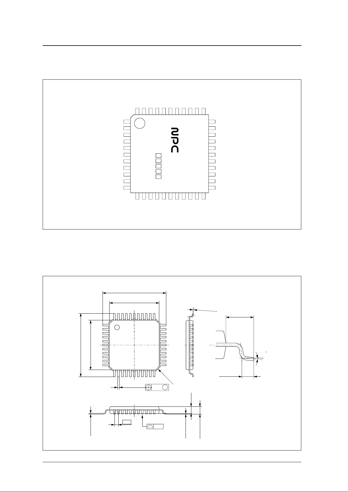
PINOUT
(T op V iew)
SM5847AF
OMD
DOR
DOL
WCKO
BCKO
VSS
VSSAC
VDDAC
VDD
DG
NC
PACKAGE DIMENSIONS
(Unit: mm)
44-pin plastic QFP
MUTEL
DITHN
MUTER
42
43
44
1
2
3
4
5
6
7
8
9
10
11
1213141516171819202122
VSS
CKO
VDD
FSEL2
41
SM58 4
7AF
XTO
FSEL1
40
XTI
VSS
39
VSS
VDD
38
VDD
DEMPL
DEMPR
36
37
LRCI
DI/INF2N
CKDV2
CKDV1
34
35
NC
BCKI
33
RSTN
32
SYNCN
31
OW2N
30
OW1N
29
VDD
28
VSS
27
IW2N/DIR
26
IW1N/DIL
25
INF1N
24
CKSLN
23
NC
0.30
+
−
12.80
+
10.00 0.30
+
0.17 0.05
+
12.80
0.30
−
+
10.00 0.30
−
0.17
+
0.05
−
(1.40)
−
0 to 10
0.35
4
−
C 0.7
+
0.10
−
0.20 M
0.60
+
0.20
−
(1.40)
−
0.80
0.15
+
−
0.15 0.05
0.20
+
−
1.50 0.10
NIPPON PRECISION CIRCUITS—2
Page 3
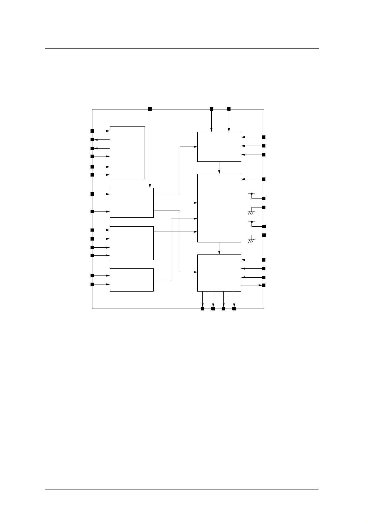
BLOCK DIAGRAM
SM5847AF
XTI
XTO
CKO
CKSLN
CKDV1
CKDV2
SYNCN
RSTN
DEMPL
DEMPR
FSEL1
FSEL2
MUTEL
MUTER
System
Clock
Timing
Controller
Deemphasis
Controller
Mute
Controller
LRCI
BCKI
Input Data
Interface
Filter and
Attenuation
Arithmetic
Block
Output Data
Interface
Block
DI/INF2N
IW1N/DIL
IW2N/DIR
INF1N
DITHN
VDD
VSS
VDDAC
VSSAC
OMD
OW1N
OW2N
DG
BCKO
DOL
WCKO
DOR
NIPPON PRECISION CIRCUITS—3
Page 4
SM5847AF
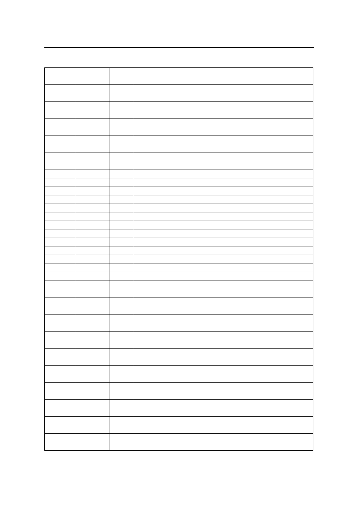
PIN DESCRIPTION
Number Name I/O Description
1
1 OMD Ip
2 DOR O
3 DOL O
4 WCKO O
5 BCKO O
6 VS S – Ground
7 VSSAC – Ground
8 V D D AC – Supply voltage
9 V D D – Supply voltage
10 D G O
11 N C – No internal connection (must be open)
12 CKO O
13 VS S – Ground
14 V D D – Supply voltage
15 X TO O Oscillator output
16 XTI I Oscillator input/master clock input
17 VS S – Ground
18 V D D – Supply voltage
19 LRCI I
20 DI/INF2N I
21 BCKI I
22 N C – No internal connection (must be open)
23 N C – No internal connection (must be open)
24 CKSLN Ip
25 INF1N Ip
26 IW1N/DIL Ip
27 IW2N/DIR Ip
28 VS S – Ground
29 V D D – Supply voltage
30 OW1N Ip
31 OW2N Ip
32 SYNCN Ip
33 RSTN Ip
34 CKDV1 Ip
35 CKDV2 Ip
36 DEMPR Ip
37 DEMPL Ip
38 V D D – Supply voltage
39 VS S – Ground
40 FSEL1 Ip
41 FSEL2 Ip
42 MUTEL Ip
43 MUTER Ip
44 DITHN Ip
1. Schmitt input, TTL level
2. TTL level
Ip = Pull-up input
Output data rate (4fs/8fs) select pin
2
Right-channel data output
2
Left-channel data output
2
Word clock output
2
Bit clock output
2
Deglitched signal output
2
Master clock output
1
Input data sample rate (fs) clock input
1
Data input/input format select pin 2
1
Bit clock input
2
Master clock frequency (192fs/256fs) select pin
2
Input format select pin 1
1
Input data word length select pin 1/left-channel data input
1
Input data word length select pin 2/right-channel data input
2
Output data word length select pin 1
2
Output data word length select pin 2
2
Sync mode select pin
1
Reset input
1
Internal system clock frequency divider set pin 1
1
Internal system clock frequency divider set pin 2
1
Right-channel deemphasis ON/OFF pin
1
Left-channel deemphasis ON/OFF pin
1
Deemphasis filter sample rate (fs) select pin 1
1
Deemphasis filter sample rate (fs) select pin 2
1
Left-channel mute ON/OFF pin
1
Right-channel mute ON/OFF pin
1
Output data dither ON/OFF pin
NIPPON PRECISION CIRCUITS—4
Page 5
−
+
( °
−
−
°
≤
°
°
−
° C
−
−
−
−
−
−
−
SM5847AF
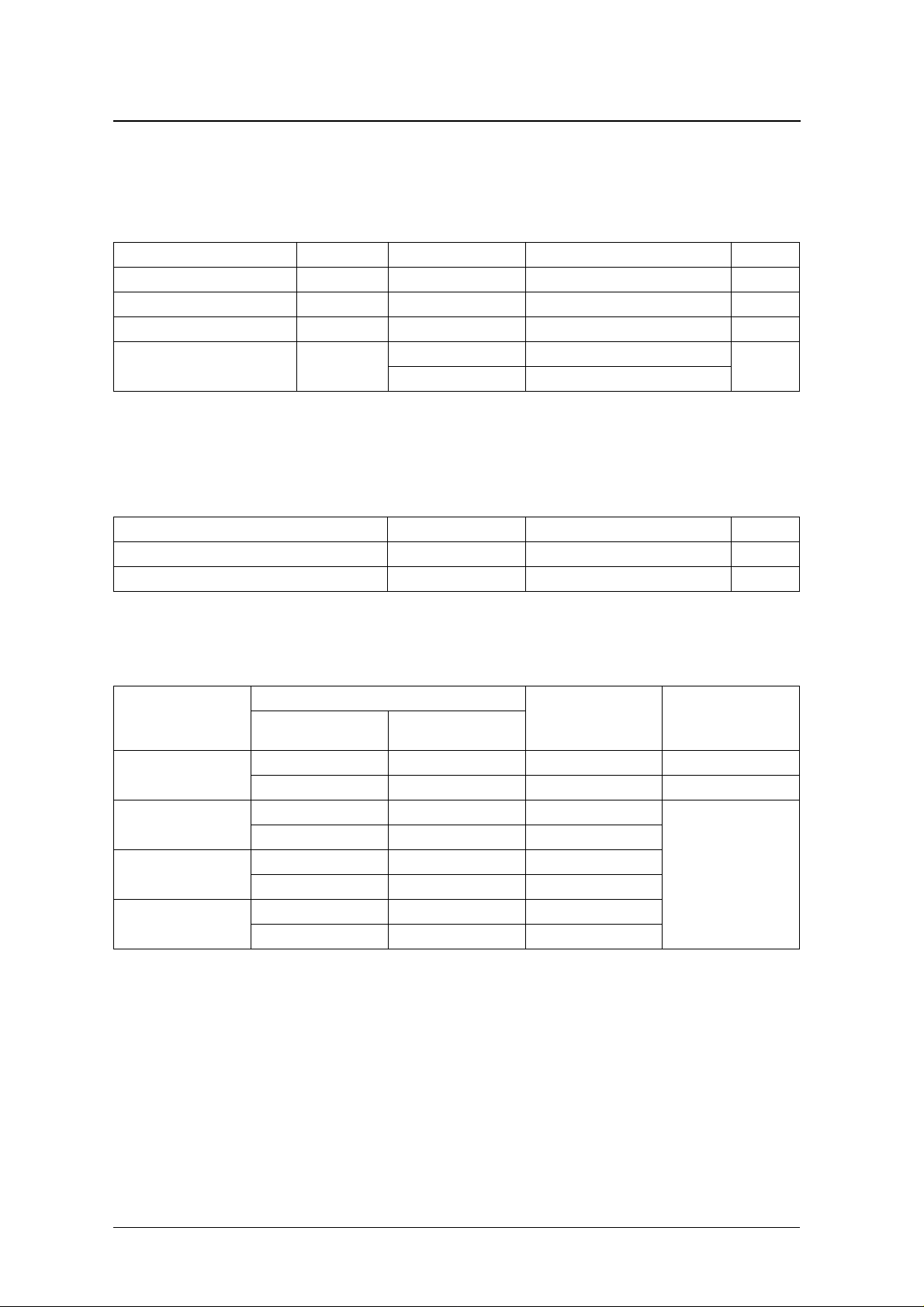
SPECIFICATIONS
Absolute Maximum Ratings
V
= V
SS
Supply voltage range
Input voltage range V
Storage temperature range T
Po w er dissipation P
1. Supply lines for VDD and VDD AC, and ground lines for VSS and VSSAC, should be connected on the printed circuit board to prevent device breakdo wn due to potential difference when the power is applied.
= 0 V, V
SSAC
Parameter Symbol Condition Rating Unit
1
DD
= V
DDAC
V
DD
, V
DDAC
I
stg
D
70
C 900
≤ 85
C 700
0.3 to 6.5 V
V
SS
0.3 to V
55 to 125
0.3 V
DD
C
mW
Recommended Operating Conditions
V
= V
SS
Supply voltage range
Operating temperature range T
1. The minimum required operating voltage and consequent operating temperature vary with the maximum operating frequency and sampling mode
selected, as shown in the following table.
V
= V
SS
Sampling frequency
1. Mode with internal frequency divider ratio set to 1 (CKDV1 = CK DV2 = L OW) .
2. 96 kHz + 12.5% variable pitch
3. 48 kHz + 15% variable pitch
SSAC
SSAC
fs (kHz)
192
2
108
96
3
55.2
= 0 V, V
1
= 0 V, V
= V
DD
DDAC
Parameter Symbol Rating Unit
V
DD
, V
DD
DDAC
a
= V
DDAC
Internal system clock
1
Mode
192fs 37 4.75 (5.0
256fs Not guaranteed Not guaranteed Not guaranteed
192fs 20.7 3.00 (3.3 −
256fs 27.6 4.50 (5.0
192fs 18.5 3.00 (3.3
256fs 25 3.00 (3.3
192fs 10.6 3.00 (3.3 −
256fs 14.2 3.00 (3.3
Maximum operating
frequency (MHz)
Minimum supply voltage
3.00 to 5.25 V
40 to 85
V
, V
DDAC
10%)
10%)
10%)
10%)
10%)
10%)
(V)
5%)
DD
Operating temperature
T
C)
a
40 to 70
40 to 85
NIPPON PRECISION CIRCUITS—5
Page 6
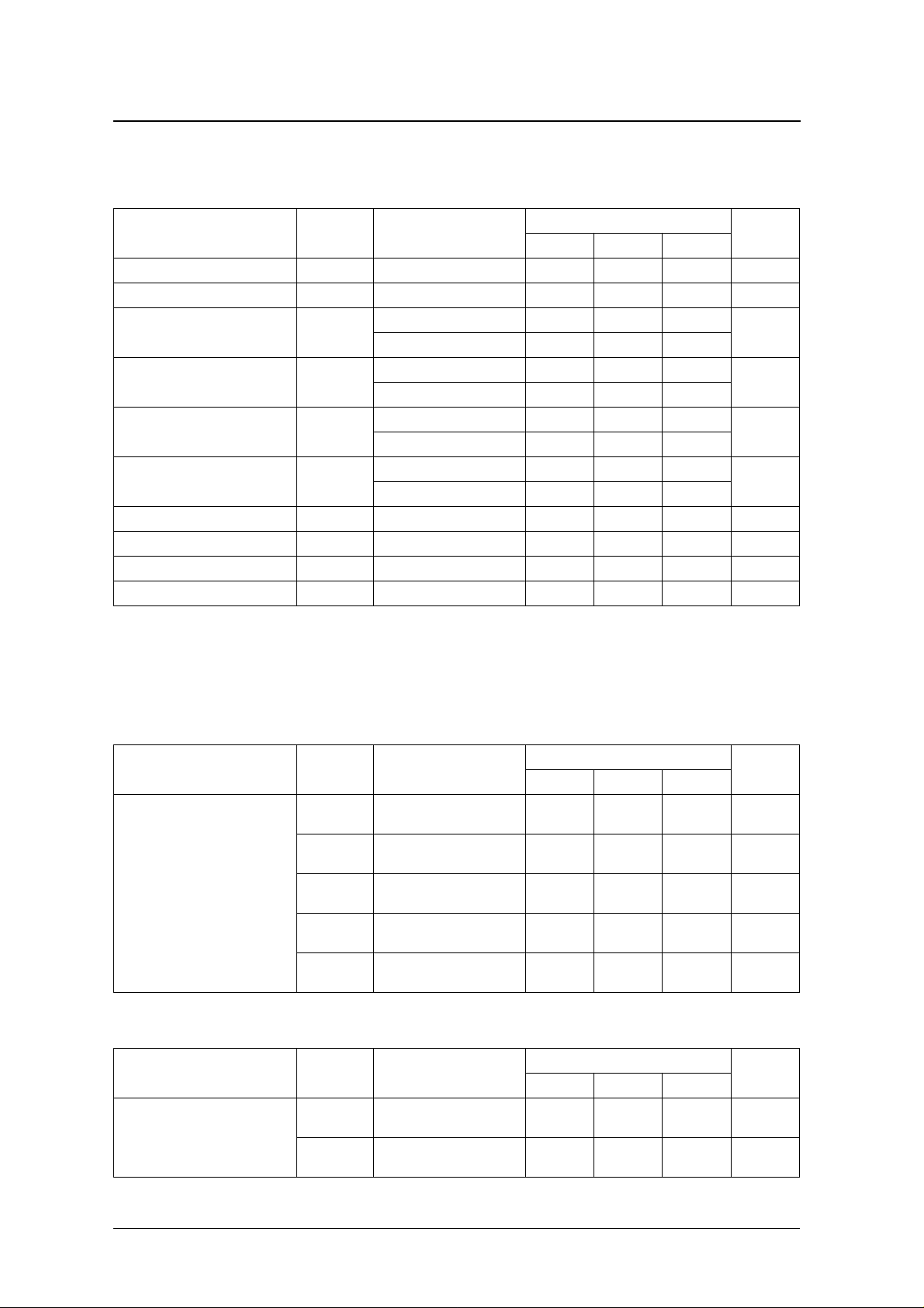
DC Electrical Characteristics
V
DD
= V
= 3.00 to 5.25 V, V
DDAC
SS
= V
SSAC
SM5847AF
= 0 V, T
= − 40 to 85 ° C
a
Parameter Symbol Condition
HIGH-level input voltage
HIGH-level input voltage
HIGH-level input voltage
L O W -level input voltage
L O W -level input voltage
L O W -level input voltage
Input leakage current
Input current
3,4
1
2,4
3
1
2,4
3
1,2
HIGH-level output voltage
L O W-level output voltage
min typ max
V
IH1
V
IH2
V
= V
V
IH3
V
IL1
DD
V
DD
V
DD
V
DD
VDD = V
V
IL2
VDD = V
VDD = V
V
IL3
I
IL1
I
IL2
5
5
V
OH
V
OL
VDD = V
VIN = 0 to 5.25 V
VIN = 0 V
IOH = −4 mA 2.4 – – V
IOL = 4 mA – – 0.4 V
= 4.75 to 5.25 V 2.4 – –
DDAC
= V
= 3.00 to 4.75 V 2.0 – –
DDAC
= V
= 4.75 to 5.25 V – – 0.3V
DDAC
= V
= 3.00 to 4.75 V – – 0.2V
DDAC
= 4.75 to 5.25 V – – 0.8
DDAC
= 3.00 to 4.75 V – – 0.2V
DDAC
= 4.75 to 5.25 V – – 0.8
DDAC
= 3.00 to 4.75 V – – 0.2V
DDAC
0.7V
DD
––V
2.0 – – V
DD
DD
DD
DD
−
10 – 10 µA
−
10
−
50
−
120 µA
Unit
V
V
V
V
1. Pin XTI
2. Pins LRCI, DI/INF2N, BCKI
3. Pins IW1N/DIL, IW2N/DIR
4. Pins OMD, CKSLN, INF1N, OW1N, OW2N, SYNCN, RSTN, CKDV1, CKDV2, DEMPR, DEMPL, FSEL1, FSEL2, MUTEL, MUTER, DITHN
5. Pins DOR, DOL, W C K O , BCKO, DG, CKO
Rating
V
DD
= V
= 4.75 to 5.25 V, V
DDAC
Parameter Symbol Condition
Current consumption
V
DD
= V
= 3.00 to 3.60 V, V
DDAC
Parameter Symbol Condition
Current consumption
SS
I
DD1
I
DD2
I
DD3
I
DD4
I
DD5
SS
I
DD6
I
DD7
= V
SSAC
= 0 V, T
192fs, XTI = 2 7 ns (37 MHz),
fs = 192 kHz,Ta = −40 to 70 °C
256fs, XTI = 4 0 ns (25 MHz),
fs = 9 6 kH z
384fs, XTI = 2 7 ns (37 MHz),
fs = 96 kHz, estimated value
192fs, XTI = 54 ns (18.5 MHz),
fs = 96 kHz, estimated value
384fs, XTI = 54 ns (18.5 MHz),
fs = 48 kHz, estimated value
= V
SSAC
= 0 V, T
256fs, XTI = 81 ns (12.3 MHz),
fs = 48 kHz, estimated value
384fs, XTI = 54 ns (18.5 MHz),
fs = 48 kHz, estimated value
= − 40 to 85 ° C, XTI = external input, no output load
a
Rating
Unit
min typ max
– – 166 m A
– – 115 m A
– – 105 m A
––95mA
––65mA
= − 40 to 85 ° C, XTI = external input, no output load
a
Rating
Unit
min typ max
––27mA
––28mA
NIPPON PRECISION CIRCUITS—6
Page 7
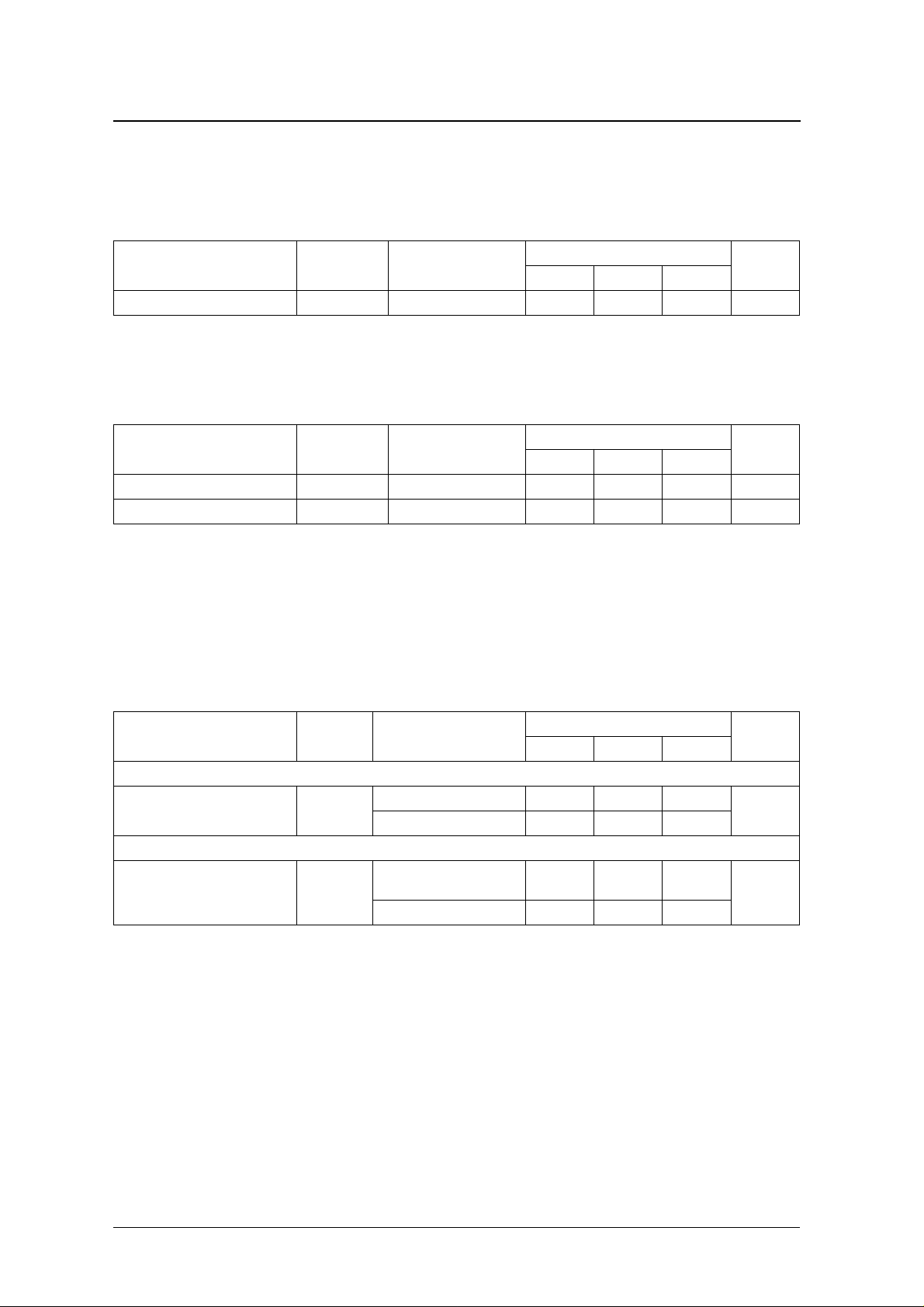
AC Electrical Characteristics
Crystal oscillator (XTI, XTO)
SM5847AF
VDD = V
Oscillator frequency
1. External circuit components should be matched for the crystal oscillator element used.
= 3.00 to 5.25 V, VSS = V
DDAC
Parameter Symbol Condition
1
f
OSC
= 0 V, Ta = −40 to 85 °C
SSAC
Rating
Unit
min typ max
– – 50 MHz
External clock input (XTI)
VDD = V
Master clock frequency f
Master clock duty 1/2VDD thresholds 40 – 60 %
= 3.00 to 5.25 V, VSS = V
DDAC
Parameter Symbol Condition
XTI
= 0 V, Ta = −40 to 85 °C
SSAC
Rating
Unit
min typ max
– – 60 MHz
Internal system clock
The crystal oscillator frequency or external clock input master clock frequency ratings are described in the preceding tables, but it is the internal system clock frequency rating, set by the internal frequency divider
(CKDV1, CKDV2), that must be satisfied. The master clock frequency is a multiple of the sampling frequency
fs.
CKDV1 = CKDV2 = LOW (internal system clock frequency = XTI input frequency),
VSS = V
256fs (CKSLN = LOW, CKDV1 = LOW, CKDV2 = LOW)
System clock frequency f
192fs (CKSLN = HIGH, CKDV1 = LOW , CKDV2 = LOW)
System clock frequency f
= 0 V, Ta = −40 to 85 °C
SSAC
Parameter Symbol Condition
SYS1
SYS2
VDD = V
VDD = V
VDD = V
Ta = −40 to 70 °C
VDD = V
= 4.50 to 5.25 V 0.256 – 27.6
DDAC
= 3.00 to 5.25 V 0.256 – 2 5
DDAC
= 4.75 to 5.25 V,
DDAC
= 3.00 to 5.25 V 0.384 – 20.7
DDAC
Rating
min typ max
0.384 – 3 7
Unit
MHz
MHz
NIPPON PRECISION CIRCUITS—7
Page 8
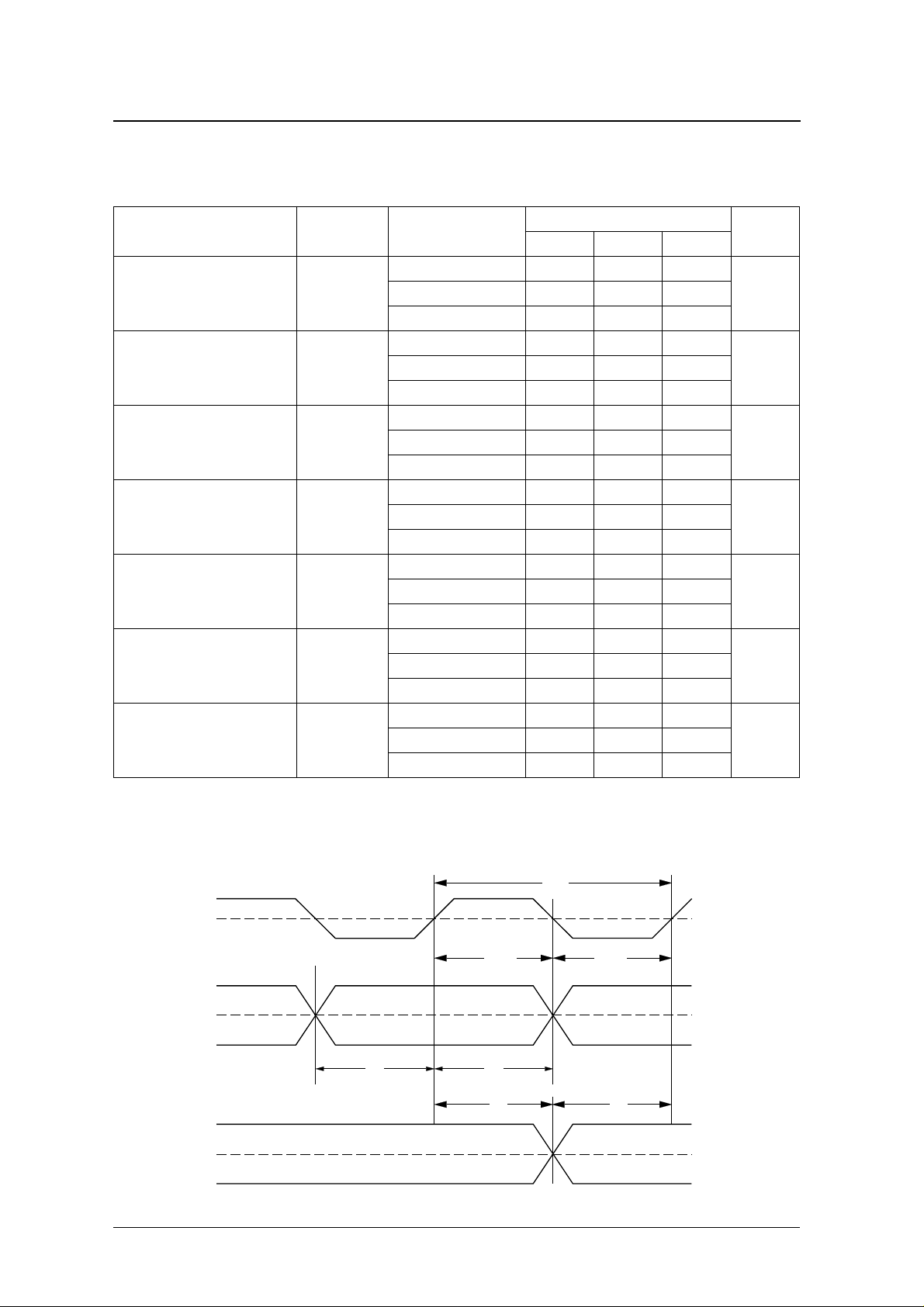
SM5847AF
Serial input timing (BCKI, LRCI, DI/INF2N, IW1N/DIL, IW2N/DIR)
VSS = V
BCKI pulse cycle t
BCKI HIGH-level pulsewidth t
BCKI LOW-level pulsewidth t
DI, DIL, DIR setup time t
DI, DIL, DIR hold time t
Last BCKI rising edge to LRCI edge t
LRCI edge to first BCKI rising edge t
= 0 V, Ta = −40 to 85 °C
SSAC
Parameter Symbol Condition
IBCY
BCWH
BCWL
DS
DH
BL
LB
Rating
Unit
min typ max
Note 1 55 – –
nsNote 2 80 – –
Note 3 100 – –
Note 1 25 – –
nsNote 2 35 – –
Note 3 45 – –
Note 1 25 – –
nsNote 2 35 – –
Note 3 45 – –
Note 1 10 – –
nsNote 2 20 – –
Note 3 30 – –
Note 1 10 – –
nsNote 2 20 – –
Note 3 30 – –
Note 1 10 – –
nsNote 2 20 – –
Note 3 30 – –
Note 1 10 – –
nsNote 2 20 – –
Note 3 30 – –
1. CKSLN = HIGH (192fs), VDD = V
2. CKSLN = LOW (256fs), VDD = V
CKSLN = HIGH (192fs), VDD = V
3. CKSLN = LOW (256fs), V
DD
= V
BCKI
DI
DIL
DIR
LRCI
= 4.75 to 5.25 V, Ta = −40 to 70 °C
DDAC
= 4.50 to 5.25 V
DDAC
= 3.00 to 4.75 V
DDAC
= 3.00 to 4.50 V
DDAC
tDS
tIBCY
tBCWH tBCWL
tDH
tBL
NIPPON PRECISION CIRCUITS—8
1.5V
1.5V
tLB
1.5V
Page 9
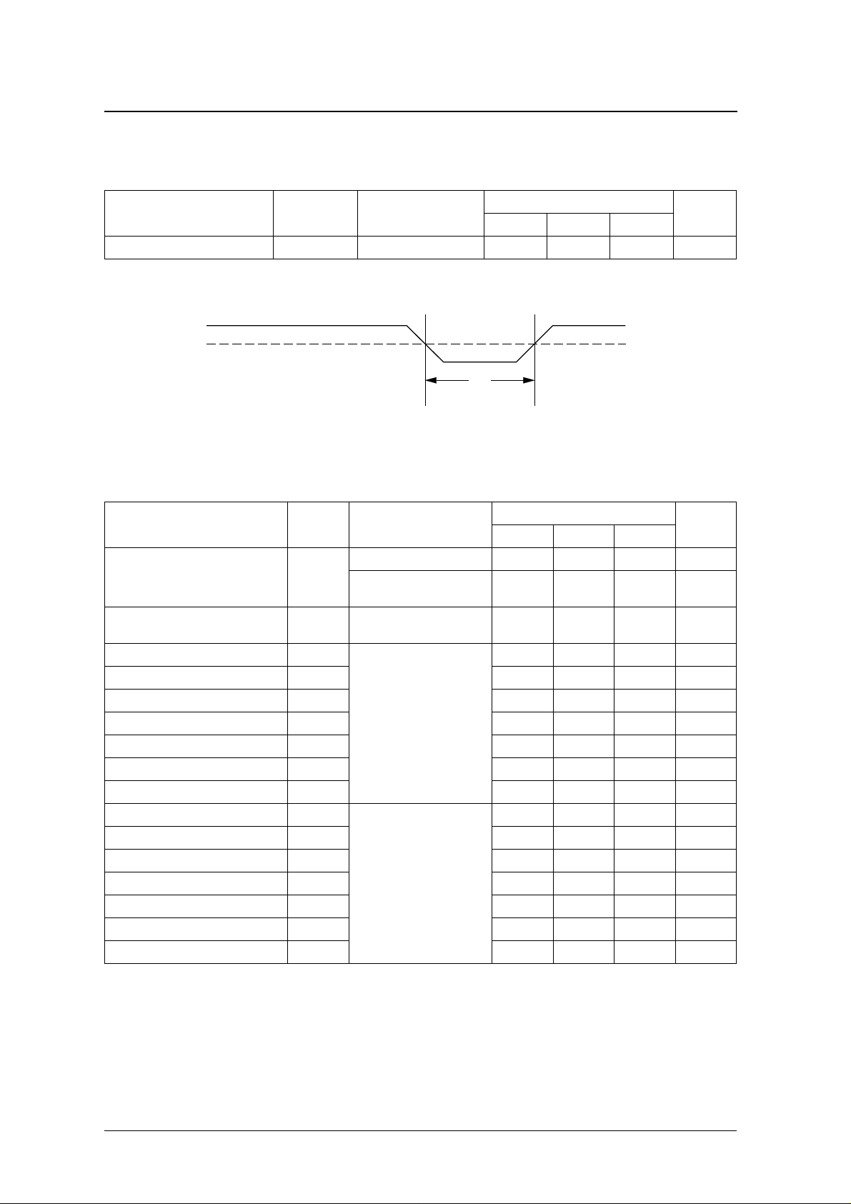
Reset timing (RSTN)
SM5847AF
VDD = V
= 3.00 to 5.25 V, VSS = V
DDAC
= 0 V, Ta = −40 to 85 °C
SSAC
Parameter Symbol Condition
RSTN LOW-level reset pulsewidth t
1. t
is equal to 1/f
MCK
XTI
or 1/f
. For example, t
OSC
RST
= 54 ns when f
RST
= 37 MHz.
XTI
RSTN
Output timing (CKO, BCKO, WCKO, DOL, DOR, DG)
VDD = V
XTI falling edge to CKO falling edge delay t
BCKO falling edge to WCKO, DOL, DOR,
DG delay
B C K O r ising edge to W CK O falling edge t
W CK O falling edge to BCKO rising edge t
BC KO per iod t
BC KO HIGH-level pulsewidth t
B CK O L OW -level pulsewidth t
DOL, DOR setup time t
DOL, DOR hold time t
B C K O r ising edge to W CK O falling edge t
W CK O falling edge to BCKO rising edge t
BC KO per iod t
BC KO HIGH-level pulsewidth t
B CK O L OW -level pulsewidth t
DOL, DOR setup time t
DOL, DOR hold time t
= 4.75 to 5.25 V, VSS = V
DDAC
= 0 V, Ta = −40 to 70 °C, CL = 50 pF
SSAC
Parameter Symbol Condition
XTO
VDD = V
DDAC
Ta = −40 to 85 °C
t
BDO
WOH
Output mode: 8fs
WOS
OBCY
OBCH
OBCL
ODS
ODH
WOH
WOS
OBCY
OBCH
OBCL
ODS
ODH
OMD = HIGH (fs = 192 kHz)
External clock input:
XTI = 27 ns (37 MHz),
CKSLN = HIGH (192fs)
Divider ratio: 1
CK DV1 = CKDV2 = LOW
Output data length: 24 bits
OW1N = OW2N = LOW
Output mode: 4fs
OMD = LOW (fs = 192 kHz)
External clock input:
XTI = 27 ns (37 MHz),
CKSLN = HIGH (192fs)
Divider ratio: 1
CK DV1 = CKDV2 = LOW
Output data length: 24 bits
OW1N = OW2N = LOW
= 3.00 to 5.25 V,
1
min
2t
MCK
tRST
min typ max
4–9ns
4–11ns
−
4– 2ns
8––ns
8––ns
27 – – ns
7––ns
7––ns
7––ns
7––ns
17 – – ns
17 – – ns
54 – – ns
18 – – ns
18 – – ns
18 – – ns
18 – – ns
Rating
typ ma x
Unit
––ns
1.5V
Rating
Unit
NIPPON PRECISION CIRCUITS—9
Page 10

SM5847AF
VDD = V
= 4.50 to 5.25 V, VSS = V
DDAC
Parameter Symbol Condition
BC KO HIGH-level pulsewidth t
B CK O L OW -level pulsewidth t
DOL, DOR setup time t
DOL, DOR hold time t
BC KO HIGH-level pulsewidth t
B CK O L OW -level pulsewidth t
DOL, DOR setup time t
DOL, DOR hold time t
XTI
CKO
OBCH
OBCL
ODS
ODH
OBCH
OBCL
ODS
ODH
= 0 V, Ta = −40 to 85 °C, CL = 50 pF
SSAC
External clock input: XTI = 36 ns
(27.6 MHz), CKSLN = LO W
(256fs), fs = 108 kH z
Divider ratio: 1
CK DV1 = CKDV2 = LOW
Output mode: 8fs, OMD = HIGH
External clock input: XTI = 36 ns
(27.6 MHz), CKSLN = LO W
(256fs), fs = 108 kH z
Divider ratio: 1
CK DV1 = CKDV2 = LOW
Output mode: 4fs, OMD = LOW
tXTO
Rating
Unit
min typ max
10 – – ns
10 – – ns
11 – – ns
11 – – ns
26 – – ns
26 – – ns
27 – – ns
27 – – ns
1.5V
1.5V
WCKO
BCKO
DOL
DOR
BCKO
WCKO
DOL
DOR
DG
tOBCH
tOBCY
tOBCL
tODS
1.5V
1.5V
tBDO
1.5V
tWOH tWOS
1.5V
1.5V
tODH
NIPPON PRECISION CIRCUITS—10
Page 11

Filter Characteristics
8-times interpolation filter
Parameter Rating
Passband 0 to 0.4535fs
Stopband 0.5465fs to 7.4535fs
Passband ripple ≤ ±0.00002 dB
Stopband attenuation ≥ 117 dB
Group delay Constant
8fs filter response with deemphasis OFF
0
20
40
(dB)
60
80
Attenuation
100
SM5847AF
120
140
0.0 1.0 2.0 4.0 5.0 6.0 7.0 8.0
3.0
Frequency (× fs)
8fs filter band transition response with deemphasis OFF
-0.00008
(dB)
-0.00004
0.00000
0.00004
Attenuation
0.00008
0.000 0.125 0.250 0.375 0.500
Frequency (× fs)
8fs filter passband response with deemphasis OFF
0
20
40
60
80
100
Attenuation (dB)
120
140
0.440 0.465 0.490 0.515 0.540 0.565 0.590 0.615 0.640
Frequency
(× fs)
NIPPON PRECISION CIRCUITS—11
Page 12

4-times interpolation filter
Parameter Rating
Passband 0 to 0.4535fs
Stopband 0.5465fs to 3.4535fs
Passband ripple ≤ ±0.00002 dB
Stopband attenuation ≥ 116 dB
Group delay Constant
4fs filter response with deemphasis OFF
0
20
40
60
80
100
Attenuation (dB)
120
140
0.0
0.5 1.0 1.5 2.0 2.5 3.0 3.5 4.0
SM5847AF
Frequency (× fs)
4fs filter band transition response with deemphasis OFF
-0.00008
-0.00004
0.00000
0.00004
0.00008
Attenuation (dB)
0.000 0.125 0.250 0.375 0.500
Frequency (× fs)
4fs filter passband response with deemphasis OFF
0
20
40
60
80
100
120
Attenuation (dB)
140
0.440 0.465 0.490 0.515
0.540
Frequency (× fs)
0.565 0.590 0.615 0.640
NIPPON PRECISION CIRCUITS—12
Page 13

Deemphasis filter
SM5847AF
Parameter
Sampling frequency (fs)
32 kHz 44.1 kHz 48 kHz
Passband bandwidth (kHz) 0 to 14.5 0 to 20.0 0 to 21.7
Attenuation ≤ ±0.01 dB
D eviation from ideal character istic
Phase,
θ
0 to 1.5
°
Passband response with deemphasis ON
0
2
4
6
8
Attenuation (dB)
10
10 100 1k 10k 20 50 200 500 2k 5k 20k
Attenuation
32kHz
Phase
32kHz
44.1kHz
48kHz
44.1kHz
48kHz
0
-20
-40
-60
[Hz]
Phase (degrees)
Frequency (Hz)
NIPPON PRECISION CIRCUITS—13
Page 14

FUNCTIONAL DESCRIPTION
Oversampling (Interpolation)
SM5847AF
The interpolation arithmetic block is comprised of 3
cascaded, 2-times FIR interpolation filters, as shown
in figure 1. The input signal is sampled at rate fs, and
then either 4-times or 8-times oversampling data is
Input
fs
2-times interpolator
1st FIR
169-tap
2fs
2-times interpolator
2nd FIR 29-tap
4fs
Deemphasis OFF
Deemphasis ON
output. Sampling noise in the 0.5465fs to 3.4535fs
(4fs output) or 0.5465fs to 7.4535fs (8fs output)
region is removed.
Deemphasis IIR filter
4fs
Soft mute
4fs
2 -times interpolator
3rd FIR 17-tap
8fs
4fs
Output
Figure 1. Arithmetic operating block
NIPPON PRECISION CIRCUITS—14
Page 15

SM5847AF
Digital Deemphasis (DEMPL, DEMPR, FSEL1, FSEL2)
Most deemphasis filters are constructed using analog
circuit techniques. Here, an IIR filter is employed to
faithfully reproduce the gain and phase characteristics of standard analog deemphasis filters, corresponding to analog 50µs/15µs frequency
characteristics. Three sets of filter coefficients for the
three fs = 32/44.1/48 kHz sampling frequencies are
supported. Deemphasis for other values of fs are not
supported.
Deemphasis ON/OFF (DEMPL, DEMPR)
Deemphasis for the left and right-channel can be
controlled independently.
Table 1. Deemphasis control
DEMPL DEMPR Deemphasis
LOW
HIGH
×
×
×
×
LO W Right-channel OFF
HIGH Right-channel ON
Left-channel OFF
Left-channel ON
Filter coefficient select (FSEL1, FSEL2)
Table 2. Deemphasis filter coefficient select
FSEL1 FSEL2 Sampling frequency (fs)
LO W LOW 44.1 kHz
LOW HIGH 48 kHz
HIGH LOW Prohibited mode
HIGH HIGH 32 kHz
Soft Muting (MUTEL, MUTER)
The muting function controls the muting of left and
right-channel independently. Input data continues to
be accepted even when mute is operating.
Mute ON/OFF
When MUTEL (MUTER) goes HIGH, the attenuation changes smoothly from 0 to −∞ dB. Similarly,
when MUTEL (MUTER) goes LOW, muting is
released and the attenuation changes smoothly from
−∞ to 0 dB. This operation is termed soft muting.
Soft muting takes an interval of approximately
512/fs, or about 11.6 ms when fs = 44.1 kHz.
Table 3. Mute control
MUTEL MUTER Soft muting
LOW
HIGH
×
×
×
×
LO W Right-channel OFF
HIGH Right-channel ON
Left-channel OFF
Left-channel ON
Mute operation at reset
When RSTN goes LOW, the DOL and DOR outputs
are immediately muted to −∞ dB. When RSTN goes
HIGH, reset is released and the outputs are immediately set to 0 dB attenuation.
Note that even when either MUTEL or MUTER or
both are HIGH, the reset operation takes precedence.
NIPPON PRECISION CIRCUITS—15
Page 16

Analog Output Click Noise
,
SM5847AF
Under the following conditions, a click noise may be
output from the DAC (digital-to-analog converter)
connected to the SM5847AF.
■ When a system reset on RSTN occurs
■ When the internal system clock mode, set by
CKSLN, CKDV1, and CKDV2, is switched
■ When the deemphasis mode, set by DEMPL,
DEMPR, FSEL1, and FSEL2, is switched
DI/INF2N,
IW1N/DIL, IW2N/DIR
MUTEL/MUTER
RSTN
Gain
External DAC
analog output
(full scale signal)
,,,,,,,,,,,,,,,,,,,,,,,,,,,,,,,,,,,,,,,,,,
H
512/fs
FS: full scale
512/fs
■ When the audio data input mode, set by INF1N,
DI/INF2N, IW1N/DIL, and IW2N/DIR, is
switched
■ When the SYNCN jitter-free mode switch timing
exceeds the internal timing delay limit
An external muting circuit connected to the analog
output may be required to eliminate this noise.
Normal operation
LH L
soft mutesoft mute
LLHH
resetreset
0dB
−∞
+FS
zero
-FS
click noise
Figure 2. Soft muting/reset operation
NIPPON PRECISION CIRCUITS—16
Page 17

SM5847AF
Internal System Clock (XTI, XTO, CKO, CKSLN, CKDV1, CKDV2)
The SM5847AF supports two system clock frequencies selected by CKSLN, 192fs and 256fs, where fs
is the sampling frequency.
The master clock can be provided either by a crystal
oscillator connected between XTI and XTO, or by an
external master clock input on XTI. Note that the
feedback resistor required by the oscillator option is
not built-in. External components should be selected
to match the crystal oscillator element. Note also that
XTO must be left open (floating) for the external
master clock input option.
Note that even though it is necessary that the master
clock and LRCI clock (sampling frequency fs) be in
sync, it is not necessary that they be exactly in-phase
(see jitter-free mode description).
The SM5847AF features independent divide-by 1, 2,
or 4counter, selected by CKDV1 and CKDV2. This
provides the 192fs or 256fs system clock with the
necessary divider ratios to support master clocks
with frequencies of 768fs, 384fs, 192fs, 1024fs,
512fs or 256fs.
Normal sampling frequencies 32 kHz, 44.1 kHz,
48 kHz, 88.2 kHz, 96 kHz, 176.4 kHz and 192 kHz
are supported. However, some combinations of sampling frequency and master clock frequency are not
supported, as follows.
■ 768fs and 1024fs at 88.2 and 96 kHz
■ 768fs, 384fs, 1024fs, 512fs, and 256fs at
176.4 kHz
■ 768fs, 384fs, 1024fs, 512fs and 256fs at 192 kHz
Note also that the internal crystal oscillator circuit
cannot operate at frequencies ≥ 50 MHz. The master
clock input on XTI is output on CKO.
Table 4. Internal system clock select
CKSLN System clock
LO W 256fs
HIGH 192fs
Table 5. System clock frequency divider ratio select
CKDV1 CKDV2
LO W L OW 1 192fs, 256fs
LOW HIGH – Prohibited mode
HIGH LOW 4 768fs, 1024fs
HIGH HIGH 2 384fs,512fs
16 15 12
XTI XTO
R1
XTAL
C1 C2
Divider
ratio
Divider
CKO
Master Clock
Buffer output
Master clock
SM5847AF
Figure 3. Crystal oscillator connection
Master clock stop operation
The master clock is input after power is applied.
But if, after the XTI and LRCI clocks are input and
power-ON reset occurs with all-zero input audio
data, the master clock input on XTI is held either
HIGH or LOW level, operation effectively stops.
Note also that a reset signal is not accepted when the
master clock and LRCI clock stop.
16 15 12
XTI XTO
External Clock
XTO : open
Figure 4. External clock connection
NIPPON PRECISION CIRCUITS—17
Divider
SM5847AF
CKO
Master Clock
Buffer output
Page 18

Table 6. Master clock frequency example
SM5847AF
XTI system clock frequency (MHz)
Sampling
frequency
fs (kHz)
32 6.144 12.288 24.576 8.192 16.384 32.768
44.1 8.4627 16.9344 33.8688 11.2896 22.5792 45.1584
48 9.216 18.432 36.864 12.288 24.576 49.152
88.2 16.9344 33.8688 Not guaranteed
96 18.432 36.864 Not guaranteed 24.576 49.152 Not guaranteed
176.4 33.8688 Not guaranteed Not guaranteed Not guaranteed Not guaranteed Not guaranteed
192 36.864 Not guaranteed Not guaranteed1Not guaranteed Not guaranteed Not guaranteed
1. R efer to the AC characteristics system clock ratings.
CKDV1 CKDV2 CKDV1 CKDV2 CKDV1 CKDV2 CKDV1 CKDV2 CKDV1 CKDV2 CKDV1 CKDV2
LOW LOW HIGH HIGH HIGH LOW LOW LOW HIGH HIGH HIGH LOW
192fs 384fs 768fs 256fs 512fs 1024fs
CKSLN = HIGH (192fs) CKSLN = LOW (256fs)
1
22.5792 45.1584 Not guaranteed
System Reset (RSTN)
During normal device operation, reset signals are not
required. However, the SM5847AF must be reset
under the following conditions.
■ At power-ON
■ When the LRCI clock and internal operation tim-
ing need to be resynchronized in jitter-free mode.
■ After the LRCI or XTI clocks, or both, stop and
are subsequently started.
The system is reset by applying a LOW-level pulse
on RSTN.
When RSTN is LOW, the DOL and DOR outputs are
tied LOW, muting the output signal to an attenuation
level of −∞.
After system reset, when RSTN goes HIGH, the
arithmetic and output timing counters are reset on
the first LRCI start edge, assuming that the XTI and
LRCI input clocks have already stabilized. The LRCI
start edge is determined by the state of INF1N and
INF2N. When INF1N is LOW or when both INF1N
and INF2N are HIGH, the start edge is the rising
edge. When INF1N is HIGH and INF2N is LOW, the
start edge is the falling edge.
RSTN=L
zero
Internal reset
WCKO
DOL/DOR
RSTN
LRCI
OMD=H
8fs
OMD=L
4fs
Figure 5. System reset timing and output muting (INF1N = LOW or INF1N = INF2N = HIGH)
NIPPON PRECISION CIRCUITS—18
Page 19

SM5847AF
Audio Data Input (INF1N, DI/INF2N, IW1N/DIL, IW2N/DIR, BCKI, LRCI)
The input data format and input pin functions are
selected by the state of INF1N and INF2N. When
INF1N is LOW, the inputs are left and right-channel
data inputs, and when INF1N is HIGH, the
DI/INF2N input is an input format select pin, and
DIL and DIR are the audio data inputs.
Input data format select
Table 7. Input settings and functions
INF1N DI/INF2N Input for ma t
LOW
LOW
HIGH LOW LR alternating, left-justified data
HIGH HIGH LR simultaneous2, left-justified data
1. Alternating left-channel and r ight-channel data input on a single input DI.
2. Si m ultaneous left-channel and right-channel data input on two inputs, DIL and DIR, respectively.
−
LR alternating1, right-justified data
−
Input data word length
The input data word length is selected by the state of
IW1N and IW2N when INF1N is LOW. 20-bit is
selected when INF1N is HIGH.
Table 8. Input data word length select
INF1N IW1N/DIL IW2N/DIR Input word length
Pin function selection
DI/INF2N IW1N/DIL IW2N/DIR
DI IW1N IW2N
INF2N DIL DIR
L O W L O W 24 bits
Jitter-free Function (SYNCN)
The arithmetic circuit and output control timing is
derived from the system clock, and is therefore independent of the input LRCI and BCKI clocks.
Accordingly, any jitter in the data input clock (LRCI
and BCKI) does not cause jitter in the output.
Generally, the internal timing is synchronized to the
LRCI input timing after a system reset release, when
RSTN goes from LOW to HIGH, on the first LRCI
clock start edge. If the input timing and LRCI start
edge timing subsequently drift, the input timing is
automatically resynchronized when the timing error
exceeds a certain value. There are 2 timing error values at which resynchronization occurs, selected by
the state of SYNCN.
Jitter-free mode (SYNCN = HIGH)
LOW
HIGH L OW 20 bits
LOW HIGH 18 bits
HIGH HIGH 16 bits
HIGH – – 24 bits
resynchronized and all functions continue to operate
normally.
Sync mode (SYNCN = LOW)
When SYNCN is LOW, the timing error value is ±1
× (XTI master clock period), which is a much
smaller timing error tolerance than in jitter-free
mode. In this mode, the internal timing is guaranteed
to follow the LRCI clock timing within this tolerance, making this mode useful for systems constructed from a multiple number of SM5847AF
devices.
When SYNCN is HIGH, the timing error value is
±3/8 × (LRCI clock period). When the difference
between the input timing and LRCI start edge position do not exceed this value, internal timing is not
NIPPON PRECISION CIRCUITS—19
Page 20

SM5847AF
Audio Data Output (DOL, DOR, BCKO, WCKO, DG, OW1N, OW2N, OMD, DITHN)
Output data format
The output data is in serial, simultaneous left and
right-channel, 2s complement, MSB first, BCKO
burst (NPC format) format. Left-channel data is output on DOL, and right-channel data is output on
DOR.
Output data word length
Output timing
The output timing is dependent on the CKSLN level
and output data word length.
When CKSLN is LOW, the output timing does not
change with the output data word length. However,
when CKSLN is HIGH, the DOL and DOR output
timing for 24-bit output data length (OW1N =
OW2N = LOW) start 1 clock cycle earlier than for
The output data word length is selected by the state
18, 20, or 22-bit output data length.
of OW1N and OW2N.
Table 9. Output data word length select
OW 1 N OW 2 N Output word length
L O W LO W 24 bits
HIGH LOW 22 bits
LOW HIGH 20 bits
HIGH HIGH 18 bits
Table 10. Output timing
Parameter Symbol CKSLN OMD = HIGH OMD = LOW
Bit clock rate T
Data word length T
B
DW
HIGH 1/192fs 1/96fs
LO W 1/256fs 1/128fs
HIGH 24t
LO W 32t
Output mode
The output mode, either 4fs oversampling or 8fs
oversampling, is selected by the level on OMD,
where fs is the input sampling rate.
Table 11. Output mode select
O MD Output mode
L OW 4fs
HIGH 8fs
SYS
SYS
48t
64t
SYS
SYS
Output dither processing
The output data word length is set by OW1N and
OW2N, whereas the SM5847AF performs all internal calculations in 25-bit words. As a consequence,
dither processing is provided to round-off errors. The
SM5847AF uses triangular dither processing (triangular probability density function or TPDF) and can
be turned ON or OFF. Simple round-off processing
occurs when dither is OFF (DITHN = HIGH).
Table 12. Dither select
DITHN Dither
LOW ON
HIGH OFF
NIPPON PRECISION CIRCUITS—20
Page 21

Group Delay
SM5847AF
The data input to data output group delay is the delay
which occurs due to the digital filter calculations. It
is the time between the serial input data is completely read in (at rate fs) until the serial data is output (at rate 8fs or 4fs, depending on the mode
t
INPUT
the serial input data has been read in at rate fs.
t
OUTPUT
the start of serial data output at rate 8fs or 4fs.
selected).
Table 13. Group delay
Mode Group delay
CKSLN SYNCN t
LO W (256fs)
HIGH (192fs)
LRCI
serial data input (DI/INF2N,
IW1N/DIL, IW2N/DIR)
L OW After reset, or sync mode 48.625/fs
HIGH Jitter-free mode 48.25/fs − 49.0/fs
L OW After reset, or sync mode 48.75/fs
HIGH Jitter-free mode 48.375/fs − 49.125/fs
1/fs
48/fs
t
INPUT
represents the LRCI clock rising edge after
represents the WCKO clock falling edge at
Unit
sec
OUTPUT
− t
INPUT
CKSLN=L
(256fs)
CKSLN=H
(192fs)
LRCI
WCKO
8fs
OMD=H
WCKO
4fs
OMD=L
WCKO
8fs
OMD=H
WCKO
4fs
OMD=L
1/fs
t
OUTPUT
t
OUTPUT
serial data output (DOL,DOR)
serial data output (DOL,DOR)
t
OUTPUT
t
OUTPUT serial data output (DOL,DOR)
Figure 6. Group delay timing (SYNCN = LOW)
serial data output (DOL,DOR)
NIPPON PRECISION CIRCUITS—21
Page 22

TIMING DIAGRAMS
Input Timing Examples
SM5847AF
1 / fs
16bit
18bit
20bit
24bit
LRCI
BCKI
DI/
INF2N
BCKI
DI/
INF2N
BCKI
DI/
INF2N
BCKI
DI/
INF2N
Lch
*1
Don't care Don't care
1
MSB LSB
123456789
IW1N/DIL = H, IW2N/DIR = H
1
Don't care
MSB LSB
123456789
10111213141516
IW1N/DIL = L, IW2N/DIR = H
120
Don't care
MSB
123456789
10111213141516
IW1N/DIL = H, IW2N/DIR = L
1
Don't care
MSB LSB
123456789
10111213141516
17
IW1N/DIL = L, IW2N/DIR = L
16
10111213141516
18
17
LSB
171819
24
18192021222324
18
20
Don't care
Rch
116
MSB LSB
123456789
1
MSB LSB
2
3456789
Don't care
Don't care
MSB LSB
123456789
1
120
MSB
123456789
1
10111213141516
10111213141516
10111213141516
10111213141516
17
18192021222324
171819
LSB
18
17
18
20
24
*1: Optional BCKI clock cycles
Figure 7. LR alternating, right-justified data, 2s complement, MSB first, INF1N = L
NIPPON PRECISION CIRCUITS—22
Page 23

SM5847AF
1 / fs
LRCI
Lch
*1
1
24
1
Rch
24
BCKI
IW1N/DIL
IW2N/DIR
MSB
123456789
10111213141516
Don't care
*1 : There must be a minimum of 24 BCKI clock cycles. Data input after the LSB is ignored.
17
18192021222324
LSB
Don't care
MSB
123456789
Don't care
10111213141516
17
18192021222324
LSB
Don't care
Figure 8. LR alternating, left-justified data, 2s complement, MSB first, INF1N = H, DI/INF2N = L, 24-bit
1 / fs
LRCI
1
24
* 1
BCKI
IW1N/DIL
MSB
123456789
10111213141516
17181920212223
MSB
IW2N/DIR
123456789
10111213141516
17181920212223
*1 : There must be a minimum of 24 BCKI clock cycles. Data input after the LSB is ignored.
LSB
LSB
24
24
Don't care
Don't care
Figure 9. LR simultaneous, left-justified data, 2s complement, MSB first, INF1N = H, DI/INF2N = H, 24-bit
NIPPON PRECISION CIRCUITS—23
Page 24

Output Timing Examples
WCKO
SM5847AF
1 / 8fs
18bit
OW1N = H
OW2N = H
20bit
OW1N = L
OW2N = H
22bit
OW1N = H
OW2N = L
BCKO
DOL
DOR
BCKO
DOL
DOR
BCKO
DOL
DOR
1
MSB LSB
123456789
MSB LSB
123456789
1011121314
1011121314
1
MSB
123456789
MSB
123456789
1011121314
1011121314
18
15
161718
161718
15
1617181920
15
15
1617181920
20
LSB
LSB
1 22
MSB
123456789
MSB
123456789
1011121314
1011121314
15
16171819202122
15
16171819202122
LSB
LSB
24bit
OW1N = L
OW2N = L
1
BCKO
DOL
DOR
MSB
123456789
MSB
123456789
10111213141516
10111213141516
17181920212223
17181920212223
DG
192fs
1
10
12
internal
system clock
TB
TDW
Figure 10. 2s complement, MSB first, CKSLN = H, OMD = H
NIPPON PRECISION CIRCUITS—24
22
24
LSB
LSB
24
24
24
Page 25

WCKO
SM5847AF
1 / 4fs
18bit
OW1N = H
OW2N = H
20bit
OW1N = L
OW2N = H
22bit
OW1N = H
OW2N = L
BCKO
DOL
DOR
BCKO
DOL
DOR
BCKO
DOL
DOR
1
MSB LSB
1
2
MSB LSB
123456789
5
3
6
4
7
10
9
8
1011121314
11
12
131415
1
MSB
123456789
MSB
123456789
1011121314
1011121314
18
18
16
17
161718
15
15
1617181920
15
1617181920
20
LSB
LSB
1 22
MSB
123456789
MSB
123456789
1011121314
1011121314
16171819202122
15
15
16171819202122
LSB
LSB
24bit
OW1N = L
OW2N = L
1
BCKO
DOL
DOR
MSB
123456789
MSB
123456789
10111213141516
10111213141516
17181920212223
17181920212223
DG
24
192fs
2
20
internal
system clock
TB
TDW
Figure 11. 2s complement, MSB first, CKSLN = H, OMD = L
NIPPON PRECISION CIRCUITS—25
44
24
LSB
LSB
48
24
24
Page 26

WCKO
SM5847AF
1 / 8fs
18bit
OW1N = H
OW2N = H
20bit
OW1N = L
OW2N = H
22bit
OW1N = H
OW2N = L
BCKO
DOL
DOR
BCKO
DOL
DOR
BCKO
DOL
DOR
1
MSB LSB
123456789
MSB LSB
123456789
1011121314
1011121314
1
MSB
123456789
MSB
123456789
1011121314
1011121314
18
15
161718
15
161718
15
1617181920
1617181920
15
20
LSB
LSB
1 22
MSB
123456789
MSB
123456789
1011121314
1011121314
16171819202122
15
15
16171819202122
LSB
LSB
24bit
OW1N = L
OW2N = L
BCKO
DOL
DOR
DG
256fs
internal
system clock
1
MSB
123456789
MSB
123456789
1
10111213141516
10111213141516
16
14
17181920212223
17181920212223
TB
TDW
Figure 12. 2s complement, MSB first, CKSLN = L, OMD = H
NIPPON PRECISION CIRCUITS—26
24
LSB
LSB
25
24
24
30
32
Page 27

WCKO
SM5847AF
1 / 4fs
18bit
OW1N = H
OW2N = H
20bit
OW1N = L
OW2N = H
22bit
OW1N = H
OW2N = L
BCKO
DOL
DOR
BCKO
DOL
DOR
BCKO
DOL
DOR
1
MSB LSB
123456789
MSB LSB
123456789
1011121314
1011121314
1
MSB
123456789
MSB
123456789
1011121314
1011121314
18
15
161718
15
161718
15
1617181920
1617181920
15
20
LSB
LSB
1 22
MSB
123456789
MSB
123456789
1011121314
1011121314
16171819202122
15
15
16171819202122
LSB
LSB
24bit
OW1N = L
OW2N = L
BCKO
DOL
DOR
DG
256fs
internal
system clock
1
MSB
123456789
MSB
123456789
2
10111213141516
10111213141516
28
17181920212223
17181920212223
32 64
TB
TDW
Figure 13. 2s complement, MSB first, CKSLN = L, OMD = L
NIPPON PRECISION CIRCUITS—27
24
LSB
LSB
50
24
24
60
Page 28

TYPICAL APPLICATION (1)
SM5847AF
This circuit shows a basic connection to a 24-bit
input DAC (SM5865BM).
36.864 MHz external clock, 48/96/192 kHz sampling rate fs, 24-bit data, 8fs oversampling operation
36.864MHz
fs
24-bit Data
Bit Clock
20 19 18 17 16 15 14 13 12
22 21
CKDV1
CKDV2
OMD
RSTN
23
24
CKSLN
25
INF1N
26
IW1N/DIL
27
IW2N/DIR
28
VSS
29
VDD
30
OW1N
31
OW2N
32
33
CKDV1
34 35 36 37 38 39 40 41 42 43 44
BCKI
CKDV2
LRCI
DI/INF2N
SM5847AF
VDD
VDD
VSS
VSS
XTI
XTO
VDD
VSS
VDD
VDDAC
VSSAC
VSS
BCKO
WCKO
DOL
DOR
OMD
(Note that certain circuit details required for good
DAC analog output characteristics have been omitted.)
+5V
SM5865BM
+5V
11
10
9
8
7
6
5
4
3
2
1
1
2
3
4
5
6
7
8
9
10
11
12
1
2
3
4
5
6
7
8
9
10
11
12
AVSSA
DVSS
DI
BCKI
IOUTA
WCKI
IOUTAN
IWSL
RSTN
AVDDA
TSTN
AVDDB
TO
DVDD
IOUTB
CKI
IOUTBN
CKDVN
CVSS
AVSSB
AVSSA
DVSS
DI
BCKI
IOUTA
WCKI
IOUTAN
IWSL
RSTN
AVDDA
TSTN
AVDDB
TO
DVDD
IOUTB
CKI
IOUTBN
CKDVN
CVSS
AVSSB
SM5865BM
RAP
RAN
RBP
RBN
RAP
RAN
RBP
RBN
24
23
22
21
20
19
18
17
16
15
14
13
24
23
22
21
20
19
18
17
16
15
14
13
I/V Converter
I/V Converter
I/V Converter
I/V Converter
Figure 14. SM5847AF and SM5865BM connection
Table 14. Operating mode select
Sampling
frequency
fs (kHz)
48 768fs HIGH L OW 4 HIGH 8fs
192 192fs L OW L O W 1 HIGH 8fs
Internal system clock frequency divider ratio select
Output mode select
CKSLN = HIGH (192fs)
Mode C KDV1 CKDV2 Divider O M D Output mode
NIPPON PRECISION CIRCUITS—28
External
clock XTI
(MHz)
36.86496 384fs HIGH HIGH 2 HIGH 8fs
Page 29

TYPICAL APPLICATION (2)
SM5847AF
This circuit shows a basic connection to a 24-bit
input DAC (Burr-Brown PCM1704U).
36.864 MHz external clock, 48/96/192 kHz sampling rate fs, 24-bit data, 8fs or 4fs oversampling
36.864MHz
fs
24-bit Data
Bit Clock
20 19 18 17 16 15 14 13 12
22 21
CKDV1
CKDV2
OMD
RSTN
23
24
CKSLN
25
INF1N
26
IW1N/DIL
27
IW2N/DIR
28
VSS
29
VDD
30
OW1N
31
OW2N
32
33
CKDV1
34 35 36 37 38 39 40 41 42 43 44
BCKI
CKDV2
LRCI
DI/INF2N
SM5847AF
VDD
VDD
VSS
VSS
XTI
XTO
VDD
VSS
VDD
VDDAC
VSSAC
VSS
BCKO
WCKO
DOL
DOR
OMD
operation (Note that certain circuit details required
for good DAC analog output characteristics have
been omitted.)
+5V -5V
1
DATA
2
BCLK
11
10
9
8
7
6
5
4
3
2
1
3
4
5
6
7
8
9
10
1
2
3
4
5
6
7
8
9
10
PCM1704U
DD
-V
DGND
DD
+V
WCLK
20BIT
INVERT
DATA
BCLK
PCM1704U
DD
-V
DGND
+VDD
WCLK
20BIT
INVERT
+5V
-V
AGND
AGND
IOUT
+VCC
-V
AGND
AGND
OUT
I
+V
20
CC
19
18
17
16
15
14
13
12
11
20
CC
19
18
17
16
15
14
13
12
11
CC
I/V Converter
I/V Converter
Figure 15. SM5847AF and Burr-Brown PCM1704U connection
Table 15. Operating mode select
Sampling
frequency
fs (kHz)
48 768fs HIGH L OW 4 HIGH 8fs
192 192fs L OW L O W 1 L OW 4fs
Internal system clock frequency divider ratio select
Output mode select
CKSLN = HIGH (192fs)
Mode C KDV1 CKDV2 Divider O M D Output mode
NIPPON PRECISION CIRCUITS—29
External
clock XTI
(MHz)
36.86496 384fs HIGH HIGH 2 HIGH 8fs
Page 30

SM5847AF
NIPPON PRECISION CIRCUITS INC. reserves the right to make changes to the products described in this data sheet in order to
improve the design or performance and to supply the best possible products. Nippon Precision Circuits Inc. assumes no responsibility for
the use of any circuits shown in this data sheet, conveys no license under any patent or other rights, and makes no claim that the circuits
are free from patent infringement. Applications for any devices shown in this data sheet are for illustration only and Nippon Precision
Circuits Inc. makes no claim or warranty that such applications will be suitable for the use specified without further testing or modification.
The products described in this data sheet are not intended to use for the apparatus which influence human lives due to the failure or
malfunction of the products. Customers are requested to comply with applicable laws and regulations in effect now and hereinafter,
including compliance with export controls on the distribution or dissemination of the products. Customers shall not export, directly or
indirectly, any products without first obtaining required licenses and approvals from appropriate government agencies.
NIPPON PRECISION CIRCUITS INC.
4-3, Fukuzumi 2-chome
Koto-ku, Tok yo 135-8430, Japan
NIPPON PRECISION CIRCUITS INC.
Telephone: 03-3642-6661
Facsimile: 03-3642-6698
NC9803DE 2000.2
NIPPON PRECISION CIRCUITS—30
 Loading...