

Page 1
SM5846AP
NIPPON PRECISION CIRCUITS INC.
OVERVIEW
The SM5846AP is a multi-function digital filter that
incorporates 4/8 times oversampling digital audio
signal reproduction, digital deemphasis, digital
attenuation and soft mute functions. The I/O interface allows serial data transmission of 16/20/24/32bit input data and 20/24-bit output data.
FEATURES
Functions
■
8-times oversampling (interpolation)
■
Switchable 8/4 times oversampling output
■
Two master clock frequencies
(refer to Clock Functions)
• 384fs/512fs (normal-speed sampling)
• 192fs/256fs (high-speed sampling)
Digital deemphasis
■
• Compatible with 32/44.1/48 kHz (normalspeed) and 64/88.2/96 kHz (high-speed) input
sampling frequencies
• ON/OFF control
Digital attenuator
■
• 128-step attenuation using linear 7-bit data setting
Soft muting
■
• 1016/fs (normal-speed sampling)
• 2032/fs (high-speed sampling)
Output data round-off operation (normal round-off
■
or rectangular distribution dither round-off)
Selectable LR clock polarity
■
Microprocessor controllable
■
Input data format
■
• 2s complement, MSB first, alternating L/R
serial
• 16/20/24/32-bit data selectable
Output data format
■
• 2s complement, MSB first, simultaneous L/R
serial
• 20/24-bit data selectable.
24-bit internal data processing
■
Jitter-free mode/synchronous mode selectable
■
Crystal oscillator circuit built-in
■
TTL-compatible outputs
■
Molybdenum-gate CMOS
■
Multi-function Digital Filter
Filter Construction
Interpolation filter (linear 3-stage FIR filter)
■
• Normal-speed sampling mode
1st stage (fs to 2fs) 121st order
2nd stage (2fs to 4fs) 21st order
3rd stage (4fs to 8fs) 13th order
• High-speed sampling mode:
1st stage (fs to 2fs) 177th order
2nd stage (2fs to 4fs) 29th order
3rd stage (4fs to 8fs) 17th order
■
Deemphasis filter (IIR filter)
■
Arithmetic units
•25 × 24-bit parallel adder
• 32-bit accumulator
■
Overflow limiter built-in
Applications
■
Digital audio equipment
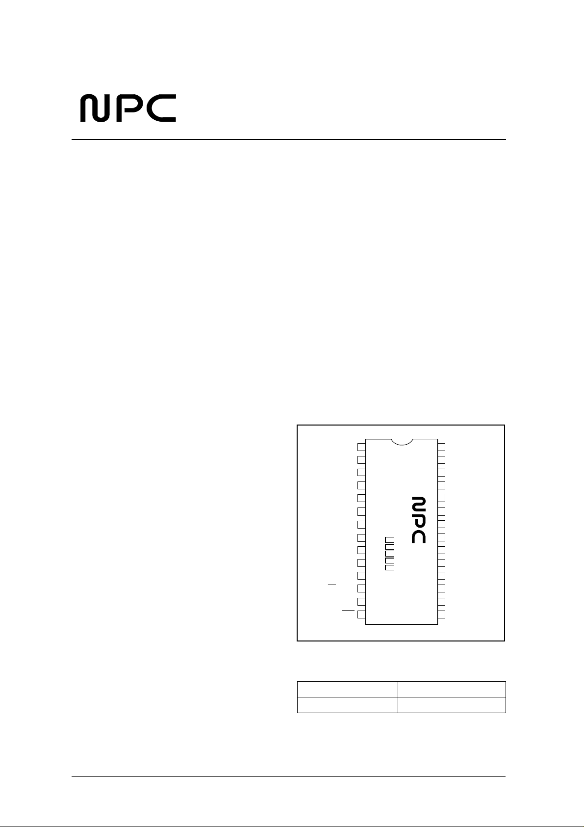
PINOUT
ASEL2/MDCK
SYNC/MDLE
ORDERING INFOMATION
(TOP VIEW)
1
DIN
2
BCKI
3
VDD1
4
DITH
CKEN
5
6
XTI
7
XTO
8
VSS1
CKO
9
CKS
10
11
HS/MDT
SM5846AP 28pin DIP
12
13
RST
14
Device Package
SM5846AP
28
27
26
25
24
23
22
21
20
19
18
17
16
15
LRCI
MDS
BCKO
WCKO
DOL
DOR
VDD2
VSS2
ASEL1
OBS
TEST2
TEST1
DEEM
LRS
Audio
ICs
NIPPON PRECISION CIRCUITS—1
Page 2
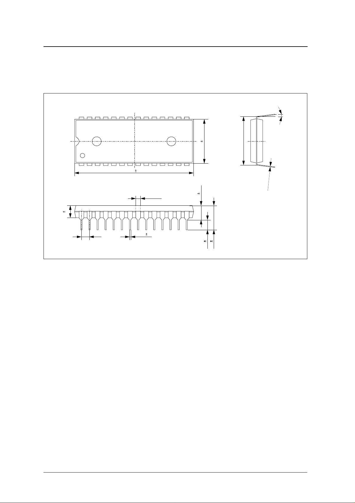
PACKAGE DIMENSIONS
Unit: mm
SM5846AP
28-pin plastic DIP
3.8 0.1
2.54
37.3 0.3
0.45 0.1
1.5
+
−
0.3
0.05
13.8 0.2
4.5 0.3
3.2 0.2
3.2 0.2
7.7 0.5
15.2
+
0.10
0.25
0.05
−
Audio
ICs
0° to 15°
NIPPON PRECISION CIRCUITS—2
Page 3
≥
SM5846AP
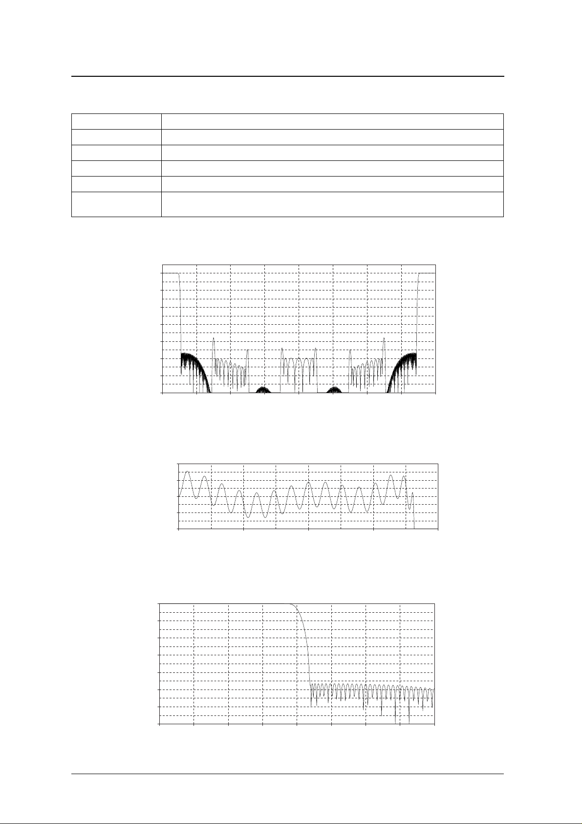
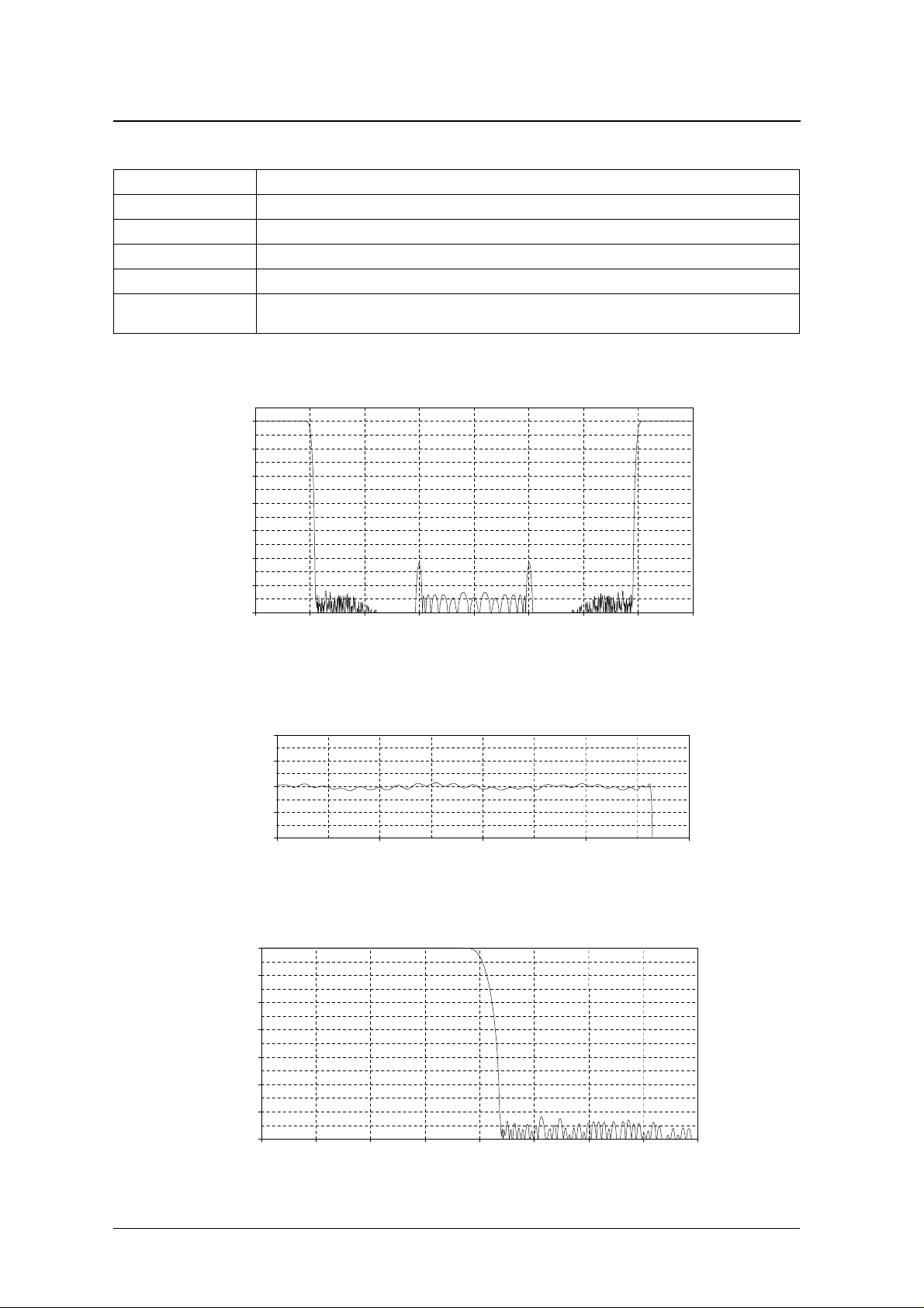
FILTER CHARACTERISTICS
Normal-speed Sampling
Parameter Rating
Passband bandwidth 0 to 0.4535fs
Stopband bandwidth 0.5465 to 7.4535fs
Passband ripple ±0.0004 dB
Stopband attenuation
Group delay time
1
When CKS is HIGH: 63.89/fs (when SYNC is LOW) and 63.51/fs to 64.26/fs (when SYNC is HIGH)
When CKS is LOW: 63.76/fs (when SYNC is LOW) and 63.59/fs to 64.14/fs (when SYNC is HIGH)
1. The time difference due to digital filter operation between the end of serial data input (at rate fs) and the start of serial data output (at rate 8fs).
Overall frequency characteristic
0
75 dB
Audio
ICs
20
40
(dB)
60
80
100
Attenuation
120
140
0.0 1.0 2.0 3.0 4.0 5.0 6.0 7.0 8.0
Passband frequency characteristic
-0.0005
-0.00025
0.00000
0.00025
Attenuation (dB)
0.0005
0.000 0.125 0.250 0.375 0.500
Frequency
Frequency
(fs)
(fs)
Transition band characteristic
0
20
40
(dB)
60
80
100
Attenuation
120
140
0.00 0.125 0.25 0.375 0.50 0.625 0.75 0.825 1.00
Frequency
(fs)
NIPPON PRECISION CIRCUITS—3
Page 4
≥
SM5846AP
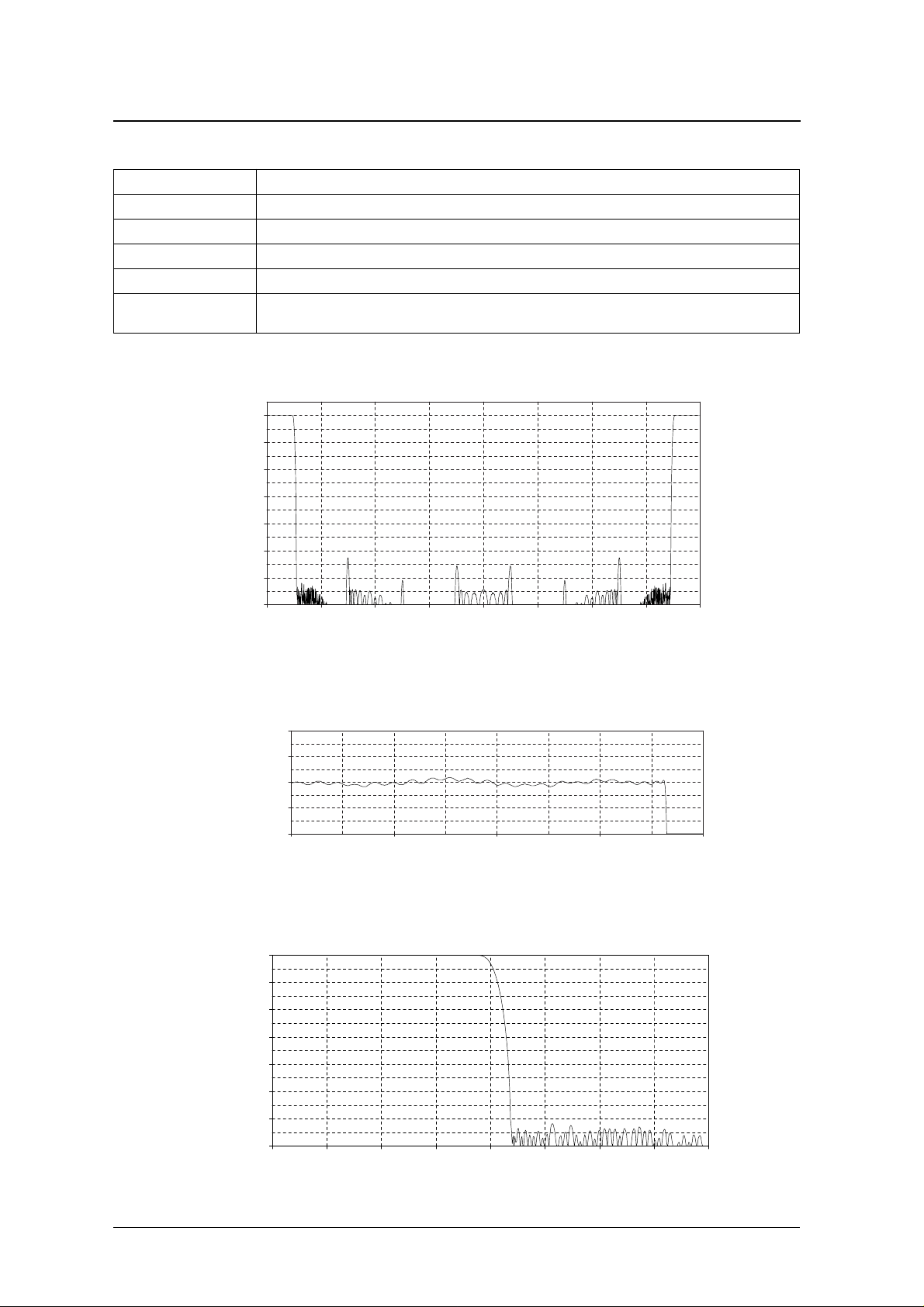
High-speed Sampling (8fs Output)
Parameter Rating
Passband bandwidth 0 to 0.4535fs
Stopband bandwidth 0.5465 to 7.4535fs
Passband ripple ±0.00001 dB
Stopband attenuation
Group delay time
1
When CKS is HIGH: 51.91/fs (when SYNC is LOW) and 51.53/fs to 52.28/fs (when SYNC is HIGH)
When CKS is LOW: 51.78/fs (when SYNC is LOW) and 51.40/fs to 52.15/fs (when SYNC is HIGH)
1. The time difference due to digital filter operation between the end of serial data input (at rate fs) and the start of serial data output (at rate 8fs).
Overall frequency characteristic
0
20
105 dB
Audio
ICs
40
(dB)
60
80
100
Attenuation
120
140
0.0 1.0 2.0 3.0 4.0 5.0 6.0 7.0 8.0
Passband frequency characteristic
-0.0001
-0.00005
(dB)
0.00000
0.00005
Attenuation
0.0001
0.000 0.125 0.250 0.375 0.500
Transition band characteristic
Frequency
Frequency
(fs)
(fs)
0
20
40
(dB)
60
80
100
Attenuation
120
140
0.00 0.125 0.25 0.375 0.50 0.625 0.75 0.825 1.00
Frequency
(fs)
NIPPON PRECISION CIRCUITS—4
Page 5
≥
SM5846AP
High-speed Sampling (4fs Output)
Parameter Rating
Passband bandwidth 0 to 0.4535fs
Stopband bandwidth 0.5465 to 7.4535fs
Passband ripple ±0.00001 dB
Stopband attenuation
Group delay time
1
When CKS is HIGH: 50.78/fs (when SYNC is LOW) and 50.40/fs to 51.15/fs (when SYNC is HIGH)
When CKS is LOW: 50.77/fs (when SYNC is LOW) and 50.40/fs to 51.15/fs (when SYNC is HIGH)
1. The time difference due to digital filter operation between the end of serial data input (at rate fs) and the start of serial data output (at rate 8fs).
Overall frequency characteristic
0
104 dB
Audio
ICs
20
40
(dB)
60
80
Attenuation
100
120
140
0.0 0.5 1.0 1.5 2.0 2.5 3.0 3.5 4.0
Passband frequency characteristic
-0.0001
-0.00005
(dB)
0.00000
0.00005
Attenuation
0.0001
0.000 0.125 0.250 0.375 0.500
Frequency
Frequency
(fs)
(fs)
Transition band characteristic
0
20
40
(dB)
60
80
100
Attenuation
120
140
0.125 0.25 0.375 0.50 0.625 0.75 0.825 1.00
Frequency
(fs)
NIPPON PRECISION CIRCUITS—5
Page 6
SM5846AP
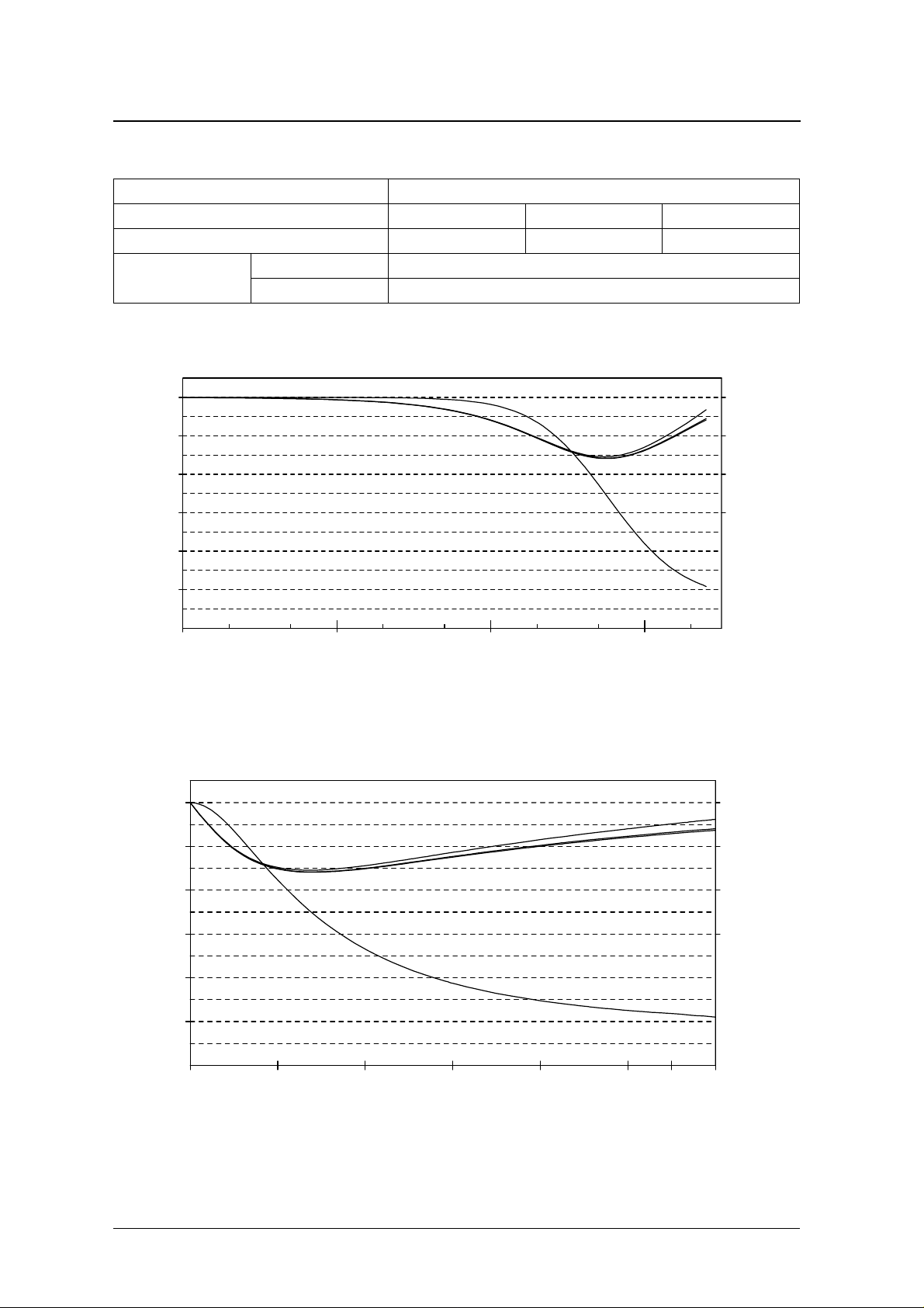
Deemphasis Filter Characteristics (Normal-speed Sampling)
Parameter Rating
Sampling frequency (fs) 32 kHz 44.1 kHz 48 kHz
Passband bandwidth 0 to 14.5 kHz 0 to 20.0 kHz 0 to 21.7 kHz
Deviation from ideal
characteristics
Deemphasis passband characteristic (logarithmic scale)
The phase traces are from top to bottom fs = 32/44.1/48 kHz, respectively.
Attenuation ±0.01 dB
Phase 0 to 6
°
Audio
ICs
0
2
4
6
8
Attenuation (dB)
10
10 20 50 100 200 500 1k 2k 5k 10k 20k
Frequency (Hz)
Deemphasis passband characteristic (linear scale)
The phase traces are from top to bottom fs = 32/44.1/48 kHz, respectively.
0
2
Phase
Attenuation
Phase
0
-20
-40
Phase θ ( ° )
-60
0
-20
4
6
Attenuation (dB)
8
Attenuation
10
0 4k 8k 12k 16k 20k 22k 24k
Frequency (Hz)
NIPPON PRECISION CIRCUITS—6
-40
Phase θ ( ° )
-60
Page 7
SM5846AP
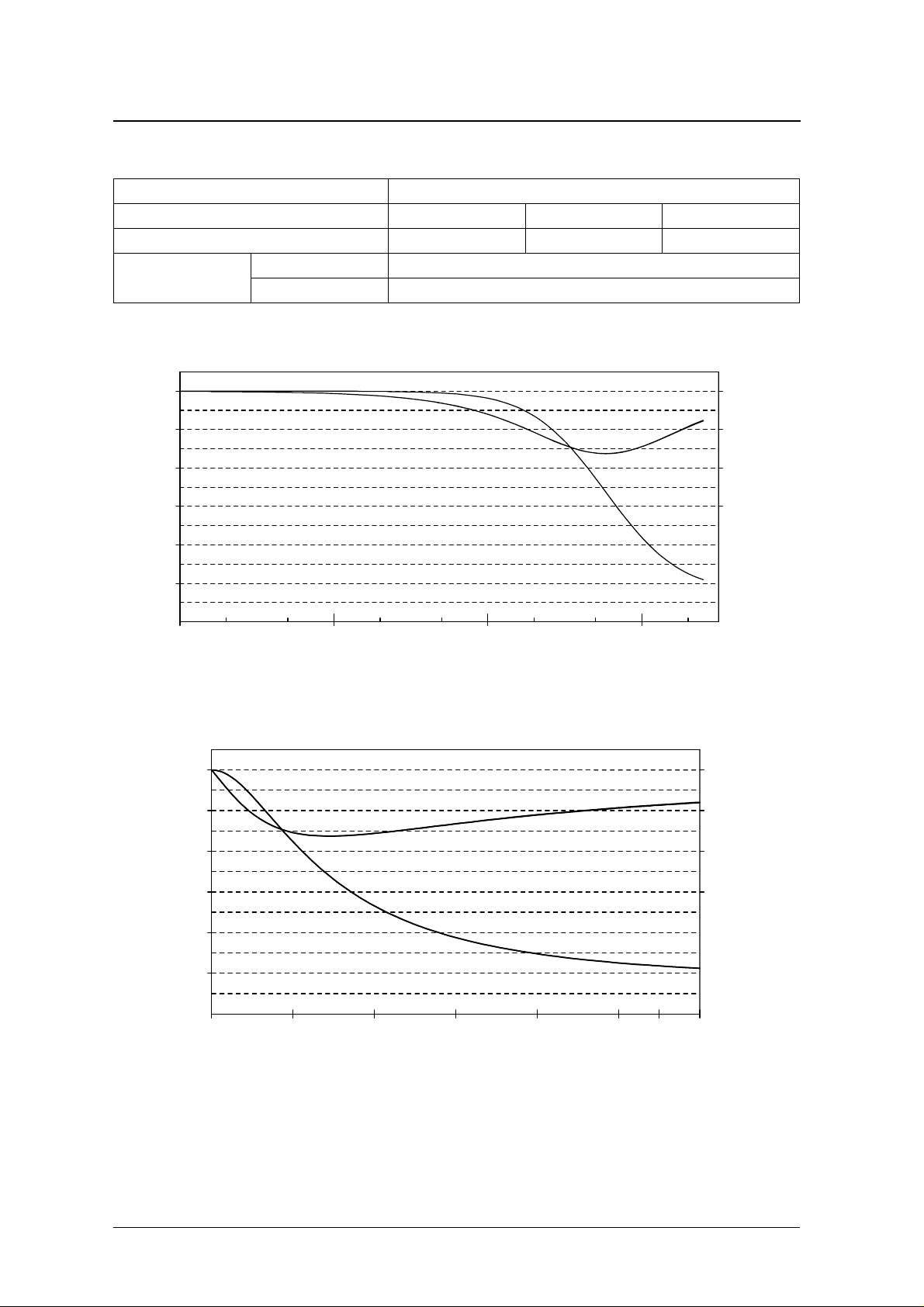
Deemphasis Filter Characteristics (High-speed Sampling)
Parameter Rating
Sampling frequency (fs) 64 kHz 88.2 kHz 96 kHz
Passband bandwidth 0 to 29.0 kHz 0 to 40.0 kHz 0 to 43.5 kHz
Deviation from ideal
characteristics
Deemphasis passband characteristic (logarithmic scale)
The phase traces are from top to bottom fs = 64/88.2/96 kHz, respectively.
Attenuation ±0.001 dB
Phase 0 to 1
°
Audio
ICs
0
2
4
6
Attenuation (dB)
8
10
10 20 50 100 200 500 1k 2k 5k 10k 20k
Frequency (Hz)
Deemphasis passband characteristic (linear scale)
The phase traces are from top to bottom fs = 64/88.2/96 kHz, respectively.
0
2
Phase
Attenuation
Phase
0
-20
-40
Phase θ ( ° )
-60
0
-20
4
6
8
Attenuation (dB)
10
0 4k 8k 12k 16k 20k 22k 24k
Frequency (Hz)
Attenuation
NIPPON PRECISION CIRCUITS—7
-40
-60
Phase θ ( ° )
Page 8
SM5846AP
SPECIFICATIONS
Absolute Maximum Ratings
V
= 0 V
SS
Parameter Symbol Rating Unit
Supply voltage range V
Input voltage range V
Storage temperature range T
Power dissipation P
Soldering temperature T
Soldering time t
Recommended Operating Conditions
−
−
+
−
°
°
−
° C
−
Audio
ICs
DD
IN
stg
D
sld
sld
0.3 to 7.0 V
0.3 to V
0.3 V
DD
40 to 125
750 mW
255
10 s
C
C
V
= 0 V
SS
Parameter Symbol Rating Unit
Supply voltage range V
Operating temperature range T
DC Electrical Characteristics
V
= 4.5 to 5.5 V, V
DD
Parameter Symbol Condition
Supply current consumption
HIGH-level input voltage V
LOW-level input voltage V
XTI AC-coupled input voltage V
HIGH-level output voltage V
LOW-level output voltage V
XTI HIGH-level input current I
XTI LOW-level input current I
LOW-level input current I
Input leakage current I
1. V
= 5.0 V , f
DD
= 18.432 MHz, 384fs operation, no output load.
sys
= 0 V, T
SS
1
= − 20 to 70 ° C
a
I
DD
IH
IL
INAC
OH
OL
IH
IL
IL
LH
All inputs 0.7V
All inputs – – 0.3V
All outputs, I
All outputs, I
V
= V
IN
DD
V
= V
IN
SS
Inputs excluding XTI,
V
= V
IN
SS
Inputs excluding XTI,
V
= DV
IN
DD
opr
4.5 to 5.5 V
20 to 70
Rating
min typ max
– 110 130 mA
DD
0.3V
DD
= − 1 mA V
OH
= 2 mA – – 0.4 V
OL
0.4 – – V
DD
––V
DD
––V
–1020µA
–1020µA
–1020µA
DD
– – 1.0 µA
Unit
V
p-p
NIPPON PRECISION CIRCUITS—8
Page 9
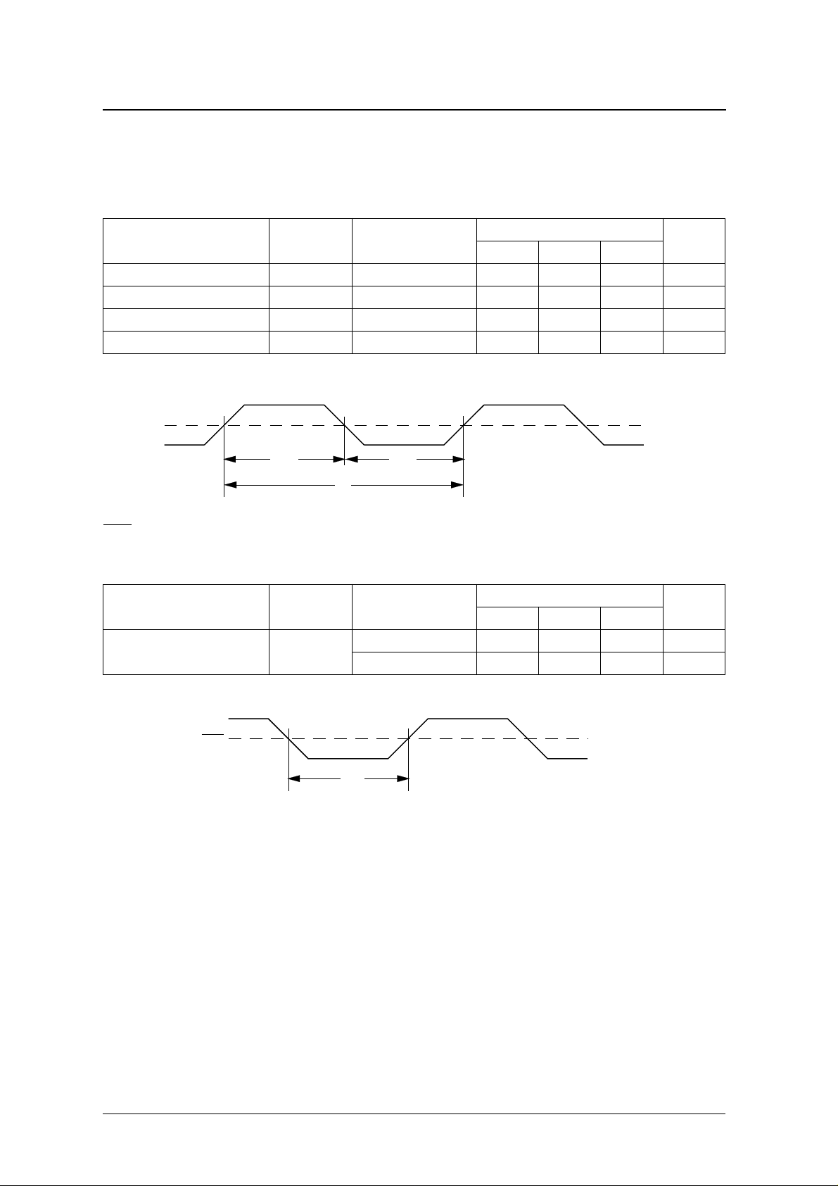
AC Characteristics
XTI input timing
SM5846AP
VDD = 4.5 to 5.5 V, VSS = 0 V, Ta = −20 to 70 °C
Parameter Symbol Condition
Oscillator frequency f
XTI clock pulse cycle time t
XTI HIGH-level clock pulsewidth t
XTI LOW-level clock pulsewidth t
OSC
XI
CWH
CWL
XTI
tCHW tCHW
tXI
RST input timing
VDD = 4.5 to 5.5 V, VSS = 0 V, Ta = −20 to 70 °C
Parameter Symbol Condition
Reset pulsewidth t
RST
When power is applied 1 – – µs
At all other times 50 – – ns
Audio
ICs
Rating
Unit
min typ max
10 – 18.5 MHz
54 – – ns
24 – – ns
24 – – ns
0.5VDD
Rating
Unit
min typ max
RST
0.5VDD
tRST
NIPPON PRECISION CIRCUITS—9
Page 10
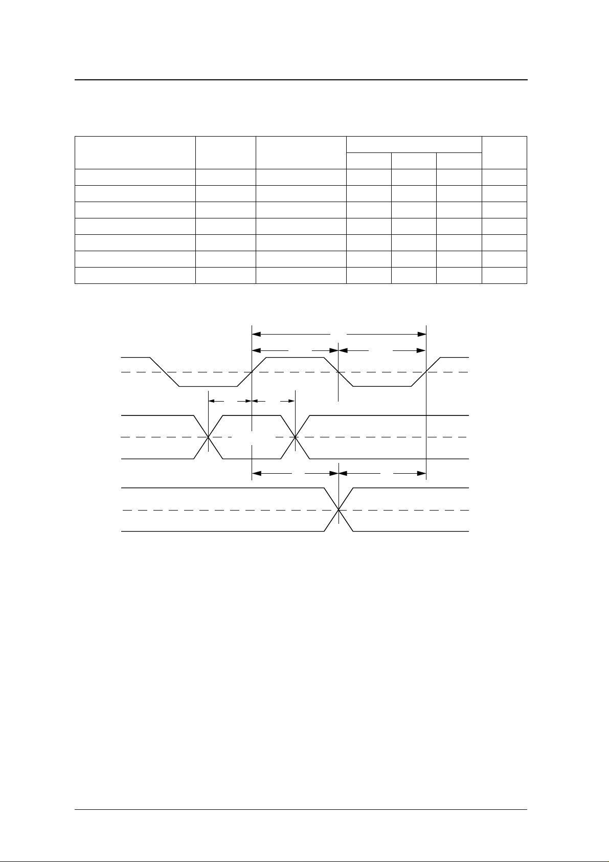
Serial data input timing (BCKI, DIN, LRCI)
VDD = 4.5 to 5.5 V, VSS = 0 V, Ta = −20 to 70 °C
SM5846AP
Parameter Symbol Condition
BCKI pulse cycle time t
BCKI HIGH-level pulsewidth t
BCKI LOW-level pulse width t
DIN setup time t
DIN hold time t
BCKI rising edge to LRCI edge time t
LRCI edge to BCKI rising edge time t
BCKI
DIN
BCY
BCWH
BCWL
DS
DH
BL
LB
tDS
VALID
VALID
VALID
tBCY
tBCWH tBCWL
tDH
Rating
Unit
min typ max
100 – – ns
50 – – ns
50 – – ns
20 – – ns
20 – – ns
50 – – ns
50 – – ns
0.5VDD
0.5VDD
Audio
ICs
LRCI
tBL
tLB
0.5VDD
NIPPON PRECISION CIRCUITS—10
Page 11
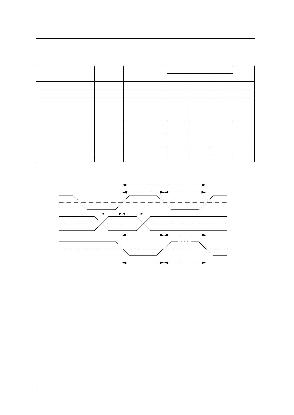
SM5846AP
Microprocessor serial interface timing (MDCK, MDT, MDLE)
VDD = 4.5 to 5.5 V, VSS = 0 V, Ta = −20 to 70 °C
Parameter Symbol Condition
MDCK pulse cycle time t
MDCK HIGH-level pulsewidth t
MDCK LOW-level pulsewidth t
MDT setup time t
MDT hold time t
MDCK rising edge to MDLE edge
time
MDLE edge to MDCK rising edge
time
MDLE HIGH-level pulsewidth t
MDLE LOW-level pulsewidth t
MDCK
MCY
MCWH
MCWL
MDS
MDH
t
MCL
t
MLC
MLWH
MLWL
tMCWH
tMCY
Rating
Unit
min typ max
100 – – ns
50 – – ns
50 – – ns
20 – – ns
20 – – ns
50 – – ns
50 – – ns
20 – – ns
20 – – ns
tMCWL
0.5VDD
Audio
ICs
MDLE
tMDS tMDH
tMCL
tMCL
tMLWL tMLWH
0.5VDDMDT
0.5VDD
NIPPON PRECISION CIRCUITS—11
Page 12

SM5846AP
Output signal timing (CKO, BCKO, DOR, DOL, WCKO)
VDD = 4.5 to 5.5 V, VSS = 0 V, Ta = −20 to 70 °C, CL = 15 pF
Parameter Symbol Condition
XTI to CKO propagation delay time
XTI to BCKO propagation delay time
BCKO to DOR propagation delay
time
BCKO to DOL propagation delay time
BCKO to WCKO propagation delay
time
CKO output
XTI
t
CKH
t
CKL
t
t
t
t
t
bdH
t
t
bdH
t
t
bdH
t
sbH
sbL
sbH
sbL
bdL
bdL
bdL
Normal and high-speed
mode 4fs output
High-speed mode 8fs
output
Rating
min typ max
–1735
–1735
–2060
–2060
–2060
–2060
−5–15
−5–15
−5–15
−5–15
−5–15
−5–15
0.5VDD
Unit
ns
ns
ns
ns
ns
Audio
ICs
CKO
tCKH
tCKL
1.5V
NIPPON PRECISION CIRCUITS—12
Page 13

BCKO output
XTI
SM5846AP
tsbH
0.5VDD
Audio
ICs
BCKO *1
BCKO *2
DOR, DOL, WCKO output
BCKO
DOR
DOL
WCKO
tsbL
tsbL
tsbH
*1 : High speed mode 8fs output
*2 : Normal and high-speed mode 8fs output
tbdH tbdL
1.5V
1.5V
1.5V
1.5V
NIPPON PRECISION CIRCUITS—13
Page 14

PIN DESCRIPTION
SM5846AP
Number Name I/O
1 DIN Ip Data input
2 BCKI Ip Bit clock input
3 VDD1 – 5 V supply voltage
4 DITH Ip Dither ON/OFF control
5 CKEN Ip Crystal oscillator operation enable
6 XTI I Crystal oscillator input/external clock input
7 XTO O Crystal oscillator output
8 VSS1 – Ground
9 CKO O Master clock output
10 CKS Ip Master clock input frequency select
11 ASEL2/MDCK Ip Operating mode select/microprocessor interface clock input
12 HS
13 SYNC/MDLE Ip Sync mode select/microprocessor interface latch enable input
14 RST Ip Reset input
15 LRS Ip LR clock polarity select
16 DEEM Ip Deemphasis ON/OFF select
17 TEST1 Ip Test pin 1. Tie HIGH or leave open for normal operation.
18 TEST2 Ip Test pin 2. Tie LOW for normal operation.
19 OBS Ip Output data length select
20 ASEL1 Ip Operating mode select
21 VSS2 – Ground
22 VDD2 – 5 V supply voltage
23 DOR O Right-channel data output
24 DOL O Left-channel data output
25 WCKO O Word clock output
26 BCKO O Output data bit clock output
27 MDS Ip Mode set method select
28 LRCI Ip LR cloc k input
/MDT Ip Operating mode select/microprocessor interface data input
1
Description
Audio
ICs
1. Ip = input pin with pull-up resistor, I = input, O = output
NIPPON PRECISION CIRCUITS—14
Page 15

BLOCK DIAGRAM
XTI
XTO
CKO
CKEN
CKS
SM5846AP
RST
VDD2
VDD1
VSS2
VSS1
Audio
ICs
DIN
BCKI
LRCI
LRS
Clock Generator
Output data
Interface
(serial input)
Control
Micro controller
Interface
(serial input)
Reset Circuit
Arithmetic Block
Control
DEEM
TEST2
TEST1
SYNC/MDLE
Output data
Interface
(serial output)
Control
Operation Mode
Control
MDS
HS/MDT
ASEL2/MDCK
DOR
DOL
BCKO
WCKO
OBS
DITH
ASEL1
NIPPON PRECISION CIRCUITS—15
Page 16

SYSTEM CONFIGURATION
DIN
BCKI
LRCI
DSP
CKO
MDS
CKEN
SM5846AP
Setting
ASEL1
HS/MDT
ASEL2/MCK
XTI
XTO
LRS
DITH
DEEN
SYNC/MLE
CKS
VSS1
OBS
VSS2
TEST2
VDD1
VDD2
+5V
TEST1
RST
DOR
DOL
BCKO
WCKO
DAC
Oscilation
Control
DATA FLOW
ATT1/ATT2 soft muting uses the D-ATT function to set the gain to −∞.
Normal-speed sampling (fs = 32/44.1/48 kHz)
FIRI
(fs)
IN
(×2)
LPF
fs
2fs 2fs 2fs 2fs 4fs
SWa (121 order)
High-speed sampling (fs = 64/88.2/96 kHz)
FIR4
LPF
fs 2fs
IN
(fs)
(×2)
2fs
SWb(177 order)
DEMI DLY ATT1 FIR2 FIR3
2fs
4fs
2fs 2fs 2fs
FIR5
LPF
4fs
(×2)
(29 order)
4fs
SWd(ON / OFF)
Setting
DEM2
+5V+5V
(D-ATT / Soft Mute)
ATT2
4fs
4fs
(D-ATT / Soft Mute)
LPF
4fs
(×2)
(21 order) (13 order)
FIR6
LPF
4fs
8fs
(17 order)
(×2)
8fs
4fs
8fs
Reset Circuits
LPF
(×2)
SWg ( 8fs / 4fs )
8fs
8fs/4fs
OUT
(8fs)
OUT
( 8fs / 4fs )
NIPPON PRECISION CIRCUITS—16
Page 17

SM5846AP
FUNCTIONAL DESCRIPTION
Mode Switching and Function Switching
The SM5846AP supports several operating modes and
function switches. Internal control flags, set by the digital
inputs or serial data input signal from a microprocessor,
determine the status of those function switches.
Mode switching/function switch controls
Stage Name
System M DS Yes IC control request switch (input pin/control flag)
HS Yes Yes
Operating mode switch
ASEL1 Yes Yes
Clock switch
Filter switch
Input interface switch
Output interface switch OBS Y es Yes Output data length set
CKS Yes Input clock frequency switching
CKEN Yes Crystal oscillator operating control switching
DEEM Yes Yes Deemphasis ON/OFF switching
FSEL2 Yes
FSEL1 Yes
MUTE Yes Mute ON/OFF control
DITH
SYNC Yes Yes Jitter-free/sync mode switching
LRS Yes LRCI (LR clock) input polarity s witching
IBS2 Yes
IBS1 Yes
Control request
Input Control flag
Yes
(pos. logic)
Yes
(neg. logic)
Function
Operating mode switchingASEL2 Yes Yes
Deemphasis filter sampling frequency set
Dither ON/OFF control
Input data length set
Control request switching
MDS input and device control
Mode switching/function switching is performed under
input pin control when MDS is HIGH, and under internal
flag control when MDS is LOW.
1
MDS
HIGH Input pins
LOW Control flags
1. Switching MDS during device operation is prohibited.
Control request
Input pin functions when MDS is LOW
All pins that are part of the microprocessor interface
can be used whenever MDS is LOW.
Pin name Function Notes
HS
/MDT
ASEL2/MDCKSerial data transfer clock
SYNC/MDLE
CK S CKS function switch input
CKEN CKEN function switch input
LRS LRS function switch input
Serial data transfer data
clock
Used for the
input
Serial data transfer latch
enable input
NIPPON PRECISION CIRCUITS—17
microprocessor
interface
Input pin control only
because there is no
corresponding
control flag.
Page 18

SM5846AP
Control flag functions when MSD is HIGH
(default)
Other requests are controlled by internal flag only
because there is no corresponding input pin. These
control flags are valid when MDS is HIGH. The
default values are shown in the following table.
Flag name Default value Default setting
FSEL2 HIGH
FSEL1 HIGH
MUTE
IBS2 LOW
IBS1 HIGH
HIGH Muting OFF
44.1 kHz deemphasis filter
sampling frequency
16-bit input data length
Clock Functions
Input clock frequency switching (CKS)
This switch is used to select the input clock frequency—384fs or 512fs (normal-speed sampling),
and 192fs or 256fs (high-speed sampling).
CKS Input sampling frequency fs (kHz)
Frequency (MHz) (× fs)
32 16.384 512fs Normal-speed sampling mode
LOW
64 16.384 256fs High-speed sampling mode
32 12.288
48 18.432
HIGH
64 12.288
96 18.432
Crystal oscillator control switch (CKEN)
This switch is used to start/stop the crystal oscillator
circuit.
CKEN Crystal oscillator operation
HIGH Oscillating
LOW Stopped
System clock
Notes
384fs Normal-speed sampling mode44.1 16.9344
192fs High-speed sampling mode88.2 16.9344
NIPPON PRECISION CIRCUITS—18
Page 19

Crystal oscillator circuit
SM5846AP
The built-in crystal oscillator circuit comprises a
feedback resistor and several logic gates. The system
Rf
XTICKEN
X'tal
Oscilation/Stop
Contorol
C1
clock can be generated using an external quartz crystal and 2 capacitors.
System
Clock
XTO
C2
CKO
System Clock
Output
External clock
When an external clock is used, XTO is left opencircuit and the clock signal is input on XTI.
Rf
XTICKEN
Oscilation/ Stop
Contorol
External Clock
Input
Open
XTO
System
Clock
CKO
System Clock
Output
NIPPON PRECISION CIRCUITS—19
Page 20

SM5846AP
Other control settings
Input data length select
ISB1 and ISB2 flags are used to set the input data
length.
IBS2 IBS1
HIGH HIGH 20 bits
HIGH LOW 24 bits
LOW HIGH 16 bits
LOW LOW 32 bits
LRCI input polarity select
Input data
length
Notes
The length is set to the
default value of 16 bits
(IBS2 = LOW and IBS1 =
HIGH) after a reset.
Pin LRS is used to set the LRCI input polarity.
LRS LRCI Input channel
HIGH HIGH Left
HIGH LOW Right
LOW HIGH Right
LOW LOW Left
Sync mode select
Filter Stage
Operating mode
The SM5846A supports 3 different operating modes
to control output data rate switching. The operating
mode is selected by the state of HS, ASEL1 and
ASEL2.
HS ASEL1 ASEL2
HIGH LOW HIGH
LOW HIGH
1. Only the above 3 modes are valid.
HIGH
LOW 4-times
Operating mode
Speed Oversampling
Normal-speed
sampling
High-speed
sampling
Operating speed and sampling frequency
The SM5846AP supports sampling frequencies of
32/44.1/48 kHz (normal-speed sampling mode) and
64/88.2/96 kHz (high-speed sampling mode).
Operating speed Input sampling frequency
Normal-speed sampling 32/44.1/48 kHz
High-speed sampling 64/88.2/96 kHz
1
8-times
8-times
The SYNC pin or flag setting can be used to select
either jitter-free mode or sync mode to control synchronization between input data and internal arithmetic blocks.
SYNC Mode Notes
HIGH Jitter-free mode
LOW Sync mode
The SYNC flag is set HIGH
(default) after a reset.
Deemphasis filter
The SM5846AP contains a digital deemphasis filter
controlled by DEEM.
DEEM Deemphasis
HIGH ON
LOW OFF
The sampling frequency is selected by FSEL1 and
FSEL2.
Sampling frequency fs (kHz)
FSEL2 FSEL1
HIGH HIGH 44.1 88.2
HIGH LOW 48 96
LOW HIGH 44.1 88.2
LOW LOW 32 64
Normal-speed
sampling
High-speed
sampling
Digital attenuator
The digital attenuator is controlled by serial data
from the microprocessor interface. This data can set
attenuation and muting. Note that the digital attenuator is only enabled when MDS is LOW. ATT1 and
ATT2 are used to set the attenuation in normal-speed
sampling and high-speed sampling, respectively.
NIPPON PRECISION CIRCUITS—20
Page 21

SM5846AP
Attenuation setting
The data stored in the D-ATT attenuation register,
accessed through the microprocessor interface,
determines the attenuation setting of the digital
attenuator. The D-ATT register data format is shown
below.
bit1 bit2 bit3 bit4 bit5 bit6 bit7 bit8
"0" a1 a2 a3 a4 a5 a6 a7
MSB
DATT attenation data (7bit)
Register information
LSB
The attenuation setting is given by the following
equations.
Attenuation 0 [dB]=
Attenuation 20log
Attenuation
127 DATT
–
------------------------------ -
10
128
[dB]=
∞
–=
DATT = 0
()
0 < DATT <127
()
DATT = 127
()
− ∞
The attenuation for a selection of values is given in
the following table.
DATT register
value
0 00H 0 × 1.0
1 01H −0.137 × 0.984375
2 02H −0.206 × 0.9765625
↓↓↓↓
63 3FH −6.021 × 0.5
64 40H −6.157 × 0.4921875
↓↓↓↓
125 7DH −36.12 × 0.015625
126 7EH −42.14 × 0.0078125
127 7F H −
Microprocess
or command
(hex)
Attenuation
(dB)
∞
Relative gain
× 0
Digital attenuator operation
The attenuation register is reset to 0 (attenuation = 0
dB) after a system reset signal.
When data is written to the attenuation register,
through the microprocessor interface, the attenuation
changes from the current value to the new value at
the speed shown in the following table.
Operating speed
Normal-speed
sampling
High-speed sampling 16/fs per step change
Speed of
attenuation change
8/fs per step change
Soft muting operation
Time from min. to
max. attenuation
1016/fs (23.0 ms at
44.1 kHz)
2032/fs (23.0 ms at
88.2 kHz)
Soft muting ON/OFF is controlled by the MUTE
flag, accessed through the microprocessor interface.
Muting Notes
MUTE
HIGH OFF
LOW ON
The MUTE
system reset.
flag is set HIGH (default) after a
When muting is ON, the attenuation ramps down to
at the speed shown in the table. Similarly when
muting is OFF, the attenuation level returns to the
original value at the same speed.
If the contents of the DATT attenuation register are
changed while muting is ON (attenuation = − ∞ ),
only the register contents are replaced. If muting is
subsequently turned OFF, the attenuation value
changes to the new value at the same speed as shown
in the table.
NIPPON PRECISION CIRCUITS—21
Page 22

Output data round-off
,
,
SM5846AP
Output data round-off processing is required because
the internal data length of the digital filter is different
from the output data length (internal data processing
width > output data width).
The SM5846AP can select either normal round-off
or dither round-off on the output data. Round-off
processing can be selected either by input pin or control flag settings.
MDS
HIGH
LOW
DITH
pin
HIGH
LOW
Normal round-off
DITH
flag
HIGH
LOW
Output
data
round-off
Dither
round-off
Normal
round-off
Normal
round-off
Dither
round-off
Notes
The DITH
flag is set
HIGH (default) after a
system reset.
Normal round-off is carried out by adding 1/2 LSB
to the filter output data to form 20/24-bit output data,
depending on the selected output data length.
Dither round-off
Dither round-off is carried out by adding a pseudorandom number between 0 and 1 LSB, derived from
a rectangular distribution, to the filter output data to
form 20/24-bit output data, depending on the
selected output data length. The random number
rectangular distribution is shown below (average =
1/2 LSB).
Probavility
,,,,,,
,,,,,,
0 1/2 1 (LSB)
×
×
Overflow limiter
If an overflow or underflow condition occurs after
round-off or filter arithmetic processing, the output
data will be fixed at positive or negative maximum
value.
NIPPON PRECISION CIRCUITS—22
Page 23

SM5846AP
Audio Data Input Interface
Serial data transmission is used for the digital audio
data input.
The data has the following format:
■
16/20/24/32-bit data length
■
Alternating left/right-channel serial data transmission
■
MSB first
■
Rear packed
■
2s complement for negative values
Audio data input interface schematic
Audio data input interface pins
Audio data is input using pins LRCI, BCKI, and
DIN. The LRCI input polarity is determined by pin
LRS.
Pin name Function
LRCI Left/right-channel latch clock input
BCKI Bit transfer clock input
DIN Serial data input
LRS LRCI input polarity switch
Serial data on DIN is input to the serial-to-parallel
shift register on the falling edge of the bit transfer
clock BCKI. The parallel data is then stored in the
left/right-channel input buffers on the HIGH/LOWlevel pulse of the LRCI latch clock signal, depending on the selected polarity of the LRCI clock.
Audio
ICs
DIN
BCKI
LRCI
LRS
D
Left channel
C
Input Data Buffer
Q
Left channel
Input Data
32bit SIPO Shiftregister
D
C
32bit Register
Q
D
Right channel
C
Input Data Buffer
Q
Right channel
Input Data
32bit Register
NIPPON PRECISION CIRCUITS—23
Page 24

Input data interface example (LRS = HIGH)
32-bit input data length
SM5846AP
(MSB)
DIN
BCKI
(64fs)
LRCI
24-bit input data length
DIN
BCKI
(64fs)
LRCI
fs
Left channel Input Data
(LSB)
31
30
29 28 2 1 0 31 30 29 28 2 01
Right channel Input Data
(MSB)
fs
Left channel Input Data
(MSB) (LSB)
23 22 2 1 0 23 22 2 01
Right channel Input Data
(MSB)
(LSB)
(LSB)
Audio
ICs
20-bit input data length
DIN
BCKI
(64fs)
LRCI
16-bit input data length
DIN
BCKI
(64fs)
fs
Left channel
Input Data
(MSB)
19 18 2 1 0 19 18 2 01
Left channel
Input Data
(MSB) (LSB) (MSB) (LSB)
15 14 1 0 15 14 1 0
(LSB) (MSB) (LSB)
fs
Right channel
Input Data
Right channel
Input Data
LRCI
NIPPON PRECISION CIRCUITS—24
Page 25

Input data validity
,
32-bit input data length
SM5846AP
31 30 28 26 24
Polarity
Mark
24-bit input data length
Decimal point
23 22 20 18 16 6 4 2 0
Polarity
Mark
20-bit input data length
Effective Number of Bits (24bits)
Decimal point
8 6 4 2 0
,,,,,,,,,,,,,,,,,
Input Data (32bits)
Effective Number of Bits (24Bits)
Input Data (24Bits)
Low order 8 bits cut it off
(No round-offattention)
19 18 16 14 4 2 0
Polarity
Mark
16-bit input data length
15 14 12 2 0
Polarity
Mark
Decimal point
Decimal point
Input Data (16bits)
Effective Number of bits (24bits)
Input Data (20bits)
00 0 0 0 0 0 0 0
Effective Number of Bits (24bits)
0 0 0 0
Input to "0"(4 bits)
Input to "0"(8 bits)
NIPPON PRECISION CIRCUITS—25
Page 26

SM5846AP
Audio Data Output Interface
Serial data transmission is used for the digital audio
data output.
The data has the following format:
■
20/24-bit data length
■
Simultaneous left/right-channel serial data transmission
■
MSB first
■
Bit transfer clock burst (NPC format)
■
2s complement for negative values
Audio data output interface pins
Audio data is output using pins WCKO, BCKO, DOL
and DIN.
Pin name Function
WCKO Word clock output
BCKO Bit transfer clock output
DOL Left-channel serial data output
DOR Right-channel serial data output
Serial data is output on DOL and DOR on the falling edge of the bit transfer clock BCKO. Generally,
external circuits, such as a serial D/A converter,
sample the serial data output on DOL and DOR on
the rising edge of the bit transfer clock signal, and
then shift the data into a register. At the completion
of one data cycle (20/24-bit selectable) transfer, the
word clock WCKO goes LOW with a 50% duty
ratio. Then the external circuit writes parallel data to
a buffer register on the falling edge of word clock
WCKO.
Output data length select
The output data length is set by either the OBS pin
or flag.
OBS
HIGH 24 bits
LOW 20 bits
Output data
length
Notes
The OBS flag is set LOW
(default) after a system reset.
Audio
ICs
NIPPON PRECISION CIRCUITS—26
Page 27

Audio data output interface
DOL
L-ch Serial DAC
D
C
STB
R-ch Serial DAC
SM5846AP
Following Block
VO
VOUT(L-ch)
Audio
ICs
DOR
BCKO
WCKO
output data format
24-bit output data length
23 22 20 18 16 6 4 2 0
D
C
STB
D
C
D
20/24bit
SIPO
Shiftregister
20/24bit SIPO
Shiftregister
IN
DAC
VO
VOUT(R-ch)
Polarity
Mark
Decimal point
20-bit output data length
19 18 16 14 4 2 0
Polarity
Mark
Output Data (24bits)
Decimal point
Output Data (20bits)
NIPPON PRECISION CIRCUITS—27
Page 28

SM5846AP
Audio data output timing
Normal-speed sampling: 384fs clock, 24-bit data output, 8fs output data rate
1 frame (1/8fs)
CK/2
f
(192fs)
WCKO
BCKO
DOL
11012 2420
Audio
ICs
212223 20
DOR
MSB
24bits
Normal-speed sampling: 384fs clock, 20-bit data output, 8fs output data rate
1 frame (1/8fs)
212 24
fCK/2
(192fs)
WCKO
BCKO
DOL
110 2021
2310
LSB
DOR
1819 17 1 0
LSBMSB
20bits
NIPPON PRECISION CIRCUITS—28
Page 29

SM5846AP
Normal-speed sampling: 512fs clock, 24-bit data output, 8fs output data rate
1 frame (1/8fs)
21416 3225
CK/2
f
(256fs)
WCKO
BCKO
DOL
DOR
11315 17 3018
2223 21 0
MSB
LSB
24bits
Normal-speed sampling: 512fs clock, 20-bit data output, 8fs output data rate
Audio
ICs
f
CK/2
(256fs)
WCKO
BCKO
DOL
DOR
1 frame (1/8fs)
21416 3221
11315 17 3018 19 20
1819 17 0
MSB
20bits
LSB
NIPPON PRECISION CIRCUITS—29
Page 30

SM5846AP
High-speed sampling: 192fs clock, 24-bit data output, 8fs output data rate
1 frame (1/8fs)
21012 24
CK
f
(192fs)
WCKO
BCKO
DOL
1
Audio
ICs
20 21
2223 21 0
DOR
MSB
20 321
24bits
High-speed sampling: 192fs clock, 20-bit data output, 8fs output data rate
1 frame (1/8fs)
21012 24
fCK
(192fs)
WCKO
BCKO
DOL
1 20 21
LSB
DOR
18 17 0
MSB
20bits
119
LSB
NIPPON PRECISION CIRCUITS—30
Page 31

SM5846AP
High-speed sampling: 256fs clock, 24-bit data output, 8fs output data rate
1 frame (1/8fs)
21314
f
CK
1
15 16 17 18 25 30 32
(256fs)
WCKO
BCKO
DOL
22 21 0
23
DOR
MSB
24bits
High-speed sampling: 256fs clock, 20-bit data output, 8fs output data rate
Audio
ICs
LSB
CK
f
(256fs)
WCKO
BCKO
DOL
DOR
1 frame (1/8fs)
21314
1
18 17 0
19
15 16 17 18 19 20 21 30 32
MSB
20bits
LSB
NIPPON PRECISION CIRCUITS—31
Page 32

SM5846AP
High-speed sampling: 192fs clock, 24-bit data output, 4fs output data rate
1 frame (1/4fs)
fCK/2
(96fs)
WCKO
BCKO
DOL
DOR
1
22 21 3
23
20 210
MSB
10
12 20 24
LSB
24bits
High-speed sampling: 192fs clock, 20-bit data output, 4fs output data rate
1 frame (1/4fs)
CK/2
f
(96fs)
WCKO
BCKO
DOL
DOR
MSB
1
19 18
17
10
12
21
20
0
1
24
LSB
20bits
NIPPON PRECISION CIRCUITS—32
Page 33

SM5846AP
High-speed sampling: 256fs clock, 24-bit data output, 4fs output data rate
1 frame (1/4fs)
18
17
25
CK/2
f
(128fs)
WCKO
BCKO
DOL
DOR
1
MSB
2
23 22
14
13
21
16
15
24bits
High-speed sampling: 256fs clock, 20-bit data output, 4fs output data rate
0
LSB
30
32
fCK/2
(128fs)
WCKO
BCKO
DOL
DOR
1
2
19 18
MSB
1 frame (1/4fs)
13 15 16 17 18 30
14
17
19 20 21
0
32
LSB
20bits
NIPPON PRECISION CIRCUITS—33
Page 34

SM5846AP
Microprocessor Interface
Microprocessor interface pins
When MDS is LOW, the SM5846AP is controlled by
internal flags set by serial data transferred over the
microprocessor interface comprising MDLE, MDCK
and MDT.
Pin name Function
MDLE Microprocessor data latch enable input
MDCK Microprocessor data transfer clock input
8bit SIPO Shift Register
MDT
MDCK
D
C
Q
8bit Register
D
D
C
C
Q
Q
Pin name Function
MDT Serial data input
Internal control flag serial data on MDT is input into
an internal shift register on the rising edge of
MDCK. After 8-bit data has been input, the data in
the shift register is stored in one of four internal flag
registers on the rising edge of MDLE latch enable.
The address of the flag register is derived by decoding bits 1 to 3 of the 8-bit data.
Microprocessor interface
D
D
C
C
Q
Q
8bit Register8bit Register
D
C
Q
8bit Register
D
C
Q
Decoder
MDLE
Mode flag 1D-ATT Attenation
Microprocessor interface data input timing
MDCK and MDLE can also follow the dotted lines above
MDLE
MDCK
MDT
bit1 bit2 bit3 bit4 bit5 bit6 bit7 bit8
MSB LSB
Mode flag 2 Mode flag 3
NIPPON PRECISION CIRCUITS—34
Page 35

SM5846AP
Serial data format
Register Bit 1 Bit 2 Bit 3 Bit 4 Bit 5 Bit 6 Bit 7 Bit 8
D-ATT attenuation 0 a1 a2 a3 a4 a5 a6 a7
Mode flag 1 1 0 SYNC TEST1 = 0 H S FSEL1 FSEL2 DEEM
Mode flag 2 1 1 MUTE DITH OBS IBS1 IBS2 1
Mode flag 3 1 1 ASEL1 ASEL2 1 TEST2 = 0 1 0
Address information is displayed in double-line cells of the table.
Test bits (mode flag 1 bit 4 and mode flag 3 bit 6) should be set to 0.
System Reset
A 0.01 µF external capacitor is recommended. However, the time constant can be lengthened if longer
time is required for the XTI and LRCI clocks to stabilize after power-ON.
When a reset is necessary
The device must be reset under the following conditions.
■ When power is first applied
■ When the LRCI clock or system clock stop
Reset input conditions
The external capacitor discharges through the internal pull-up resistor at power-OFF as this is the only
possible discharge path. This could cause reset failure if power is reapplied while the external capacitor
is discharging. Therefore, a diode should be connected between RST and VDD to quickly discharge
the capacitor and ensure correct power-ON reset
operation.
The RST input is active LOW.
External power-ON reset circuit
At power-ON reset, RST must go LOW and then go
HIGH after the XTI and LRCI clocks stabilize (reset
release).
Reset timing
The internal arithmetic registers and output sequence
are initialized on the rising edge of the LRCI clock
after reset release. The internal control flags and DATT attenuation register are initialized after RST
goes LOW. Outputs DOL and DOR are tied LOW
while RST is LOW.
Power-ON reset using a capacitor
The RST input configuration is a Schmitt-trigger
input with a pull-up resistor, which means that a simple power-ON reset circuit can be made by connecting a capacitor between RST and VSS as shown
below.
‘
Internal Pull-up Register
RST
Schmitt Buffer
External
Capacitor
C
Discharge
for Diode
External
Capacitor
Internal Pull-up Register
RST
Schmitt Buffer
C
NIPPON PRECISION CIRCUITS—35
Page 36

SM5846AP
Internal control flag/D-ATT attenuator register initial values
Register Bit 1 Bit 2 Bit 3 Bit 4 Bit 5 Bit 6 Bit 7 Bit 8
D-ATT attenuation 0 a1 = 0 a2 = 0 a3 = 0 a4 = 0 a5 = 0 a6 = 0 a7 = 0
Mode flag 1 1 0 SYNC = 1 TEST1 = 0 HS = 1 FSEL1 = 1 FSEL2 = 1 DEEM = 0
Mode flag 2 1 1 MUTE = 1 DITH = 1 OBS = 0 IBS1 = 1 IBS2 = 0 1
Mode flag 3 1 1 ASEL1 = 1 ASEL2 = 1 1 TEST2 = 1 1 0
Audio
ICs
When external muting is required
The SM5846AP has a relatively long group delay
time because multi-stage filters are employed to
achieve the desired filter characteristics. Under the
following conditions, undesirable noise output can
occur during the group delay time period. In this
case, it may be necessary to use external muting.
■ When power is first applied.
The state of internal registers may be undefined
during power-ON.
■ When switching the operating mode.
When switching the operating mode using HS,
ASEL1 and ASEL2, the internal register assignments may be changed.
■ If the LRCI and/or XTI clock stop.
If a disturbance occurs during an input data cycle,
normal filter output may not be achieved.
■ When switching deemphasis ON/OFF.
Switching the deemphasis filter parameters may
cause switching noise output.
■ When switching the sampling frequency (clock
frequency).
■ When switching between input/output data for-
mats (including LRCI clock polarity switching).
Test Precautions
The following conditions should be maintained for
normal operation.
■ MDS and DITH inputs should not be simulta-
neously LOW.
■ TEST1 (bit 4 of mode flag 1 register) should not
be set to 1.
■ TEST2 (bit 4 of mode flag 3 register) should be set
to 0 after system reset (including power-ON).
■ Mode flag 3 register bit 5 and/or bit 7 should not
be set to 0.
Note that switching MDS is inhibited during system
operation.
NIPPON PRECISION CIRCUITS INC. reserves the right to make changes to the products described in this data sheet in order to
improve the design or performance and to supply the best possible products. Nippon Precision Circuits Inc. assumes no responsibility for
the use of any circuits shown in this data sheet, conveys no license under any patent or other rights, and makes no claim that the circuits
are free from patent infringement. Applications for any devices shown in this data sheet are for illustration only and Nippon Precision
Circuits Inc. makes no claim or warr anty that such applications will be suitab le for the use specified without further testing or modification.
The products described in this data sheet are not intended to use for the apparatus which influence human lives due to the failure or
malfunction of the products. Customers are requested to comply with applicable laws and regulations in effect now and hereinafter,
including compliance with export controls on the distribution or dissemination of the products. Customers shall not expor t, directly or
indirectly, any products without first obtaining required licenses and approvals from appropriate government agencies.
NIPPON PRECISION CIRCUITS INC.
4-3, Fukuzumi 2 chome
Koto-ku, Tokyo 135-8430, Japan
NIPPON PRECISION CIRCUITS INC.
Telephone: 03-3642-6661
Facsimile: 03-3642-6698
NC9616BE 1998.01
NIPPON PRECISION CIRCUITS—36
 Loading...