

Page 1
SM5844AF
NIPPON PRECISION CIRCUITS LTD.
Asynchronous Sample Rate Converter
OVERVIEW
The SM5844AF is a digital audio signal,
asynchronous sample rate converter LSI. It reads 16
or 20-bit word length input data, and writes 16, 18,
or 20-bit word length output data. It also features a
built-in digital deemphasis filter and digital
attenuator.
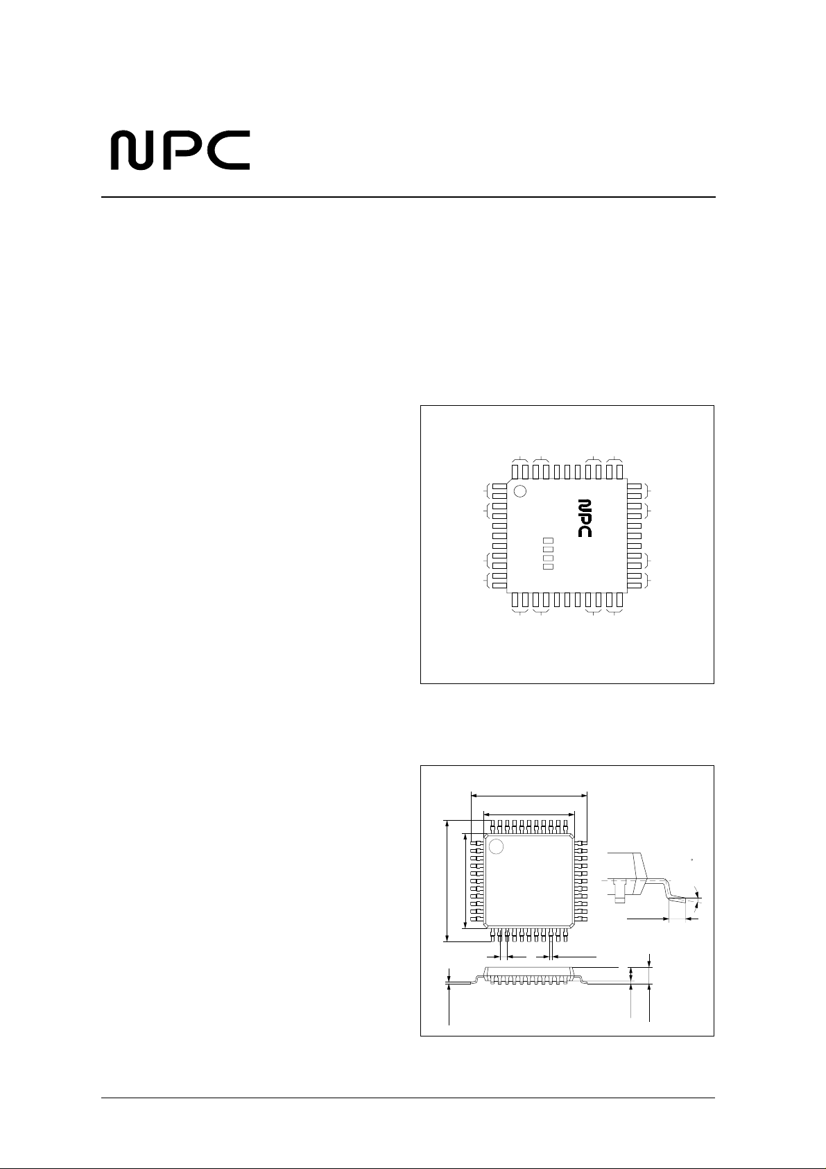
The SM5844AF operates from a 5 V supply, and is
available in 44-pin QFPs.
FEATURES
Functions
■
Left/right-channel processing (stereo)
Input sample rate (fsi) ranges
■
• 24 to 48 kHz (256fsi mode)
• 27 to 55 kHz (384fsi mode)
Output sample rate (fso) range
■
• 20 to 100 kHz
Sample rate conversion ratio (fso/fsi)
■
• 0.5 to 2.0 times
Asynchronous input and output timing (clock
■
inputs)
System clock inputs (input and output clocks
■
independent)
• 256fsi or 384fsi input system clock
• 256fso or 384fso output system clock
Deemphasis filter
■
• IIR-type filter
• 44.1, 48 or 32 kHz
Digital attenuator
■
• 11-bit data for 1025 levels
• Smooth, incremental attenuation change
• +12 dB gain shift function
Direct mute function
■
Through mode operation
■
• Input to output direct
Output data clocks (LRCO, BCKO)
■
• External input (slave mode)
• Output system clock generated internally
(master mode)
CMOS-level input/outputs
■
5 V (standard) single supply
■
44-pin QFP
■
Molybdenum-gate CMOS process
■
APPLICATIONS
■
Digital audio equipment, sample rate conversion
(audiovisual amplifiers, CD-R, DAT, MD and 8
mm VTRs)
■
Commercial recording/editing equipment, sample
rate conversion
■
Input data jitter elimination
PINOUT
THRUN
OCKSL
MDT/FSI2
MLEN/DEEM
SLAVE
OW18N
VSS
RSTN
TST2N
TST1N
STATE
IISN
OW20N
BCKI
ICKSL
IFM1
IFM2
DI
LRCI
ICLK
DOUT
VDD
BCKO
DMUTE
OCLK
LRCO
SM5844AF
MCOM
MDT/FSI1
PACKAGE DIMENSIONS
Unit: mm
44-pin QFP
+
12.80 0.30
-
10.00
-
+
10.00
12.80 0.30
+
0.60 0.20
-
+
0.35 0.10
-
1.45
0 to 0.20
1.75MAX
+
0.80
-
0.17 0.05
0 to 10
NIPPON PRECISION CIRCUITS—1
Page 2
SM5844AF
Filter Characteristics and Converter
Efficiency
20-bit internal data word length
■
Deemphasis filter characteristics (IIR filter)
■
• ±0.03 dB gain deviation from ideal filter
characteristics
Converter noise levels
■
• ≤ − 110 dB internally-generated noise
• − 98 dB (16-bit output), − 110 dB (18-bit output)
and − 122 dB (20-bit output) word rounding
noise
■
Anti-aliasing LPF characteristics (4 FIR filters)
with automatic output/input sample rate
conversion ratio selection
• Up converter LPF (1.0 to 2.0 times)
• Down converter LPF 1 (48.0 to 44.1 kHz or
0.92 times)
• Down converter LPF 2 (44.1 to 32.0 kHz or
0.73 times)
• Down converter LPF 3 (48.0 to 32.0 kHz or
0.67 times)
■
Output S/N ratio (theoretical values)
Output signal word
length
16 bits 94.8 dB 97 dB
18 bits 97.5 dB 106 dB
20 bits 97.7 dB 109 dB
16-bit input word
length
S/N ratio
20-bit input word
length
Interfaces
■
Input data format
• 2s-complement, L/R alternating, serial
• Normal format (non IIS)
Mode Word length
1 16 bits
20 bits3 Front
4 Rear LSB first
■
Output data format
Front/rear
packing
Rear
• 2s-complement, MSB first, L/R alternating,
serial
• Continuous bit clock
Mode Word length IIS selection
1 16 bits
Nor mal (non
3 20 bits
4 20 bits
5 16 bits
7 20 bits
IIS)
IIS6 18 bits
Data
sequence
MSB first2
Front/rear
packing
Rear2 18 bits
Front
NIPPON PRECISION CIRCUITS—2
Page 3
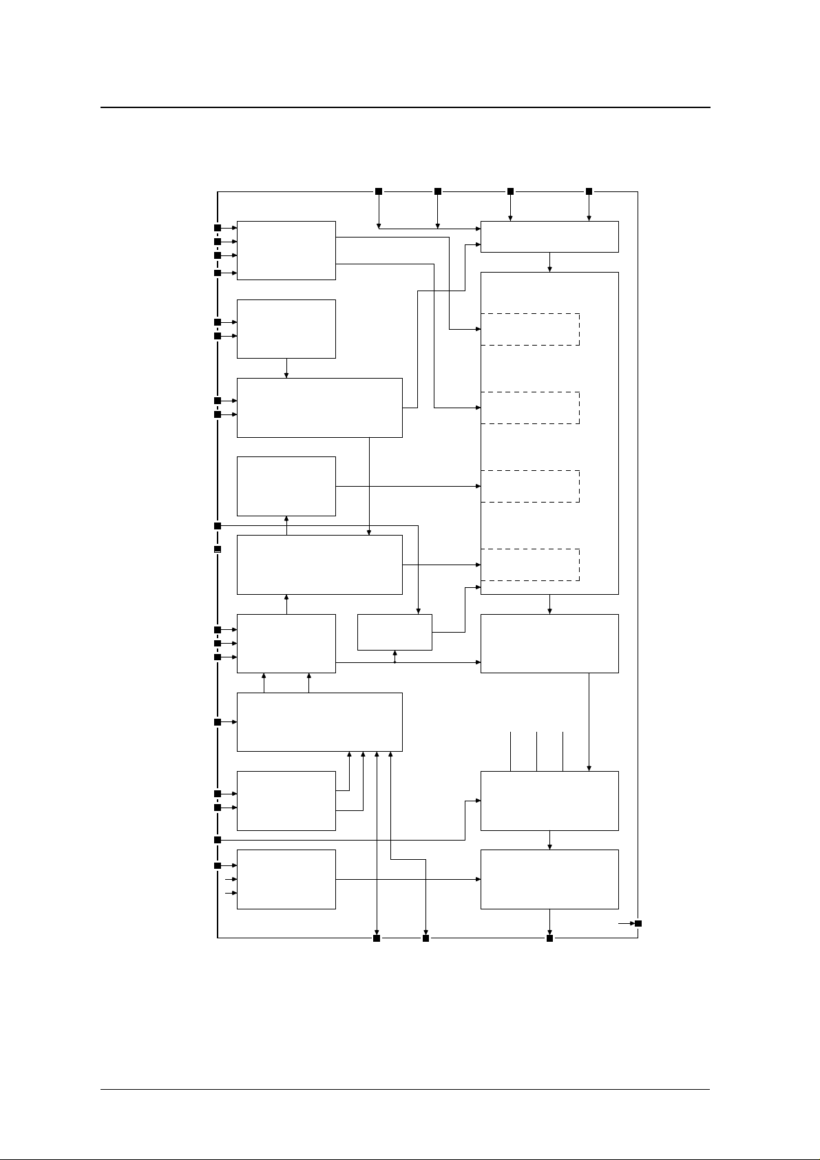
BLOCK DIAGRAM
SM5844AF
IFM1 IFM2 BCKI DI
MCOM
MDT/FSI1
MCK/FSI2
MLEN/DEEM
ICLK
ICKSL
LRCI
RSTN
TST1N
TST2N
Deemphasis and
attenuator setup
Input-stage
divider
Input timing
controller
Filter characteristic
select
Output operation
timing controller
Input data
interface
Arithmetic
operations
Deemphasis
operation
Attenuator
Interpolation
filter operation
Output
operation
OW18N
OW20N
IISN
SLAVE
OCLK
OCKSL
THRUN
DMUTE
Output format
controller
Output-stage
clock select
Output-stage
divider
Mute
generator
Dither
LRCO BCKO DOUT
Output data
interface
LRCI BCKI DI
Through mode
switching
Direct mute
STATE
NIPPON PRECISION CIRCUITS—3
Page 4
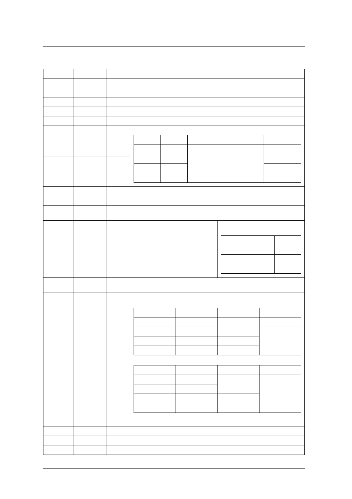
PIN DESCRIPTION
SM5844AF
1
Number
1, 2 DI Ip Data input
3, 4 BCKI Ip Input bit clock
5 LRCI
6 ICLK I Input system clock input
7 ICKSL Ip Input system clock (ICLK) select. 384fsi when HIGH, and 256fsi when LOW .
8, 9 IFM1 Ip
10, 11 IFM2 Ip
12, 13 V DD – 5 V supply pin
14, 15 DMUTE Ip Direct mute pin
16 MCOM Ip
17 MDT/FSI1 Ip
18 MCK/FSI2 Ip
Name I/O
3
2
Ip Input word clock (fsi)
Input format select
IFM1 IFM2 W ord length Data sequence Data position
L O W L O W 16 bits
LOW HIGH
HIGH HIGH LSB first Rear packed
Interface switch control pin. M D T, MCK and MLEN control when HIGH. FSI1, FSI2 and DEEM
control when LOW.
When MCOM is HIGH: Microcontroller interface
data input (MDT)
When MCOM is HIGH: Microcontroller interface
bit clock (MCK)
Description
MSB first
20 bitsHIGH LOW Front packed
When MCOM is LOW: Deemphasis frequency
set pins
FSI1 FSI2 fsi
LOW HIGH 48.0 kHz
×
HIGH HIGH 32.0 kHz
Rear packed
LO W 44.1 kHz
19, 20 MLEN/DEEM Ip
21, 22 OW18N Ip
23, 24 OW20N Ip
25, 26 IISN Ip IIS output mode select. Normal mode when HIGH, and IIS mode when LOW .
27 S TAT E O Internal operation status output (for operation check)
28 TST1N Ip Output dither control. Dither ON when LOW, and OFF when HIGH.
29 TST2N Ip Test pin. Test mode when LOW. Normal operating mode when HIGH.
When MCOM is HIGH: Microcontroller data word latch clock (MLEN)
When MCOM is LOW: Deemphasis ON/OFF control (DEEM)
Output format select
When IISN = HIGH (normal mode)
OW20N OW18N Word length Data position
LOW LOW
20 bits
LOW HIGH
HIGH HIGH 16 bits
When IISN = LOW (IIS mode)
OW20N OW18N Word length Data position
LOW LOW
20 bits
LOW HIGH
HIGH LOW 18 bits
HIGH HIGH 16 bits
Front packed
Rear packedHIGH LOW 18 bits
IIS mode
Front packed
NIPPON PRECISION CIRCUITS—4
Page 5
+
−
−
−
°
°
−
°
SM5844AF
Number
1
Name I/O
2
Description
30, 31 RSTN Ip Reset pin
32, 33 VS S – 0 V ground pin
34, 35 SL AV E Ip
BC KO and LRCO mode set. Outputs (master mode) when LOW, and inputs (slave mode) when
HIGH.
36, 37 T H RUN Ip DOUT through mode set. Normal mode when HIGH, and through mode when LOW.
38 OCKSL Ip Output system clock (OCLK) select. 384fso when HIGH, and 256fso when LOW .
39 OCLK I Output system clock input
40 LRCO
3
I/O Output word clock input/output (fso). Input/output mode set by the level on SLAV E.
41, 42 B C K O I/O Output bit clock input/output. Input/output mode set by the level o n S LAVE .
43, 44 DOUT O Data output
1. Pins which have the same name are connected internally. Accordingly, circuit connections can be made to either pin or to both pins.
2. I = input, Ip = Input with pull-up resistor (HIGH-level pins can be left open), O = output, I/O = input/output
3. fsi is the input word clock (LRCI) frequency, and fso is the output word clock (LRCO) frequency.
SPECIFICATIONS
Absolute Maximum Ratings
V
= 0 V
SS
Parameter Symbol Rating Unit
Supply voltage range V
Input voltage range V
Storage temperature range T
Po w er dissipation P
Soldering temperature T
Soldering time t
DD
IN
stg
D
sld
sld
0.3 to 7.0 V
0.3 to V
0.3 V
DD
40 to 125
550 m W
255
10 s
C
C
Recommended Operating Conditions
V
= 0 V
SS
Parameter Symbol Rating Unit
Supply voltage range V
Operating temperature range T
DD
opr
4.75 to 5.5 V
20 to 70
C
NIPPON PRECISION CIRCUITS—5
Page 6
DC Electrical Characteristics
−
V
= 4.75 to 5.5 V, V
DD
= 0 V, T
SS
= − 20 to 70 ° C
a
SM5844AF
−
Ω
Parameter Symbol Condition
Current consumption I
HIGH-level input voltage
L O W -level input voltage
AC-coupled input voltage
HIGH-level output voltage
L O W-level output voltage
HIGH-level input current
L O W -level input current
Input leakage current
Pull-up resistance
1. ICKSL = LOW, OCKSL = LOW, f
2. Pins ICLK and OCLK.
2,3
2,3
2
4
4
2
2,3
3
3
= 13.0 MHz, f
ICLK
min typ max
DD
V
IH
V
IL
V
ACI
V
OH
V
OL
I
IH
I
IL
I
LH
R
IH
V
DD
I
OH
I
OL
V
IN
V
IN
V
IN
= 13.0 MHz, no output load
OCLK
1
= 5.0 V
––80mA
0.7V
DD
– – 0.3V
0.3V
DD
=
1.0 mA V
DD
= 1.0 mA – – 0.4 V
= V
DD
–1020µA
= 0 V – 1 0 2 0 µA
= V
DD
– – 1.0 µ A
250 500 1000 k
Rating
Unit
––V
DD
––V
0.5 – – V
V
p-p
3. Pins DI, BCKI, LRCI, ICKSL, IFM1, IFM2, DMUTE, MCOM, MDT/FSI1, MCK/FSI2, MLEN/DEEM, OW18N, OW20N, IISN, TST1N, TST2N, RSTN,
TH RUN, OCKSL and SLAVE.
4. Pins DOUT, BCKO, LRCO and STATE.
AC Electrical Characteristics
V
= 4.75 to 5.5 V, V
DD
ICLK input
= 0 V, T
SS
= − 20 to 70 ° C
a
Parameter Symbol
L O W -level clock
pulsewidth
HIGH-level clock
pulsewidth
Clock pulse cycle t
OCLK input
Parameter Symbol
L O W -level clock
pulsewidth
HIGH-level clock
pulsewidth
Clock pulse cycle t
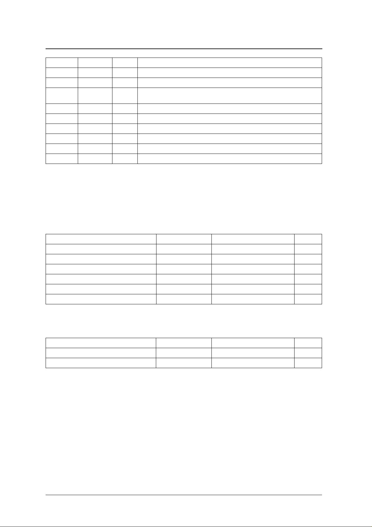
ICLK and OCLK timing
ICLK
OCLK
t
CWL
t
CWH
CY
t
CWL
t
CWH
CY
Condition Rating
ICKSL System clock min typ m ax
L OW 256fsi 30 – –
HIGH 384fsi 10 – –
L OW 256fsi 30 – –
HIGH 384fsi 10 – –
L OW 256fsi 80 – 162
HIGH 384fsi 47 – 106
Condition Rating
OCKSL System clock min typ m ax
LO W 256fso 15 – –
HIGH 384fso 10 – –
LO W 256fso 15 – –
HIGH 384fso 10 – –
LO W 256fso 39 – 200
HIGH 384fso 26 – 130
t
CWH
t
CY
t
CWL
Unit
ns
ns
ns
Unit
ns
ns
ns
>0.7V
0.5V
<0.3V
DD
DD
DD
NIPPON PRECISION CIRCUITS—6
Page 7
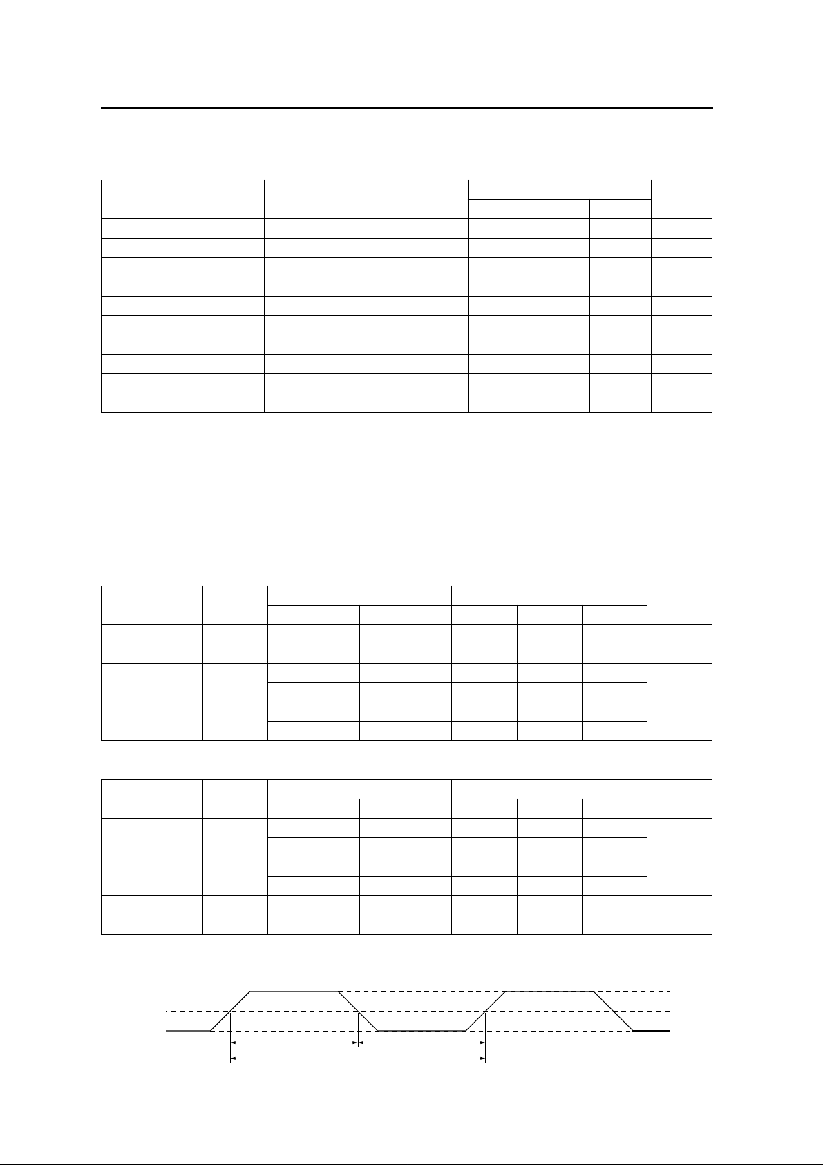
BCKI, DI, LRCI inputs
SM5844AF
Parameter Symbol
BCKI LOW-level pulsewidth t
BCKI HIGH-level pulsewidth t
BCKI pulse cycle t
DI setup time t
DI hold time t
Last BCKI rising edge to LRCI edge t
LRCI edge to first BCKI rising edge t
BCKI, DI, LRCI timing
BCKI
t
DS
DI
BCWL1
BCWH1
BCY1
DS
DH
BL1
LB1
Rating
min typ max
50 – – ns
50 – – ns
100 – – ns
50 – – ns
50 – – ns
50 – – ns
50 – – ns
t
BCY1
t
BCWH1
t
DH
t
BCWL1
Unit
0.5V
0.5V
DD
DD
t
BL1
LRCI
BCKO, LRCO (Inputs when SLAVE = HIGH)
Parameter Symbol
B CK O L OW -level pulsewidth t
BC KO HIGH-level pulsewidth t
B C KO pulse cycle
1
Last BCKO rising edge to LRCO edge t
LRCO edge to first BCKO rising edge t
BCWL2
BCWH2
t
BCY2
BL2
LB2
1. BCK O clock inputs exceeding 64fso cannot be detected, and will cause incorrect operation.
min typ max
78 – – ns
78 – – ns
156 – – ns
78 – – ns
78 – – ns
Rating
t
LB1
0.5V
DD
Unit
NIPPON PRECISION CIRCUITS—7
Page 8
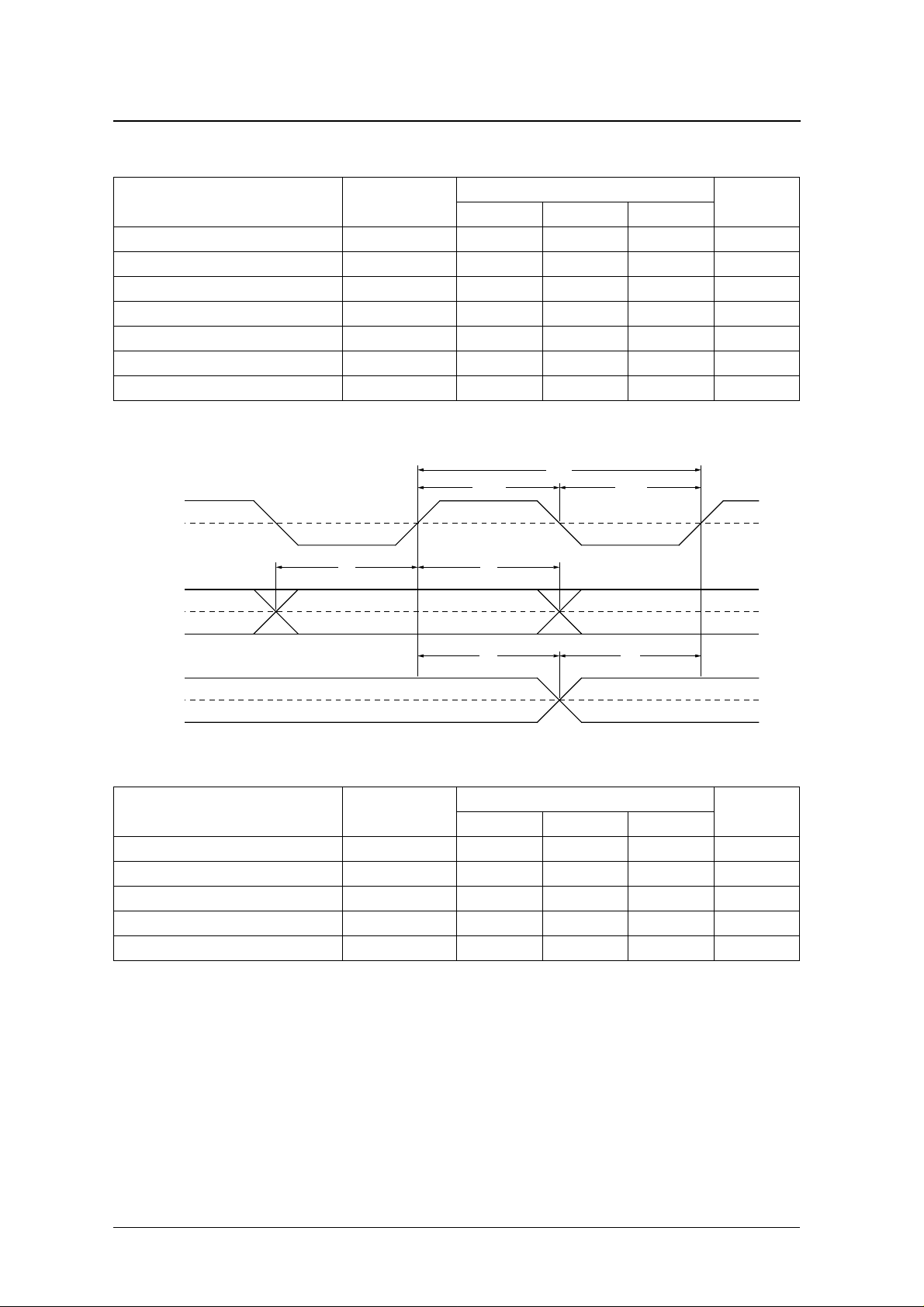
BCKO, LRCO timing
SM5844AF
t
BCWH2
t
BCY2
t
BCWL2
BCKO
t
BL2
LRCO
MDT, MCK, MLEN inputs
Parameter Symbol
MCK and MLEN rise time
MCK and MLEN fall time
MDT setup time t
MDT hold time t
MLEN setup time t
MLEN hold time t
MLEN LOW-level pulsewidth t
MLEN HIGH-level pulsewidth t
1
1
t
r
t
f
MDS
MDH
MCS
MCH
MEWL
MEWH
1. tr and tf are the input waveform transition times measured between 0.1VDD and 0.9VDD levels.
min typ max
– – 100 ns
– – 100 ns
50 – – ns
50 – – ns
50 – – ns
50 – – ns
50 – – ns
50 – – ns
Rating
0.5V
DD
t
LB2
0.5V
DD
Unit
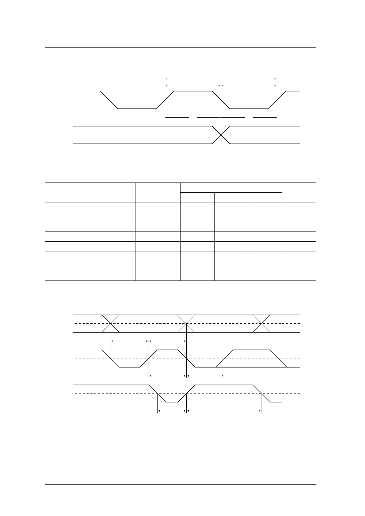
MDT, MCK, MLEN timing
MDT
MCK
MLEN
t
MDS
t
MDH
t
MCS
t
MEWL
t
MCH
t
MEWH
0.5V
0.5V
0.5V
DD
DD
DD
NIPPON PRECISION CIRCUITS—8
Page 9

DEEM, DMUTE inputs
SM5844AF
Parameter Symbol
Rise time t
Fall time t
DOUT, BCKO, LRCO input/outputs
SLAVE = LOW (outputs), CL = 15 pF
Parameter Symbol Condition
LRCO pulse cycle t
LRCO LOW-level pulsewidth t
LRCO HIGH-level pulsewidth t
B C KO pulse cycle t
B CK O L OW -level pulsewidth t
BC KO HIGH-level pulsewidth t
OCLK to BCKO delay time
(OCKSL = LOW)
OCLK to BCKO delay time
(OCKSL = HIGH)
BC KO to DOUT and LRCO delay
time
LOCY
LOCL
LOCH
BOCY
BOWL
BOWH
t
sbH1
t
sbL1
t
sbH2
t
sbL2
t
bdH1
t
bdL1
Rating
min typ max
r
f
– – 100 ns
– – 100 ns
Rating
min typ max
– 1/fso – ns
– 1/2fso – ns
– 1/2fso – ns
OCKSL = LOW – 1/64fso –
OCKSL = HIGH – 1/48fso –
OCKSL = LOW – 1/128fso –
OCKSL = HIGH – 1/96fso –
OCKSL = LOW – 1/128fso –
OCKSL = HIGH – 1/96fso –
From OCLK fall to BCKO
rise
From OCLK fall to BCKO
fall
From OCLK fall to BCKO
rise
From OCLK fall to BCKO
fall
From BCKO fall to DOUT
rise
From BCKO fall to DOUT
fall
10–70ns
10–70ns
15–80ns
15–80ns
0–20ns
0–20ns
Unit
Unit
ns
ns
ns
SLAVE = HIGH (inputs), CL = 15 pF
Parameter Symbol Condition
t
bdH2
BC KO to DOUT delay time
t
bdL2
From BCKO fall to DOUT
rise
From BCKO fall to DOUT
fall
Rating
Unit
min typ max
10 – 100 ns
10 – 100 ns
NIPPON PRECISION CIRCUITS—9
Page 10

DOUT, BCKO, LRCO timing
OCLK
BCKO
SM5844AF
BCKO
DOUT
LRCO
t , t
sbL1 sbL2
t , t
bdH bdL
t
bdH
t
BOWH
t
LOCH
t
BOCY
t
LROOY
t , t
sbH1 sbH2
t
bdL
t
BOWL
t
LOCL
NIPPON PRECISION CIRCUITS—10
Page 11

Filter Characteristics
Anti-aliasing filter frequency characteristic
0
SM5844AF
20
40
60
80
Attenuation (dB)
100
120
140
0.250 0.300 0.350 0.400 0.450 0.500 0.550 0.600 0.650
48k 32k
48k 44.1k
44.1k 32k
Up conversion
Frequency (fs)
Deemphasis filter frequency characteristic
0
2
4
48.0 kHz
44.1 kHz
32 kHz
0
Θ
–20
–40
6
Attenuation (dB)
8
10
12
10 20 50 100 200 500 1k 2K 5k 10k 20k
Phase Attenuation
Frequency (Hz)
48.0, 44.1 and 32 kHz
Phase characteristic, (°)
–60
NIPPON PRECISION CIRCUITS—11
Page 12

SM5844AF
FUNCTIONAL DESCRIPTION
Input Data Interface (DI, LRCI, BCKI, IFM1, IFM2)
Mode IFM1 IFM2 W ord length Data position
1 LO W L O W 16 bits
2 LOW HIGH
20 bits3 HIGH LOW Front packed
4 HIGH HIGH Rear packed LSB first
Rear packed
Attenuator and Deemphasis Selection
The attenuator is set using the microcontroller
interface. When the attenuator is used, deemphasis
settings also need to be set using the microcontroller
interface. The microcontroller interface comprises
MDT, MCK and MLEN, and is used to receive all
input serial data.
Table 1. Attenuator and deemphasis function
selection
Function set method
Function
Deemphasis
ON/OFF
External pins
(MCOM = LOW)
DEEM FDEEM
Microcontroller
interface flags
(MCOM = HIGH)
Data
sequence
MSB first
Common features
Non IIS
L/R alternating
Bit serial
Deemphasis
frequency (fsi)
select
Attenuator data set N/A (no attenuation) 11 bits (a1 to a11)
Test mode select
FSI1, FSI2 FFSI1, FFSI2
Irreversible
(test mode 1)
FTST1, FTST2
When MCOM is HIGH, serial data received on
MDT , MCK and MLEN sets the attenuation data and
control flag data.
When MCOM is LOW, the logic levels on FSI1,
FSI2 and DEEM select the device function.
NIPPON PRECISION CIRCUITS—12
Page 13

SM5844AF
Microcontroller Interface (MCOM, MDT, MCK, MLEN)
When MCOM is HIGH, MDT (data), MCK (clock)
and MLEN (latch enable clock) interface pins are
used.
Input data on MDT is synchronized to the MCK
clock. Data is read into the input stage shift register
on the rising edge of MCK. Accordingly, the input
data should change on the falling edge of MCK.
Input data enters an internal SIPO (serial-to-parallel
converter register), and then the parallel data is
B2
B3
MDT
MCK
MLEN
LOWB1a0
MSB
a1
Figure 1. Attenuation data format (B1 = LOW)
latched into the mode register on the rising edge of
the latch enable clock MLEN.
The mode register addressed is determined by the 1st
bit of the 12 data bits before MLEN goes HIGH. If
this bit is LOW, then the data is read into the
attenuation data register as shown in figure 1. If this
bit is HIGH, then the data is read into the mode flag
register as shown in figure 2. The function of each bit
in the mode flag register is described in table 1.
B4
a2
B8
a6
B9a8B10
a7
MCK and MLEN can also follow the dotted lines.
B11
a9
B12
a10
LSB
MDT
MCK
MLEN
B1 B2
HIGH
B5
Not used
B6
FTST1
FTST2
FRATEB8F12DBB9FFSI1
Figure 2. Mode flag data format (B1 = HIGH)
B10
MCK and MLEN can also follow the dotted lines.
B11
FFSI2
B12* * B7
FDEEM
NIPPON PRECISION CIRCUITS—13
Page 14

Table 2. Mode flag description
SM5844AF
B1 Bit Mode flag
B2 to B5 Not used
B6 FTST1 Test mode select 1
B7 FTST2 Test mode select 2 LOW
B8 FR AT E Input/output rat e
HIGH
B9 F12DB Attenuator
B10 FFSI1
B11 FFSI2
Mode function select
Parameter LOW/HIGH Select
TST2N = LOW
FTST2 FTST1 Mode
LOW LOW 0
LOW HIGH 1
HIGH LOW 2
HIGH HIGH 3
LOW
HIGH
LO W Nor mal operation (no shift)
HIGH +12 dB gain shift
Deemphasis filter fs
select 1
Deemphasis filter fs
select 2
Input/output sample rate ratio check after eve ry
output
Input/output sample rate ratio check for high
accuracy after every 2048 outputs
FFSI2 FFSI1 fsi
LOW LOW
LOW HIGH
HIGH LOW 48.0 kHz
HIGH HIGH 32.0 kHz
Reset
mode
LOW
LOW
LOW
LOW
44.1 kHz
LOW
B12 FDEEM
Deemphasis control
ON/OFF
LOW Deemphasis filter OFF
HIGH Deemphasis filter ON
Deemphasis (DEEM, FSI1, FSI2 pins or FDEEM, FFSI1, FFSI2 flags)
The digital deemphasis filter is an IIR filter with variable coefficients to faithfully reproduce the gain and
phase characteristics of standard analog deemphasis
filters.
The filter coefficients are selected by FSI1 (or FFSI1
flag) and FSI2 (or FFSI2 flag) to correspond to the
sampling frequencies fs = 44.1, 48.0 and 32.0 kHz.
Table 3. Deemphasis ON/OFF
When MCOM = LOW When MCOM = HIGH Deemphasis
DEEM = HIGH FDEEM = HIGH O N
DEEM = LOW FDEEM = LOW OFF
Table 4. Deemphasis fs select (FSI1, FSI2 pins or
FFSI1, FFSI2 flags)
MCOM = LOW (MCOM = HIGH)
FSI1 (FFSI1) FSI2 (FFSI2)
LOW LOW
HIGH L OW
LOW HIGH 48.0 kHz
HIGH HIGH 32.0 kHz
LOW
fs
44.1 kHz
NIPPON PRECISION CIRCUITS—14
Page 15

Attenuation (MDT, MCK, MLEN)
SM5844AF
The digital attenuator coefficients are read in as
serial data on the microcontroller interface. Data on
MDT is read into the internal shift register on the
rising edge of MCK, and then 12 bits are latched
internally on the rising edge of MLEN.
B2
B3
MDT
MCK
MLEN
LOWB1a0
MSB
a1
Figure 3. Attenuation data format (microcontroller interface)
Although the attenuation data comprises 11 bits,
only 1025 levels are valid as given by the following.
10
DATT ai2
=
∑
i 0=
10 i–()
×
The gain of the attenuator for values of DATT from
001H to 400H are given by the following equations.
Note that when the F12DB flag is HIGH, the gain is
shifted by +12.0412 dB.
When the leading bit is 0 (B1 = LOW), the following
11 bits are read into the attenuation register and used
as an unsigned integer in MSB first format. See
figure 3.
B4
a2
B8
a6
Gain 20
B9a8B10
a7
MCK and MLEN can also follow the dotted lines.
DATT
--------------- -
log× [dB]=
1024
B11
B12
a9
a10
LSB
when F12DB = LOW
DATT
20
when F12DB = HIGH
--------------- -
log× [dB]=
256
−∞
−∞
−
−
−
−
After a system reset initialization, DATT is set to
400H and the F12DB flag is LOW, corresponding to
0 dB gain. (The F12DB flag is described in table 2.)
Table 5. Attenuator settings
Attenuation data DATT
000H
001H
↓↓↓↓↓
100H
↓↓↓↓↓
3FFH
400H (to 7FFH) 0 1.0 12.041 4.0
F12DB = LOW (default) F12DB = HIGH
Gain (dB) Linear expression Gain (dB) Linear expression
0.0
60.206 1/1024
12.041 256/1024 0.0 256/256
0.0085 1023/1024 12.032 1023/256
48.165 1/256
NIPPON PRECISION CIRCUITS—15
0.0
Page 16

SM5844AF
Attenuator operation
A change in the attenuation data DATT causes the
gain to change smoothly from its previous value
towards the new setting. The new attenuation data is
stored in the attenuation data register and the current
attenuation level is stored in a temporary register.
Consequently, if a new attenuation level is read in
before the previously set level is reached, the gain
changes smoothly from the current value towards the
latest setting as shown in figure 4.
The attenuation counter output changes, and hence
the gain changes, by 1 step every output sample. The
time taken to reduce the gain from 0 dB (or 12 dB) to
dB is (1024/fso), which corresponds to
approximately 23.2 ms when fso = 44.1 kHz.
Level 1
0 dB
Gain
Level 2
− ∞
∆t
Level 3
Level 4
Figure 4. Attenuator operation example
Level 5
Time
−∞
NIPPON PRECISION CIRCUITS—16
Page 17

Direct Mute (DMUTE)
Direct mute ON/OFF
Table 6. DMUTE operation
DMUTE Function
Nor mal data is output from the next output word (mute
LOW
OFF)
HIGH 0 data is output from the next output word (mute ON)
Reset mute
Table 7. RSTN mute operation
RSTN Function
L OW 0 data is output from the next output word (mute ON)
SM5844AF
HIGH
Nor mal data is output from the 3073rd output word
(mute OFF)
Internal operating status (STATE)
Internally, all functions are performed using 20-bit
serial data, and the conversion rate and filter type are
Table 8. Bit function
Output bit position Content
(Output data cycle/input data cycle)
Ex.
1st to 18th
19th DA1 Selected filter type
20th DA0
1st 18th
00.1111111111110111 ⇒ 1.0 times
01.1111111111110111 ⇒ 2.0 times (1/2 conversion rate ratio)
00.0111111111110111 ⇒ 0.5 times (2.0 conversion rate ratio)
9
D A 1 D A 0 Filter Mode
0 0 Up converter 1
1 0 44.1 to 48 kHz 2
0 1 32 to 44.1 kHz 3
1 1 32 to 48 kHz 4
automatically selected for output. Output data is in
20-bit front-packed format.
−
Note that when THRUN is LOW, LRCO and BCKO are not guaranteed to be synchronized to the STATE
output.
NIPPON PRECISION CIRCUITS—17
Page 18

System Clock
SM5844AF
Input system clock (ICLK, ICKSL)
The input system clock can be set to run at either
256fsi or 384fsi, where fsi is the input frequency on
LRCI.
Note that ICLK and LRCI should be divided from a
common clock source or PLL to maintain
synchronism.
Output system clock (OCLK, OCKSL)
The output system clock can be set to run at either
256fso or 384fso, where fso is the input frequency on
LRCO. In through mode, OCLK and OCKSL have
no function and are not used.
Note that in slave mode, a suitable clock must be
input on OCLK. The clock on OCLK should ideally
have a protection circuit to prevent incorrect
Table 9. ICLK system clock
ICKSL ICLK system clock rate
HIGH 384fsi
L OW 256fsi
operation for times when the clock on ICLK is
halted.
Table 10. OCLK system clock
SLAVE OCKSL OCLK system clock rate
LOW
HIGH
HIGH 384fso
LO W 256fso
Not used
Output data interface and output clock selection (LRCO, BCKO, DOUT, SLAVE)
Table 11. Output mode description
THRUN SLAVE
Mode Description LRCO, BCKO state
Function
LOW Master mode
HIGH
HIGH Slave mode
LOW
1. The number of BCKO input clock cycles should not exceed 64 per word. Correct operation is not guaranteed beyond these limits.
Through mode
System Reset (RSTN)
At power-ON, all de vice functions must be reset. The
Output word clock (LRCO) and output bit clock
(B CKO) are divided from OCLK.
Output word clock (LRCO) and output bit clock
(BCKO) are supplied exter nally.
Output word clock (LRCO), output bit clock
(BCKO) and output data (DOUT) are the
same as LRCI, BCKI and DI, respectively.
Through Mode (THRUN)
Table 12. THRUN operation
device is reset by applying a LOW-level pulse on
RSTN. At system reset, the internal arithmetic
operation, output timing counter and internal flag
register operation are synchronized on the next LRCI
rising edge. Note that all flags are set to their defaults
(all LOW).
THRUN Mode Description
LOW Through mode
HIGH Normal mode Sample rate converter operation
Direct connections are made: LRCI
to LRCO, BCKI to BCKO , and DI to
DOUT.
A power-ON reset signal can be applied from an
external microcontroller. For systems where ICLK
and LRCI are stable at power ON, initialization can
be performed by connecting a 0.001 µF capacitor
between RSTN and VSS. Otherwise, a capacitor
value should be chosen such that RSTN does not go
HIGH until after LRCI and ICLK have stabilized.
Outputs
1
Inputs
Outputs
×
×
NIPPON PRECISION CIRCUITS—18
Page 19

SM5844AF
Internal Arithmetic Timing Auto-reset
The clock on LRCI should pass through 1 cycle for
every 384 (ICKSL = HIGH) or 256 (ICKSL = LOW)
ICLK clock cycles to maintain correct internal
arithmetic sequence. If the number of ICLK cycles is
different, increases or decreases, or any jitter is
present, device operation could be affected.
There is a fixed-value tolerance within which the
internal sequence and LRCI clock timing are not
adversely affected.
Table 13. Clock tolerance
ICKSL Allowa b le clock variation
HIGH (384fs mode) +8/−6 cycles
LO W (256fs mode) +4/−3 cycles
Whenever the allowable tolerance is exceeded, the
internal sequence is automatically reset so that the
internal sequence matches the LRCI clock. When
this occurs, there is a possibility that click noise will
be generated.
Output Timing Calculation
The output timing is calculated to maintain the
desired ratio between the output data cycle and the
input data cycle.
Filter Characteristic Selection
Conversion rates from 0.5 to 2.0 times are supported
using the following 4 filter types.
The ratio between the output sample rate and input
sample rate is measured automatically and the most
suitable filter type for this ratio is selected
automatically.
Table 15. fs ratio and filter selection
Mode Filter fs ratio (fso/fsi) Selects range
1 U p c on ver ter 1.0 to 2.0 ≥ 0.97
2 48.0 to 44.1 kHz 0.91875 0.865 to 0.97
3 44.1 to 32.0 kHz 0.72562 0.711 to 0.865
4 48.0 to 32.0 kHz 0.66667 ≤ 0.711
Output Format Control (OW18N,
OW20N, IISN)
The output is in MSB-first, 2s-complement, L/R
alternating, bit serial format with a continuous bit
clock.
Table 14. Output format selection
Inputs Output for mat
Mode
IISN O W20N OW18N
1
3 LOW HIGH 20 bits
4 LOW L O W 20 bits
5
7LOW
HIGH HIGH 16 bits
HIGH
HIGH HIGH 16 bits
LOW
Word
length
×
20 bits
IIS
selection
Non IIS
IIS6 HIGH LOW 18 bits
Front/rear
packing
Rear2 HIGH LOW 18 bits
Front
When the selected fs conversion ratio and the actual
sample rate conversion ratio do not coincide, the
following phenomenon are generated.
Table 16. fs ratio mismatch
Condition Affect
Actual sample rate conversion
ratio is low er than the selected
filter conversion ratio
Actual sample rate conversion
ratio is higher than the selected
filter conversion ratio
Note: An output noise may be generated if the fs conversion ratio
changes at a rate greater than 0.057%/sec.
The audio band high-pass
develops aliasing noise.
The audio band high-pass is cut
off.
NIPPON PRECISION CIRCUITS—19
Page 20

SM5844AF
TIMING DIAGRAMS
Input Timing Examples (DI, BCKI, LRCI)
Audio data input timing (rear-packed 16-bit word, IFM1 = LOW, IFM2 = LOW)
1/fs
BCKI
LRCI
MSB LSB MSB LSB
DI
Left-channel data Right-channel data
Audio data input timing (rear-packed 20-bit word, IFM1 = LOW, IFM2 = HIGH)
1/fs
BCKI
LRCI
MSB LSB MSB LSB
DI
Left-channel data Right-channel data
1615142116151421
2019182120191821
Audio data input timing (front-packed 20-bit word, IFM1 = HIGH, IFM2 = LOW)
1/fs
MSB LSB
Right-channel data
BCKI
LRCI
MSB LSB
DI
Left-channel data
1 2 3 19 20 1 2 3 19 20
All data bits after the LSB (20th bit) are ignored. Accordingly, more than 20 BCKI cycles are required.
1
NIPPON PRECISION CIRCUITS—20
Page 21

SM5844AF
Audio data input timing (rear-packed 20-bit word, LSB first, IFM1 = HIGH, IFM2 = HIGH)
LSB MSB LSB MSB
DI
BCKI
LRCI
Left-channel data Right-channel data
Output Timing Examples (DOUT, BCKO, LRCO)
Audio data output timing (rear-packed 16-bit word)
MSB LSB
DOUT
BCKO
Left-channel data
21 15 16
1/fs
1/fso
MSB LSB
21 15 16
Right-channel data
2019182120191821
LRCO
Audio data output timing (rear-packed 18-bit word)
MSB LSB
DOUT
BCKO
LRCO
Left-channel data
21 17 18
Audio data output timing (rear-packed 20-bit word)
MSB LSB
DOUT
Left-channel data
21 19 20
1/fso
MSB LSB
21 17 18
1/fso
MSB LSB
21 19 20
Right-channel data
Right-channel data
BCKO
LRCO
NIPPON PRECISION CIRCUITS—21
Page 22

SM5844AF
Audio data output timing (front-packed 20-bit word, OW18N = LOW, OW20N = LOW)
1/fso
DOUT
BCKO
LRCO
MSB LSB
Left-channel data
21
19 20
MSB
21
Right-channel data
LSB
19 20
Audio data output timing (IIS mode, front-packed 16/18/20-bit word selected by OW18N and
OW20N)
1/fso
DOUT
MSB LSB
Left-channel data
21 16 17 18 19 20
MSB LSB
Right-channel data
21 16 17 18 19 20
BCKO
LRCO
Data is output in 20-bit units.
State Data Output Timing
State data output timing (IISN = HIGH)
MSB LSB
STATE
BCKO
LRCO
State data output timing (IISN = LOW)
MSB LSB
STATE
State data
21
State data
21
1/fso
19 20
1/fso
19 20
BCKO
LRCO
NIPPON PRECISION CIRCUITS—22
Page 23

SM5844AF
Delay Time
t
is the time when the serial input data has been
INPUT
read in completely (on the rising edge of LRCI).
t
OUTPUT
is the time when the serial output data has
1/fs
LRCI
Serial data input
t
input
LRCO
1/fso
t
INPUT
t – t
OUTPUT INPUT
been read out completely (on the rising edge of
LRCO). The delay between input and output is given
49 ±2
by t
OUTPUT
− t
INPUT
Serial data output
= (49 ± 2)/fsi.
t
output
t
OUTPUT
NIPPON PRECISION CIRCUITS—23
Page 24

TYPICAL APPLICATIONS
Input Interface Circuits
Digital audio interface receiver (PD0052)
SM5844AF
384fs
LRCK
BCK
DATA
MODE
EMP
32k
VCOOUT
DIR
PD0052
44.1k 48k
Digital audio interface transceiver(YM3613)
SM5844AF
OCKSL
OCLK
LRCO
BCKO
DOUT
IISN
OW18N
OW20N
THRUN
SLAVE
384fs 16.9344 MHz
ICLK
ICKSL
LRCI
BCKI
DI
MCOM
MLEN/DEEM
MDT/FSI1
MCK/FSI2
øA
WCI
BCI
DIN
SEL
SM5844AF
1FM1
1FM2
DIT
YM3613
NIPPON PRECISION CIRCUITS—24
Page 25

APPLICATION NOTE
SM5844AF
Delay in the slave mode
In the slave mode , the delay (tbdH2, tbdL2)of
DUOT from BCKO is MIN= 10ns, MAX= 100ns
which is ratter wide width.
As specified in AC Electrical Characteristics, and
When tbdH2, tbdL2 is maximum 100ns, ideal timing
may not be attained for the following devise,
depending on the OCLK cycle (example 1).
Please use considering the timing in the following
examples in the slave mode.
BCKO is prohibited from inputting longer than
64fso.
(example 1) OCLK= 39ns(fs= 99.84kHz), OCKSL= L(256fs), BCKO(64fso)= 156ns, OW20N= L, OW18N= H
LRCO
BCKO
DOUT
156ns
L2 L1
100ns100ns
(LSB)
(example 2) OCLK= 59ns(fs= 44.1kHz), OCKSL= H(384fs), BCKO(64fso)= 354ns, OW20N= L, OW18N= H
LRCO
BCKO
(LSB)
DOUT
100ns
354ns
L2 L1
100ns
NIPPON PRECISION CIRCUITS—25
Page 26

SM5844AF
NIPPON PRECISION CIRCUITS INC. reserves the right to make changes to the products described in this data sheet in order to
improve the design or performance and to supply the best possible products. Nippon Precision Circuits Inc. assumes no responsibility for
the use of any circuits shown in this data sheet, conveys no license under any patent or other rights, and makes no claim that the circuits
are free from patent infringement. Applications for any devices shown in this data sheet are for illustration only and Nippon Precision
Circuits Inc. makes no claim or warranty that such applications will be suitable for the use specified without further testing or modification.
The products described in this data sheet are not intended to use for the apparatus which influence human lives due to the failure or
malfunction of the products. Customers are requested to comply with applicable laws and regulations in effect now and hereinafter,
including compliance with export controls on the distribution or dissemination of the products. Customers shall not export, directly or
indirectly, any products without first obtaining required licenses and approvals from appropriate government agencies.
NIPPON PRECISION CIRCUITS INC.
4-3, Fukuzumi 2 chome
Koto-ku, Tokyo 135-8430, Japan
NIPPON PRECISION CIRCUITS LTD.
Telephone: 03-3642-6661
Facsimile: 03-3642-6698
NC9308DE 2000.09
NIPPON PRECISION CIRCUITS—26
 Loading...