

Page 1
SM5843A × 1
NIPPON PRECISION CIRCUITS INC.
OVERVIEW
The SM5843A × 1 is a multi-function digital filter IC,
fabricated using NPC’s Molybdenum-gate CMOS
process, for digital audio reproduction equipment. It
features 8-times oversampling (interpolation), digital
deemphasis and soft muting functions. It accepts 16,
18, or 20-bit input data, and outputs data in 18 or 20bit format. It operates using either a 384fs or 256fs
system clock.
FEATURES
Filter configuration (2-channel processing)
■
• 8-times oversampling (interpolation)
- 3-stage FIR configuration
• Deemphasis filter
- IIR filter configuration for correct gain and
phase characteristics
- 2-channel independent ON/OFF control
- 32/44.1/48 kHz sampling frequency (fs)
• 21 × 22-bit parallel multiplier/25-bit
accumulator for high precision
• Overflow limiter
■
2 oversampling filter characteristics
• Sharp roll-off characteristic (response 1)
- ≤ ±0.00005 dB passband ripple (0 to
0.4535fs)
- ≥ 110 dB stopband attenuation (0.5465fs to
7.4535fs)
• Slow roll-off characteristic (response 2)
- ≤ ±0.00003 dB passband ripple (0 to 0.235fs)
- ≥ 77 dB stopband attenuation (0.745fs to
7.255fs)
■
Soft muting
■
Digital attenuator
■
Input data format
• 2s complement, MSB first
- LR alternating, 16/18/20-bit serial, trailing
data
- LR alternating, 20-bit serial, leading data
- LR simultaneous, 20-bit serial, leading data
■
Output data format
• 2s complement, MSB first, LR simultaneous
• 18/20-bit serial
• BCKO burst (NPC format)
■
Dither processing ON/OFF control
■
Jitter-free/Sync mode selectable
■
256fs/384fs system clock selectable
• 21.2/14.2MHz maximum frequency
(384fs/256fs)
Audio Multi-function Digital Filter
5 V supply
■
Crystal oscillator circuit built-in
■
TTL-compatible input/outputs
■
28-pin plastic DIP and SOP
■
Molybdenum-gate CMOS
■
APPLICATIONS
■
CD players
■
DAT players
■
PCM systems
ORDERING INFOMATION
Device Package
SM5843AP1 28pin DIP
SM5843AS1 28pin SOP
NIPPON PRECISION CIRCUITS—1
Page 2
SM5843A × 1
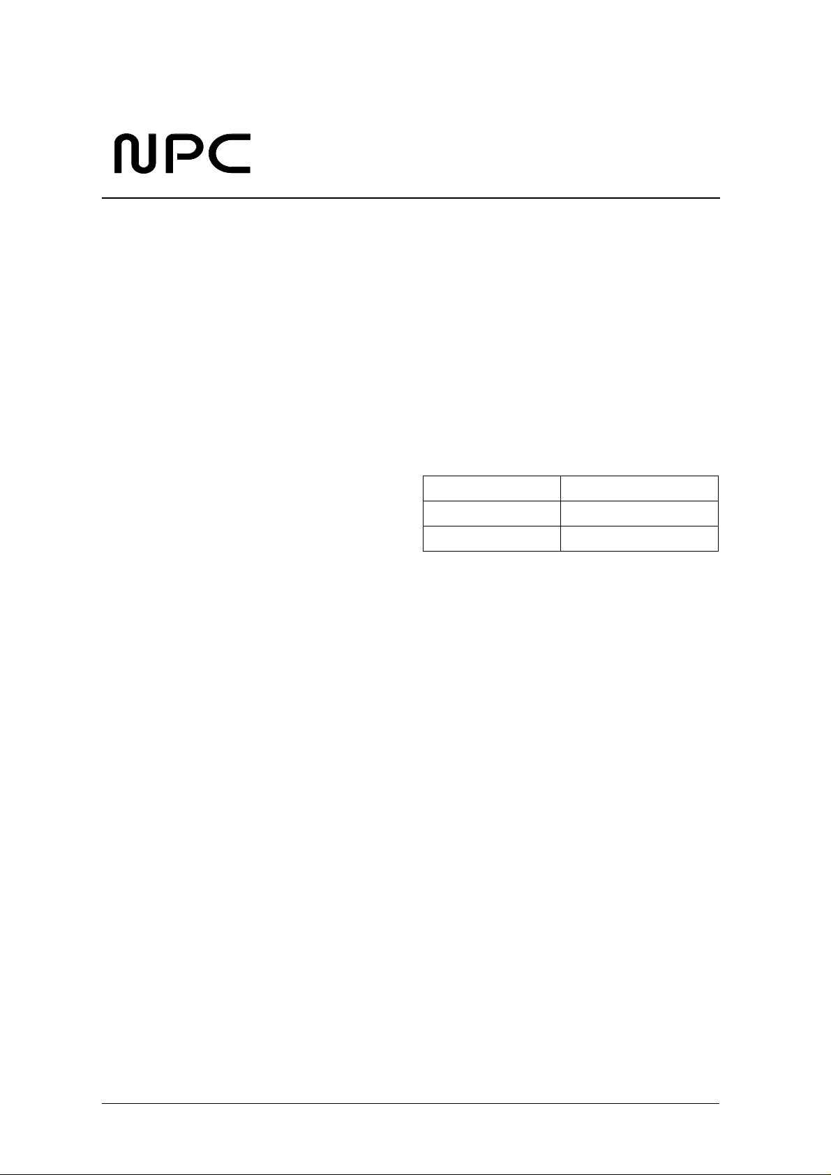
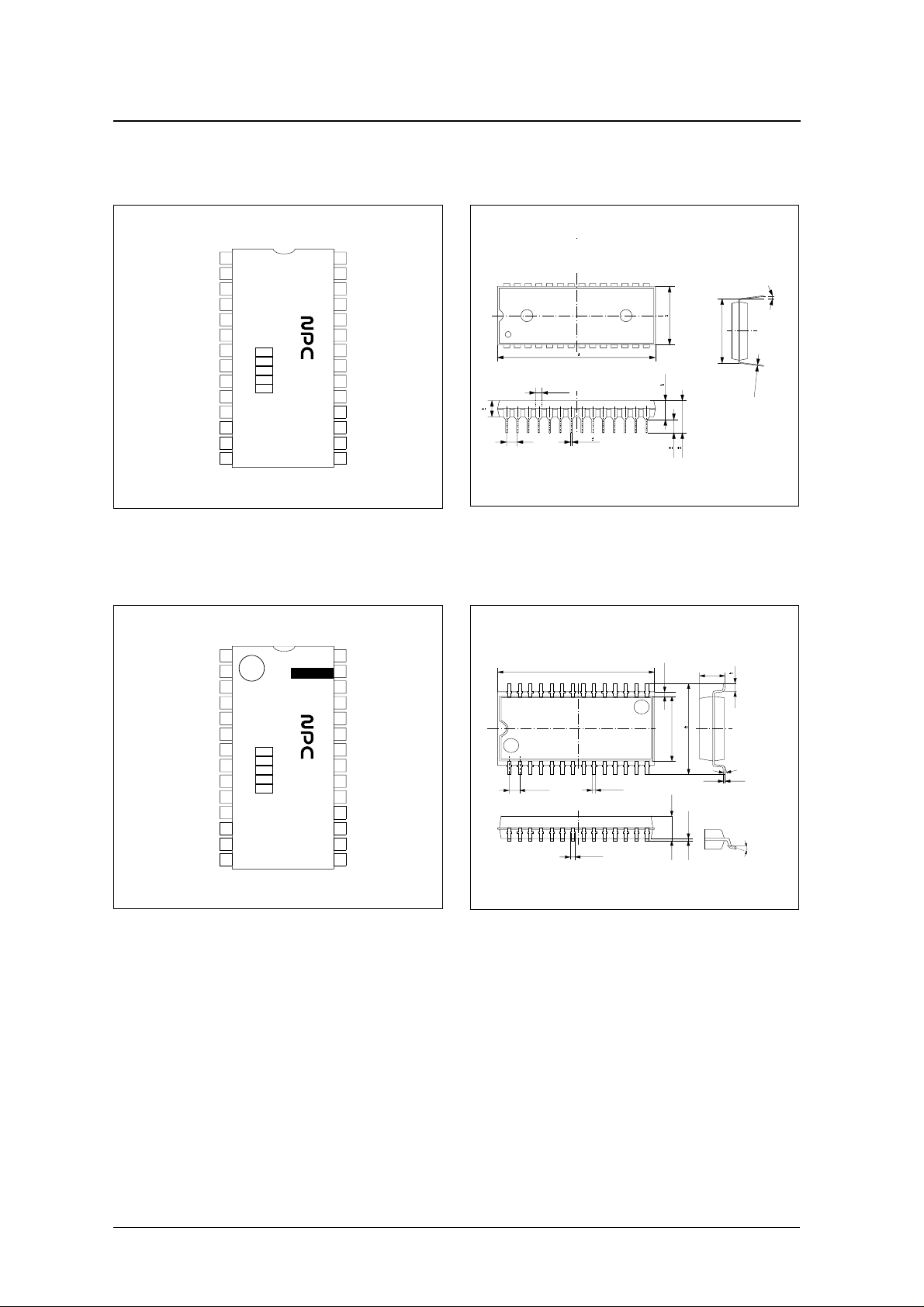
PINOUT
28-pin DIP
(TOP VIEW)
1DI / INF2N
2BCKI
3CKSLN
4INF1N
5IW1N / DIL
6XTI
7XTO
8VSS
9CKO
10IW2N / DIR
11MDT
12MDK
13MLEN
14RSTN 15 MUTE
28 LRCI
27 TMOD2
26 BCKO
SM5843AP1
25 WCKO
24 DOL
23 DOR
22 VDD
21 TMOD1
20 SYNCN
19 OW20N
18 FSEL2
17 FSEL1
16 DEMP
PACKAGE DIMENSIONS
28-pin DIP
3.8 0.1
2.54
28-pin SOP 28-pin SOP
(Unit: mm)
0° to 15°
13.8 0.2
37.3 0.3
+
0.30
1.5
0.05
−
0.45 0.1
4.5 0.3
3.2 0.2
3.2 0.2
7.7 0.5
15.2
0.10
0.05
+
−
0.25
1DI / INF2N
2BCKI
3CKSLN
4INF1N
5IW1N / DIL
6XTI
7XTO
8VSS
9CKO
10IW2N / DIR
11MDT
12MDK
13MLEN
14RSTN 15 MUTE
SM5843AS1
28 LRCI
27 TMOD2
26 BCKO
25 WCKO
24 DOL
23 DOR
22 VDD
21 TMOD1
20 SYNCN
19 OW20N
18 FSEL2
17 FSEL1
16 DEMP
1.27 ± 0.15
18.3 TYP
0.45TYP.
+ 0.10
0.4 − 0.05
0.6MAX.
8.4TYP
3.0MAX.
11.8 0.3
0.10MIN.
3.0MAX
1.0 0.2
0° to 10°
0.15 − 0.05
+ 0.10
0° to 10°
NIPPON PRECISION CIRCUITS—2
Page 3
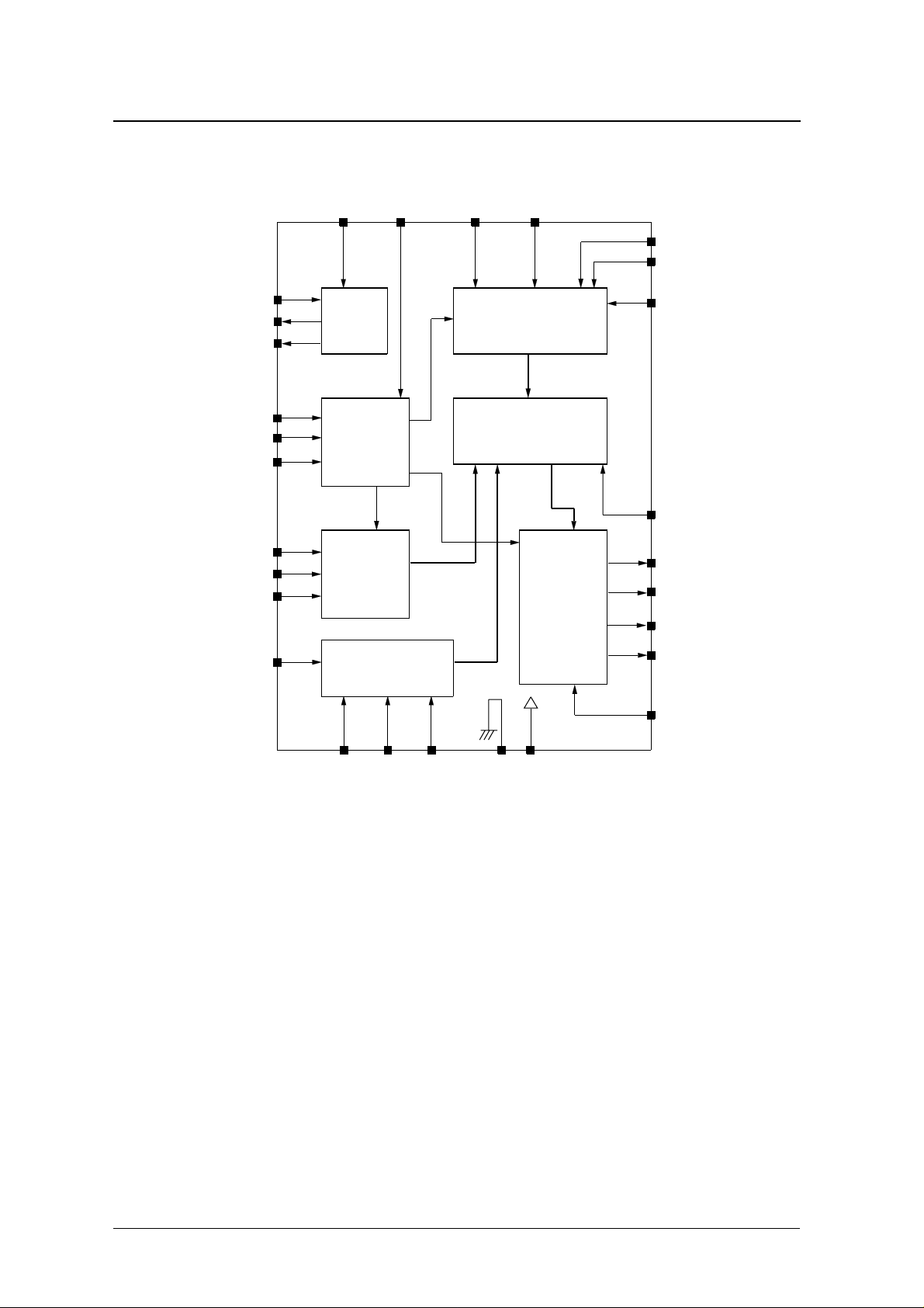
BLOCK DIAGRAM
SM5843A × 1
CKSLN LRCI BCKI DI / INF2N
IW1N / DIL
IW2N / DIR
XTI
XTO
CKO
TOMD2
RSTN
SYNCN
DEMP
FSEL1
FSEL2
MUTE
System
Clock
Timing
Controller
Deemphasis
Controller
Mute/ Attenuation
Controller
Input data Interface
Filter and Attenuation
Arithmetic block
Output date
Interface
INF1N
TMOD1
BCKO
WCKO
DOL
DOR
OW20N
MDT
MCK
VDDMLEN VSS
NIPPON PRECISION CIRCUITS—3
Page 4
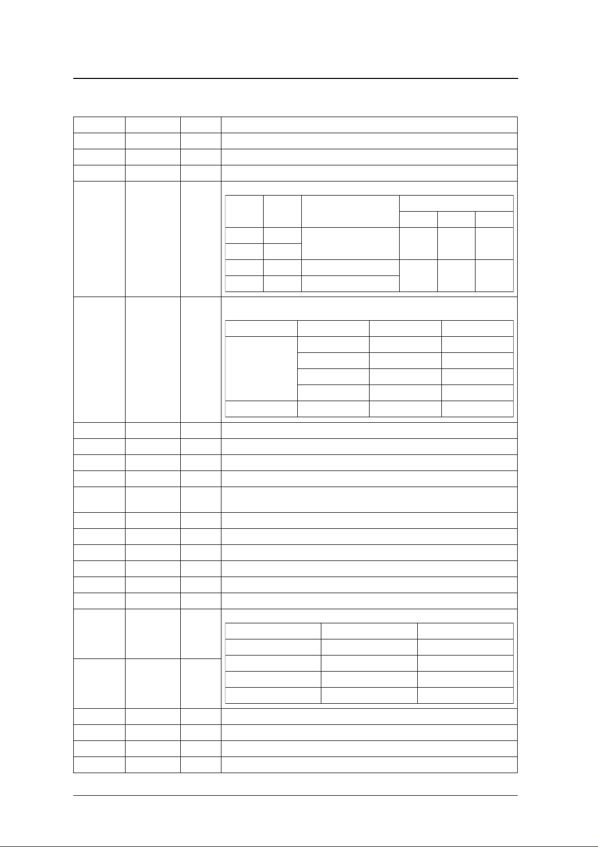
PIN DESCRIPTION
SM5843A × 1
Number Name I/O
1 DI/INF2N Ip Data input when INF1N is LOW, and input format select pin when INF1N is HIGH.
2 BCKI Ip Input bit clock
3 CKSLN Ip Oscillator and system clock select input. 384fs when HIGH, and 256fs when LOW.
4 INF1N Ip
5 IW1N/DIL Ip
1
Input format select pin. INF1N and INF2N select the pin functions below.
INF1N DI/INF2N Input format
LOW LOW
LR alternating, trailing data DI IW1N IW2N
LOW HIGH
HIGH LOW LR alternating, leading data
HIGH HIGH LR simultaneous, leading data
Input bit length select pin when INF1N is LOW, and left-channel data input when INF1N is HIGH.
IW1N and IW2N select the input data length.
INF1N IW2N/DIL IW1N/DIR Input bit length
LOW
HIGH ××20 bits
Description
Pin function selection
DI/INF2N IW1N/DIL IW2N/DIR
INF2N DIL DIR
LOW LOW 20 bits
LOW HIGH 20 bits
HIGH LOW 18 bits
HIGH HIGH 16 bits
6 XTI I Oscillator input connection
7 XTO O Oscillator output connection
8 VSS – Ground
9 CKO O Oscillator output clock. Same frequency as XTI.
10 IW2N/DIR Ip
11 MDT Ip Attenuator serial data input
12 MCK Ip Attenuator bit clock input
13 MLEN Ip Attenuator latch enable input
14 RSTN Ip System reset. Reset operation when LOW, and normal operation when HIGH.
15 MUTE Ip Mute control signal. Muting when HIGH, and normal operation when LOW.
16 DEMP Ip Deemphasis control signal. OFF when LOW, and ON when HIGH.
17 FSEL1 Ip
18 FSEL2 Ip
19 OW20N Ip Output bit length select pin. 20-bit output when LOW, and 18-bit output when HIGH.
20 SYNCN Ip Sync mode select pin. Normal sync mode when LOW, and jitter-free mode when HIGH.
21 TMOD1 Ip Dither processing control. ON when LOW, and OFF when HIGH.
22 VDD – 5 V supply
Input bit length select pin when INF2N is LOW, and right-channel data input when INF2N is HIGH.
IW1N and IW2N select the input data length as shown in the table for pin 5.
Deemphasis filter select inputs
FSEL1 FSEL2 Sampling frequency (fs)
LOW LOW 44.1 kHz
LOW HIGH 48 kHz
HIGH LOW Test mode
HIGH HIGH 32 kHz
NIPPON PRECISION CIRCUITS—4
Page 5

SM5843A × 1
Number Name I/O
23 DOR O Right-channel data output
24 DOL O Left-channel data output
25 WCKO O Output word clock
26 BCKO O Output bit clock
27 TMOD2 Ip
28 LRCI Ip Input data sample rate (fs) clock
1. I = input, Ip = Input with pull-up resistor, O = output
1
Filter characteristic select pin. Sharp roll-off (response 1) when HIGH, and slow roll-off (response 2)
when LOW.
Description
NIPPON PRECISION CIRCUITS—5
Page 6
SM5843A × 1
SPECIFICATIONS
Absolute Maximum Ratings
V
= 0 V
SS
Parameter Symbol Rating Unit
Supply voltage range V
Input voltage range V
Storage temperature range T
Power dissipation P
Soldering temperature T
Soldering time t
−
−
+
−
°
°
−
° C
−
° C
DD
IN
stg
0.3 to 7.0 V
0.3 to V
0.3 V
DD
40 to 125
C
550 (DIP)
D
sld
sld
390 (SOP)
255
10 s
mW
C
Recommended Operating Conditions
fs = 384fs (CKSLN = HIGH): V
Parameter Symbol Rating Unit
Supply voltage range V
Operating temperature range T
fs = 256fs (CKSLN = LOW): V
Parameter Symbol Rating Unit
Supply voltage range V
Operating temperature range T
SS
SS
= 0 V
= 0 V
DD
opr
DD
opr
4.5 to 5.5 V
20 to 80
4.75 to 5.25 V
20 to 70
DC Electrical Characteristics
V
= 4.5 to 5.5 V, V
DD
Parameter Symbol Condition
Current consumption I
XTI HIGH-level input voltage V
XTI LOW-level input voltage V
XTI AC-coupled input voltage V
HIGH-level input voltage
LOW-level input voltage
HIGH-level output voltage
LOW-level output voltage
XTI HIGH-level input current I
XTI LOW-level input current I
LOW-level input current
Input leakage current
1. f
= 256fs = 14.2 MHz (CKSLN = LOW), no output load
SYS
2. Pins DI/INF2N, BCKI, CKSLN, INF1N, IW1N/DIL, IW2N/DIR, MDT, MCK, MLEN, RSTN, MUTE, DEMP, FSEL1, FSEL2, OW20N, SYNCN, LRCI,
TMOD1, TMOD2
3. Pins CKO, DOL, DOR, BCKO, WCKO
= 0 V, T
SS
= − 20 to 80 ° C
a
Rating
Unit
min typ max
DD
IH1
IL1
INAC
2
2
3
3
2
2
V
IH2
V
IL2
V
OH
V
OL
IH
IL1
I
IL2
I
LH
V
DD
I
OH
I
OL
V
IN
V
IN
V
IN
V
IN
1
= 5.0 V
= − 0.4 mA 2.5 – – V
= 1.6 mA – – 0.4 V
= V
DD
= 0 V – 10 20 µA
= 0 V – 10 20 µA
= V
DD
–5065mA
0.7V
DD
– – 0.3V
0.3V
DD
––V
DD
––V
V
p-p
2.4 – – V
– – 0.5 V
–1020µA
– – 1.0 µA
NIPPON PRECISION CIRCUITS—6
Page 7
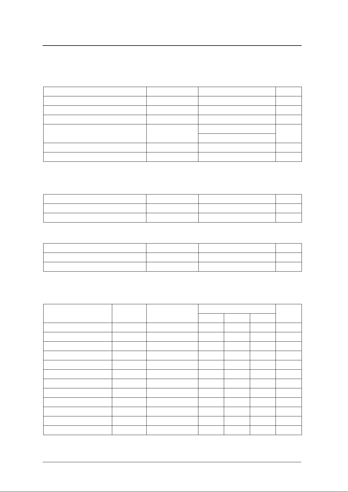
AC Electrical Characteristics
Input Clock (XTI)
Crystal oscillator
SM5843A × 1
fs = 384fs (CKSLN = HIGH): V
Parameter Symbol
Oscillator frequency f
fs = 256fs (CKSLN = LOW): V
Parameter Symbol
Oscillator frequency f
= 4.5 to 5.5 V, V
DD
= 4.75 to 5.25 V, V
DD
External clock input
fs = 384fs (CKSLN = HIGH): V
Parameter Symbol
Clock HIGH-level pulsewidth t
Clock LOW-level pulsewidth t
Clock pulse cycle time t
= 4.5 to 5.5 V, V
DD
OSC
OSC
CWH
CWL
XI
= 0 V, T
SS
= 0 V, T
SS
= 0 V, T
SS
= − 20 to 80 ° C
a
Rating
min typ max
2.0 – 21.2 MHz
= − 20 to 70 ° C
a
Rating
min typ max
1.0 – 14.2 MHz
= −20 to 80 °C
a
Rating
min typ max
20 – 250 ns
20 – 250 ns
47 – 500 ns
Unit
Unit
Unit
fs = 256fs (CKSLN = LOW): VDD = 4.75 to 5.25 V, VSS = 0 V, Ta = −20 to 70 °C
Parameter Symbol
Clock HIGH-level pulsewidth t
Clock LOW-level pulsewidth t
Clock pulse cycle time t
XTI
tCWH
CWH
CWL
XI
min typ max
30 – 500 ns
30 – 500 ns
70 – 1000 ns
tCWL
Rating
VlH1
0.5VDD
VlL1
tXI
Unit
NIPPON PRECISION CIRCUITS—7
Page 8
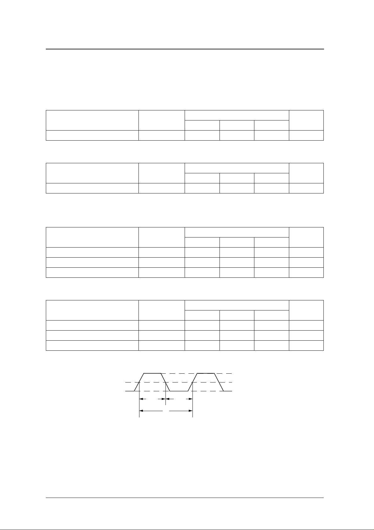
Serial input timing (BCKI, DI, DIL, DIR, LRCI)
VDD = 4.5 to 5.5 V, VSS = 0 V, Ta = −20 to 80 °C
SM5843A×1
Parameter Symbol
BCKI HIGH-level pulsewidth t
BCKI LOW-level pulsewidth t
BCKI pulse cycle t
DIN setup time t
DIN hold time t
Last BCKI rising edge to LRCI edge t
LRCI edge to first BCKI rising edge t
BCKI
DI
DIL
DIR
BCWH
BCWL
BCY
DS
DH
BL
LB
tDS
Rating
min typ max
50 – – ns
50 – – ns
100 – – ns
50 – – ns
50 – – ns
50 – – ns
50 – – ns
Unit
tBCY
tBCWH
tBCWL
1.5V
tDH
1.5V
LRCI
Reset timing (RSTN)
VDD = 4.5 to 5.5 V, VSS = 0 V, Ta = −20 to 80 °C
Parameter Symbol Condition
RST
LOW-level reset pulsewidth t
RST
At power-ON 1 – – µs
At all other times 50 – – ns
tBL
Rating
min typ max
tLB
1.5V
Unit
NIPPON PRECISION CIRCUITS—8
Page 9

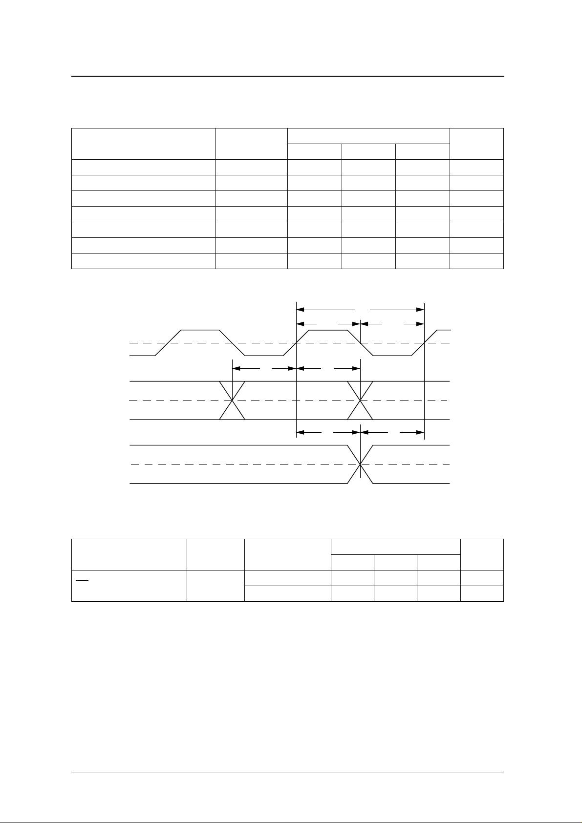
Attenuator timing (MDT, MCK, MLEN)
VDD = 4.5 to 5.5 V, VSS = 0 V, Ta = −20 to 80 °C
SM5843A×1
Parameter Symbol
MDT setup time t
MDT hold time t
MLEN setup time t
MLEN hold time t
MLEN LOW-level pulsewidth t
MLEN HIGH-level pulsewidth t
MLEN pulse cycle time t
1. t
= 1/384fs when CKSLN is HIGH, and 1/256fs when CKSLN is LOW.
SYS
MDT
tMDS tMDH
MCK
MDS
MDH
MCS
MCH
MEWL
MEWH
MLEY
Rating
min typ max
20 – – ns
20 – – ns
40 – – ns
20 – – ns
20 – – ns
20 – – ns
6––t
Unit
SYS
1
1.5V
1.5V
MLEN
tMCS tMCH
tMEWL
tMLEY
1.5V
tMEWH
NIPPON PRECISION CIRCUITS—9
Page 10

SM5843A×1
Output timing
VDD = 4.5 to 5.5 V, VSS = 0 V, Ta = −20 to 80 °C, CL = 15 pF
Parameter Symbol Condition
XTI to XTO delay t
XTI to CKO delay t
XTI to BCKO delay (CKSLN = HIGH)
XTI to BCKO delay (CKSLN = LOW)
BCKO to DOL, DOR, WCKO delay
CKO TODOL, DOR, WCKO delay
XTO TODOL, DOR, WCKO delay
XTI
(CKSLN = H)
XTO
CKO
t
sbH
t
sbL
t
sbH
t
sbL
t
bdH
t
bdL
t
cdH
t
cdL
t
xdH
t
xdL
Rating
Unit
min typ max
XTI fall to XTO rise 3 – 15 ns
XTI fall to CKO fall 10 – 35 ns
XTI fall to BCKO rise 20 – 60
ns
XTI fall to BCKO fall 20 – 60
XTI fall to BCKO rise 20 – 60
ns
XTI fall to BCKO fall 20 – 60
BCKO fall to output rise −5–10
ns
BCKO fall to output fall −5–10
CKO fall to output rise 5 – 25
ns
CKO fall to output fall 5 – 25
XTO rise to output rise 15 – 50
ns
XTO rise to output fall 15–50
Tsys Tsys
0.5VDD
tCKO
CKO
(CKSLN = H)
XTI
(CKSLN = L)
CKO
(CKSLN = L)
BCKO
DOL
DOR
WCKO
Tsys
tsbH
XTO rising edge
XTO rising edge
tsbL
tCKO
tcdL
tbdL
tbdH
tcdH
txdH
txdL
1.5V
0.5VDD
1.5V
1.5V
1.5V
1.5V
NIPPON PRECISION CIRCUITS—10
Page 11

SM5843A×1
Filter Characteristics
8-times interpolation filter (sharp roll-off: response 1)
Parameter Condition Rating @ 256fs
Passband 0 to 0.4535fs
Stopband 0.5465fs to 7.4535fs
Passband ripple ≤ ±0.00005 dB
Stopband attenuation ≥ 110 dB
Group delay
1
1. The digital filter arithmetic computation time from when the completion of data input at rate fs to the start of data output at rate 8fs.
8fs filter response with deemphasis OFF
0
20
40
(dB)
60
SYNCN = LOW 44.625/fs
SYNCN = HIGH 44.25/fs to 45.0/fs
80
Attenuation
100
120
140
0.0 1.0 2.0 3.0 4.0 5.0 6.0 7.0 8.0
Frequency
8fs filter band transition response with deemphasis OFF
0
20
40
(dB)
60
80
Attenuation
100
120
140
0.440 0.465 0.490 0.515 0.540 0.565 0.6150.590 0.640
Frequency
8fs filter passband response with deemphasis OFF
(×fs)
(×fs)
-0.0001
-0.00005
(dB)
0.00000
0.00005
Attenuation
0.0001
0.000 0.125 0.250 0.375 0.500
Frequency
(×fs)
NIPPON PRECISION CIRCUITS—11
Page 12

SM5843A×1
8-times interpolation filter (slow roll-off: response 2)
Parameter Condition Rating @ 256fs
Passband < 3 dB attenuation 0 to 0.455fs
Stopband > 77 dB attenuation 0.745fs to 7.255fs
Passband ripple 0 to 0.235fs ≤ ±0.00003 dB
Stopband attenuation ≥ 77 dB
Group delay
1
1. The digital filter arithmetic computation time from when the completion of data input at rate fs to the start of data output at rate 8fs.
8fs filter response with deemphasis OFF
0
20
40
(dB)
60
SYNCN = LOW 25.625/fs
SYNCN = HIGH 25.25/fs to 26.0/fs
80
Attenuation
100
120
140
0.0 1.0 2.0 3.0 4.0 5.0 6.0 7.0 8.0
Frequency
8fs filter band transition response with deemphasis OFF
0
20
40
(dB)
60
80
Attenuation
100
120
140
0.00 0.125 0.25 0.375 0.50 0.625 0.75 0.825 1.00
Frequency
8fs filter passband response with deemphasis OFF
(×fs)
(×fs)
-2.0
0.0
(dB)
2.0
4.0
Attenuation
6.0
0.000 0.125
0.250 0.375
Frequency
(×fs)
0.500
NIPPON PRECISION CIRCUITS—12
Page 13

SM5843A×1
8fs filter passband response [amplitude gain enlarged]
-0.0001
-0.00005
(dB)
0.00000
0.00005
Attenuation
0.0001
0.000 0.125 0.250 0.375 0.500
Frequency
Deemphasis filter
(×fs)
Parameter
32 kHz 44.1 kHz 48 kHz
Passband bandwidth (kHz) 0 to 14.5 0 to 20.0 0 to 21.7
Attenuation ≤ ±0.001 dB
Deviation from ideal characteristic
Phase, θ 0 to 1.5°
Sampling frequency (fs)
Passband response with deemphasis ON (logarithmic frequency axis)
0
2
4
6
8
Attenuation (dB)
32kHz
44.1kHz
48kHz
Attenuation
32k A44.1k A48kHz
Phase
0
-20
-40
Phase θ ( ° )
-60
10
10 20 50 100 200 500 1k 2k 5k 10k 20k
Frequency (Hz)
Passband response with deemphasis ON (linear frequency axis)
0
2
32kHz
4
6
Attenuation (dB)
8
Attenuation
32k A44.1k A48kHz
10
0 4k 8k 12k 16k 22k20k 24k
Frequency (Hz)
Phase
0
-20
44.1kHz
48kHz
-40
Phase θ ( ° )
-60
NIPPON PRECISION CIRCUITS—13
Page 14

SM5843A×1
FUNCTIONAL DESCRIPTION
The basic arithmetic block is shown in figure 1, and
the function of each block is described in the following sections.
Input
2 - times oversampling
153 - tap (response 1 )or
25 - tap (response 2 )
FIR
2 - times oversampling
29 - tap FIR
4fs
Deemphasis OFF
fs
2fs
Deemphasis IIR
filter
Deemphasis ON
Mute function
2 - times oversampling
17 - tap FIR
Output
Figure 1. Arithmetic block diagram
8-times Oversampling (Interpolation)
The interpolation arithmetic block is comprised of 3
cascaded, 2-times FIR interpolation filters, as shown
in figure 1.
The input signal is sampled at rate fs, and then 8times oversampling data is output. Sampling noise in
the 0.5465fs to 7.4535fs stopband for the sharp rolloff (response 1) characteristic, 0.745fs to 7.255fs for
the slow roll-off (response 2) characteristic, is
removed by the interpolation filter.
4fs
4fs
8fs
Digital Deemphasis
The digital deemphasis filter has the same construction as analog filters. It is implemented as an IIR filter to faithfully reproduce the gain and phase
characteristics of standard analog deemphasis filters.
The three sets of filter coefficients for the three fs =
32.0/44.1/48.0 kHz sampling frequencies are
selected by FSEL1 and FSEL2 when the sampling
frequency is specified, as shown in the following
table. Deemphasis is ON when DEMP is HIGH, and
OFF when DEMP is LOW.
FSEL1 FSEL2 Sampling frequency (fs)
LOW LOW 44.1 kHz
LOW HIGH 48 kHz
HIGH LOW Test mode
HIGH HIGH 32 kHz
Note that test mode is not available for operation.
NIPPON PRECISION CIRCUITS—14
Page 15

Soft Muting
SM5843A×1
The muting function controls the muting of both left
and right channels simultaneously. Muting is ON
when MUTE is HIGH, muting is OFF when MUTE
is LOW.
MUTE
0dB
(Gain)
−∞
LH L
512 / fs
Figure 2. Mute timing
When RSTN goes LOW, the DOL and DOR outputs
go LOW, immediately muting the output signal.
Digital Attenuator (MDT, MCK, MLEN)
The attenuation function is controlled by MDT,
MCK and MLEN. MDT data, in 11-bit serial MSB
first format, is shifted into an internal shift register
on the rising edge of the serial data clock MCK. The
When MUTE goes HIGH, the attenuation changes
smoothly from 0 to −∞ dB in 512/fs, or approximately 11.6 ms when fs = 44.1 kHz. When MUTE
goes LOW, muting is released and the attenuation
changes smoothly from −∞ to 0 dB, again taking
approximately 11.6 ms.
512 / fs
Muting is released and timing is synchronized immediately after RSTN goes HIGH.
contents of the shift register are transferred to the
internal processing circuits on the rising edge of the
MLEN gate pulse. The attenuation data format is
shown in figure 3.
B1 B2 B3 B4 B5 B6 B7 B8 B9 B10 B11
MDT
MCK
MLEN
a0 a1 a2 a3 a4 a5 a6 a7 a8 a9 a10
MSB LSB
Figure 3. Attenuation data format
The attenuation register data DATT can take on any
value between 0 and 1024 (400H). The attenuation is
given by the following equation for both left and
right channels simultaneously.
Attenuation = 20 × log10(DATT/1024) [dB]
Thus, the attenuation level is −∞ when DATT is 0,
and attenuation is 0 dB when DATT is 1024. DATT
is set to 1024 (400H) after system reset initialization.
The attenuation data and attenuation level for sample
DATT values are shown in the following table.
Attenuation data DATT Attenuation level (dB)
000
001
3FF
400
H
H
to
H
H
−∞
−60.206
to
−0.0085
0
NIPPON PRECISION CIRCUITS—15
Page 16

SM5843A×1
Attenuation operation
When an attenuation value DATT is set, the attenuation changes smoothly from the current attenuation
level to the new level. The new attenuation data is
stored in the attenuation register while the current
attenuation data is stored in a temporary register . The
attenuation then changes smoothly by ramping
between the two register values, updating the temporary register with each step. If a new attenuation
value for DATT is set before the previous target
attenuation level is reached, the attenuation then
ramps toward the new attenuation level.
When MUTE is HIGH, the attenuation level is −∞.
When MUTE goes LOW (muting OFF), the attenuation level returns to that of the original value of
DATT.
Setting1
DATT1
(Gain)
−∞
MUTE
DATT2
Setting2
LH L
Figure 4. Attenuation and mute timing
System Clock (XTI, XTO, CKO, CKSLN)
Two system clock frequencies, 384fs and 256fs, can
be used. An external clock source can be input on
XTI, or a crystal oscillator can be constructed by
connecting a crystal between XTI and XTO. The
system clock is also buffered and then output on
CKO. The system clock frequency selection and the
internal clock frequency are shown in the following
table.
Setting4
DATT4
DATT2
DATT3
Setting3
Time
Parameter
XTI input clock frequency (fXI = 1/tXI) 384fs 256fs
CKO clock frequency 384fs 256fs
Internal clock frequency (t
)2 × t
SYS
CKSL
HIGH LOW
t
XI
XI
CKSLN
XTI
XTO
CKO
to timing controller
1 / 2
Internal system clock
(192fs or 256fs)
Figure 5. Clock generator circuit
NIPPON PRECISION CIRCUITS—16
Page 17

SM5843A×1
Audio Data Input (INF1N, INF2N, IW1N,
IW2N, DI, DIL, DIR, BCKI, LRCI)
INF1N DI/INF2N Input format
LOW LOW
LR alternating1, trailing data DI IW1N IW2N
LOW HIGH
HIGH LOW LR alternating, leading data
HIGH HIGH LR simultaneous2, leading data
1. Alternating left-channel and right-channel data input on a single input DI.
2. Simultaneous left-channel and right-channel data input on two inputs, DIL and DIR, respectively.
The input data word length is selected by the state of
IW1N and IW2N when INF1N is LOW. 20-bit is
selected when INF1N is HIGH.
INF1N IW2N/DIL IW1N/DIR Input bit length
LOW LOW 20 bits
LOW HIGH 20 bits
LOW
HIGH LOW 18 bits
HIGH HIGH 16 bits
HIGH ×× 20 bits
The input data format and several input pin functions
are selected by the state of INF1N and INF2N.
exceeds a certain value. There are 2 timing error values at which resynchronization occurs, selected by
the state of SYNCN.
Jitter-free mode (SYNCN = HIGH)
When SYNCN is HIGH, the timing error value is
±3/8 × (LRCI clock period). When the difference
between the input timing and LRCI start edge position do not exceed this value, internal timing is not
resynchronized and all functions continue to operate
normally.
Pin function selection
DI/INF2N IW1N/DIL IW2N/DIR
INF2N DIL DIR
Jitter-free Function (SYNCN)
Sync mode (SYNCN = LOW)
When SYNCN is LOW, the timing error value is ±1
The arithmetic circuit and output control timing is
derived from the system clock, and is therefore independent of the input LRCI and BCKI clocks.
Accordingly, any jitter in the data input clock (LRCI
and BCKI) does not cause jitter in the output.
Generally, the internal timing is synchronized to the
LRCI input timing after a system reset release, when
RSTN goes from LOW to HIGH, on the first LRCI
clock start edge. If the input timing and LRCI start
× (system clock period), which is a much smaller
timing error tolerance than in jitter-free mode. In this
mode, the internal timing is guaranteed to follow the
LRCI clock timing within this tolerance, making this
mode useful for systems constructed from a multiple
number of SM5843A×1 devices.
Note that resynchronization affects the internal operation and can generate a momentary click noise output.
edge timing subsequently drift, the input timing is
automatically resynchronized when the timing error
Audio Data Output (DOL, DOR, BCKO, WCKO, OW20N)
The output data is in serial, simultaneous left and
right-channel, 2s complement, MSB first, BCKO
burst (NPC format) format. The output data word
length is selected by the state of OW20N. 18-bit output is selected when OW20N is HIGH, and 20-bit
output when OW20N is LOW.
8fs serial data is output in sync with the falling edge
of the internal system clock and BCKO clock. The
number of BCKO bit clock pulses per word changes
depending on the output bit length selected (18/20
bits). Consequently, output data is latched into the
internal output register on the falling of the edge of
an output word clock WCKO, which has timing
independent of the number of output bits as specified
in the following table.
Parameter Symbol CKSLN = HIGH CKSLN = LOW
Bit clock rate T
Data word length T
DW
B
1/192fs 1/256fs
24t
SYS
32t
SYS
NIPPON PRECISION CIRCUITS—17
Page 18

System Reset (RSTN)
SM5843A×1
The SM5843A×1 must be reset under the following
conditions.
■ At power-ON.
■ When the LRCI clock and internal operation tim-
ing need to be resynchronized.
■ When switching the CKSLN clock select input.
■ When switching between filter characteristics
using TMOD2.
■ When either or both of the LRCI and XTI clocks
stop or are interrupted.
The system is reset by applying a LOW-level pulse
on RSTN.
The arithmetic and output timing counters are reset
on the first LRCI start edge after reset is released, as
long as the XTI clock has already stabilized. The
LRCI start edge is determined by the state of INF1N
RSTN
LRCI
Internal reset
and INF2N. When INF1N is LOW or when both
INF1N and INF2N are HIGH, the start edge is the
rising edge. When INF1N is HIGH and INF2N is
LOW, the start edge is the falling edge.
When RSTN is LOW, the DOL and DOR outputs are
LOW, muting the output signal to an attenuation
level of −∞.
The power-ON reset pulse can be applied by a
microcontroller or, for systems where XTI and LRCI
are stable at power-ON, by connecting a capacitor of
several hundred pF between RSTN and VSS. For
systems that do not use a microcontroller, the capacitor must be chosen such that the XTI and LRCI
clocks fully stabilize before RSTN goes from LOW
to HIGH.
1 2
WCKO
DOL
DOR
Figure 6. System reset timing and output muting
Filter Characteristic Selection (TMOD2)
There are 2 digital filter frequency response characteristics incorporated into the SM5843A×1, selected
by the state of TMOD2. A sharp roll-off characteristic (response 1) is selected when TMOD2 is HIGH,
and a slow roll-off characteristic (response 2) when
TMOD2 is LOW. The response is modified by
changing the number of taps in the 1st FIR filter
stage, as shown in figure 1.
■ Filter response 1
• 153-tap 1st FIR
• 29-tap 2nd FIR
• 17-tap 3rd FIR
■ Filter response 2
• 25-tap 1st FIR
• 29-tap 2nd FIR
• 17-tap 3rd FIR
Note that the device should be reset when changing
TMOD2 during normal operation.
Dither Rounding-off Processing
(TMOD1)
Dither rounding-off processing of output data is ON
when TMOD1 is LOW. Dither is OFF and normal
processing mode is selected when TMOD1 is HIGH.
NIPPON PRECISION CIRCUITS—18
Page 19

SM5843A×1
TIMING DIAGRAMS
Input Timing Examples (DIN, BCKI, LRCI)
Lch DATA Rch DATA
1 2 14 15 16 1 2 14 15 16
Lch DATA
19 20
BCKI
LRCI
DIL
DIR
(MSB)
DI
Figure 7. LR alternating, trailing data, 16-bit input
(MSB) (LSB)
123
1 / fs
(LSB) (MSB) (LSB)
1 / fs
Rch DATA
(MSB) (LSB)
123
19 20
1
DIL
DIR
BCKI
LRCI
BCKI
LRCI
Data after lsb (bit 20) is ignored. After bit 20, BCKI clock input is not needed.
Figure 8. LR alternating, leading data, 20-bit input
1 / fs
(MSB)
123 1
(MSB)
12314
Data after lsb (bit20) is ignored. After bit 20, BCKI clock input is not needed.
Lch DATA
456
Rch DATA
5
6
(LSB)
19 2018
(LSB)
19 2018
Figure 9. LR simultaneous, leading data, 20-bit input
NIPPON PRECISION CIRCUITS—19
Page 20

SM5843A×1
Output Timing Examples (DOL, DOR, BCKO, WCKO)
24TB(TDW)
System
Clock
DOL
DOR
BCKO
WCKO
123
1234 18 1917 20 1234
T
B TB
4 18 1917 20 1234
12TB
The number of output bits is determined by the output bit length selected.
Figure 10. 18/20-bit output (CKSL = HIGH)
32TB(TDW)
System
Clock
DOL
DOR
BCKO
WCKO
The number of output bits is determined by the output bit length selected.
T
B TB
123
123
16TB
(*)
(*)
12TB
18 1917 201615
18 1917 201615
(*)
(*)
16TB
12
12
Figure 11. 18/20-bit output (CKSL = LOW)
NIPPON PRECISION CIRCUITS—20
Page 21

Data Input to Output Delay Timing
SM5843A×1
This is the digital filter arithmetic computation time
from the completion of data input at rate fs (t
Filter response CKSLN SYNCN Mode t
LOW (256fs)
Filter response 1
HIGH (384fs)
LOW (256fs)
Filter response 2
HIGH (384fs)
INPUT
on the rising edge of LRCI to the start of data output
)
at rate 8fs (t
LOW After reset + sync mode 44.625/fs
HIGH Jitter-free mode 44.25/fs − 45.0/fs
LOW After reset + sync mode 44.75/fs
HIGH Jitter-free mode 44.375/fs − 45.125/fs
LOW After reset + sync mode 25.625/fs
HIGH Jitter-free mode 25.25/fs − 26.0/fs
LOW After reset + sync mode 25.75/fs
HIGH Jitter-free mode 25.375/fs − 26.125/fs
OUTPUT
) on the falling edge of WCKO.
1/fs
LRCI
Serial data Input
44/fs(Filter Response 1)
25/fs(Filter Response 2)
tINPUT
WCKO
(256fs)
OUTPUT
− t
INPUT
WCKO
tOUTPUT
Serial data output
(384fs)
tOUTPUT
Figure 12. Delay timing (SYNCN = LOW)
44.625/fs (Filter Response 1)
tINPUT
(Filter Response 2)
25.625/fs
tINPUT
tOUTPUT
Figure 13. Delay timing (SYNCN = CKSLN = LOW)
Serial data output
tOUTPUT
NIPPON PRECISION CIRCUITS—21
Page 22

APPLICATION CIRCUITS
Input Interface Circuits
CD decoder (CXD2500Q) connection
SM5843A×1
SONY
CD DECODER
CXD2500Q
PSSL
C16M
LRCK
EMPH
DA16
DA15
16.9344MHz
44.1kHz
2.1168MHz
Digital audio interface receiver (YM3623B) connection
384fs
(16.9344MHz)
øA
fs(44.1kHz)
YAMAHA
DIR
YM3623B
S1 S2
L / R
DO
BCO
DEF
XTI
LRCI
DI
BCKI
DEMP
IW1N
IW2N
INF1N
XTI
LRCI
DI
BCKI
DEMP
IW1N
IW2N
INF1N
CKSLN
SM5843
MUTE
FSEL1
FSEL2
CKSLN
SM5843
MUTE
FSEL1
FSEL2
MUTE
MUTE
NIPPON PRECISION CIRCUITS—22
Page 23

SM5843A×1
Output Interface Circuits
20-bit input Σ∆ DAC (SM5864AP) connection 1
to SIGNAL
PROCESSOR
(CD DECODER)
384fs
CKSLN
CKO
SM5843
(20bitOUT)
OW20N
XTI
BCKO
WCKO
DOL
DOR
384fs
8fs
XDIVN
CKO
BCKI
WCKI
DINL
DINR
COMPN
X3SL
20-bit input Σ∆ DAC (SM5864AP) connection 2
L/R-channel independent complementary PWM output
to SIGNAL
PROCESSOR
(CD DECODER)
384fs
CKSLN
CKO
SM5843
(20bitOUT)
OW20N
XTI
BCKO
WCKO
DOL
DOR
384fs
8fs
XDIVN
CKO
BCKI
WCKI
DINL
DINR
X3SL
COMPN
X'tal
384fs
NPC
Σ∆DAC
SM5864
(ΣDECO)
NPC
Σ∆DAC
SM5864
(ΣDECO)
XTI
74HCU04
XTI
LOA
LOBN
ROA
ROBN
LOA
LOBN
ROA
ROBN
Analog
LPF
Analog
LPF
Analog
LPF
LchOUT
RchOUT
LchOUT
X'tal
384fs
74HCU04
XDIVN
BCKI
WCKI
DINL
DINR
X3SL
COMPN
XTI
NPC
Σ∆DAC
SM5864
(ΣDECO)
LOA
LOBN
ROA
ROBN
Analog
LPF
NIPPON PRECISION CIRCUITS—23
RchOUT
Page 24

SM5843A1
NIPPON PRECISION CIRCUITS INC. reserves the right to make changes to the products described in this data sheet in order to
improve the design or performance and to supply the best possible products. Nippon Precision Circuits Inc. assumes no responsibility for
the use of any circuits shown in this data sheet, conveys no license under any patent or other rights, and makes no claim that the circuits
are free from patent infringement. Applications for any devices shown in this data sheet are for illustration only and Nippon Precision
Circuits Inc. makes no claim or warr anty that such applications will be suitab le for the use specified without further testing or modification.
The products described in this data sheet are not intended to use for the apparatus which influence human lives due to the failure or
malfunction of the products. Customers are requested to comply with applicable laws and regulations in effect now and hereinafter,
including compliance with export controls on the distribution or dissemination of the products. Customers shall not expor t, directly or
indirectly, any products without first obtaining required licenses and approvals from appropriate government agencies.
NIPPON PRECISION CIRCUITS INC.
4-3, Fukuzumi 2-chome
Koto-ku, Tokyo 135-8430, Japan
NIPPON PRECISION CIRCUITS INC.
Telephone: 03-3642-6661
Facsimile: 03-3642-6698
NC9626AE 1997.03
NIPPON PRECISION CIRCUITS—24
 Loading...