

Page 1
SM5838AS
NIPPON PRECISION CIRCUITS INC.
OVERVIEW
The SM5838AS is a 5120 × 8-bit synchronous FIFO
(first in, first out) high-speed line buffer. Internally, it
employs static CMOS circuits which mean that it
effectively has limitless data hold times. It can operate at speeds up to 33.3 MHz (normal-voltage specification).
The SM5838AS can be used to easily realize a 1-line
delay in high-speed facsimile machines and digital
copiers.
FEATURES
■
5120 × 8-bit structure
■
Variable-length delay (21 to 5120 bits)
■
33.3 MHz high-speed operation (normal-voltage
specification)
■
All input/outputs TTL compatible
■
Independent read enable and output enable pins,
allowing read address pointer increment in output
data hold and output high-impedance states
■
Supply voltage
• 4.5 to 5.5 V (normal-voltage specification)
• 3.0 to 4.5 V (low-voltage specification)
■
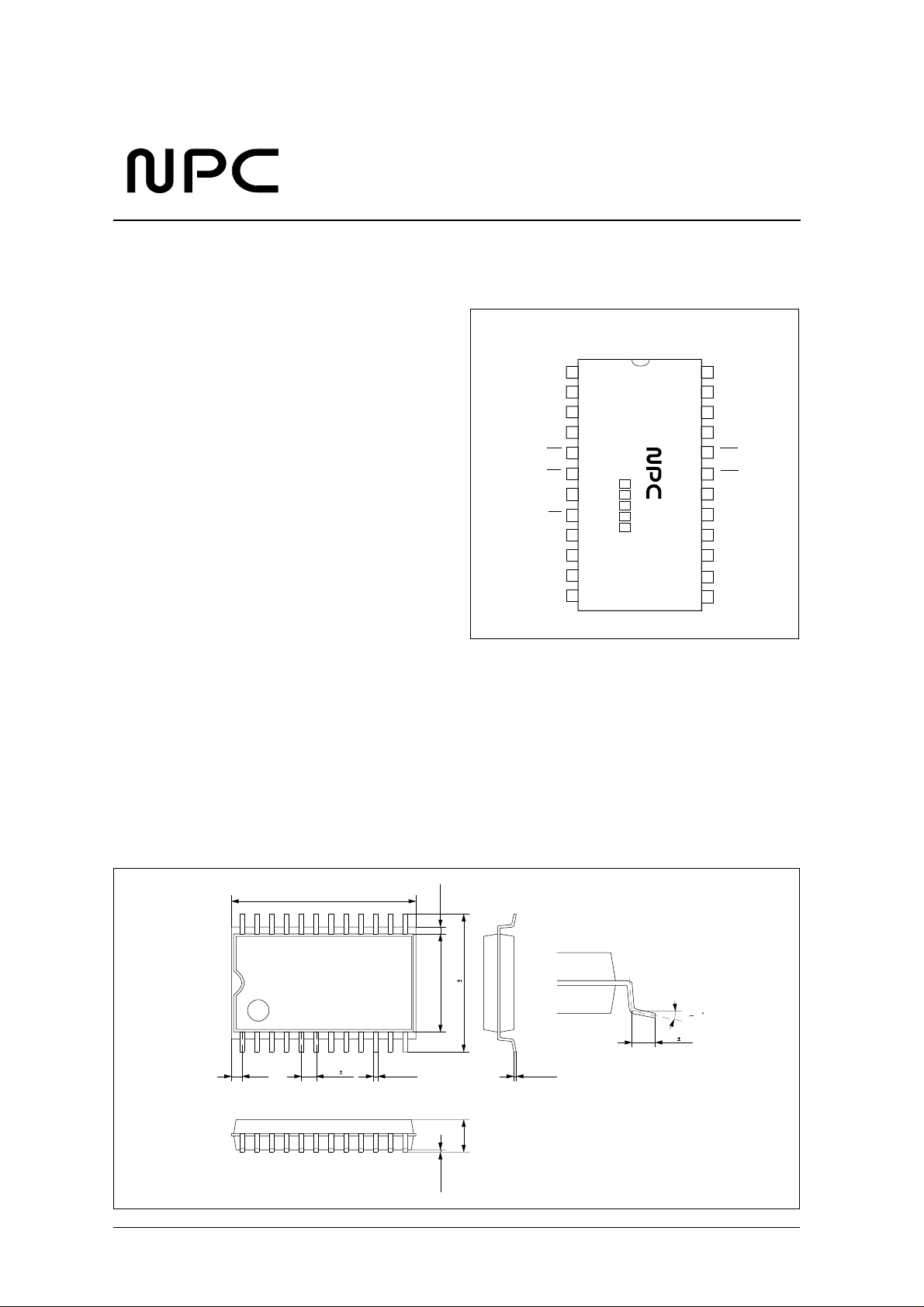
24-pin SOP package
■
Molybdenum-gate CMOS process
■
A3-paper 1-line (16 dots/mm) compatible
5120 × 8-bit Synchronous FIFO
PINOUT
(TOP VIEW)
DOUT0
DOUT1
DOUT2
DOUT3
OE
RR
VSS
RE
DOUT4
DOUT5
DOUT6
DOUT7
1
2
3
4
5
6
718
8
9
10
11
12
SM5838AS
24
DIN0
23
DIN1
DIN2
22
21
DIN3
20
WE
19
RW
VDD
CLK
17
16
DIN4
DIN5
15
14
DIN6
DIN7
13
PACKAGE DIMENSIONS
24-pin SOP (Unit: mm)
15.8TYP
0.915
1.27 0.1
0.6MAX
8.4TYP
11.8 0.3
010
1.0 0.2
+ 0.10
0.4
- 0.05
2.5MAX
0.10MIN
0.17
+ 0.08
- 0.07
NIPPON PRECISION CIRCUITS—1
Page 2
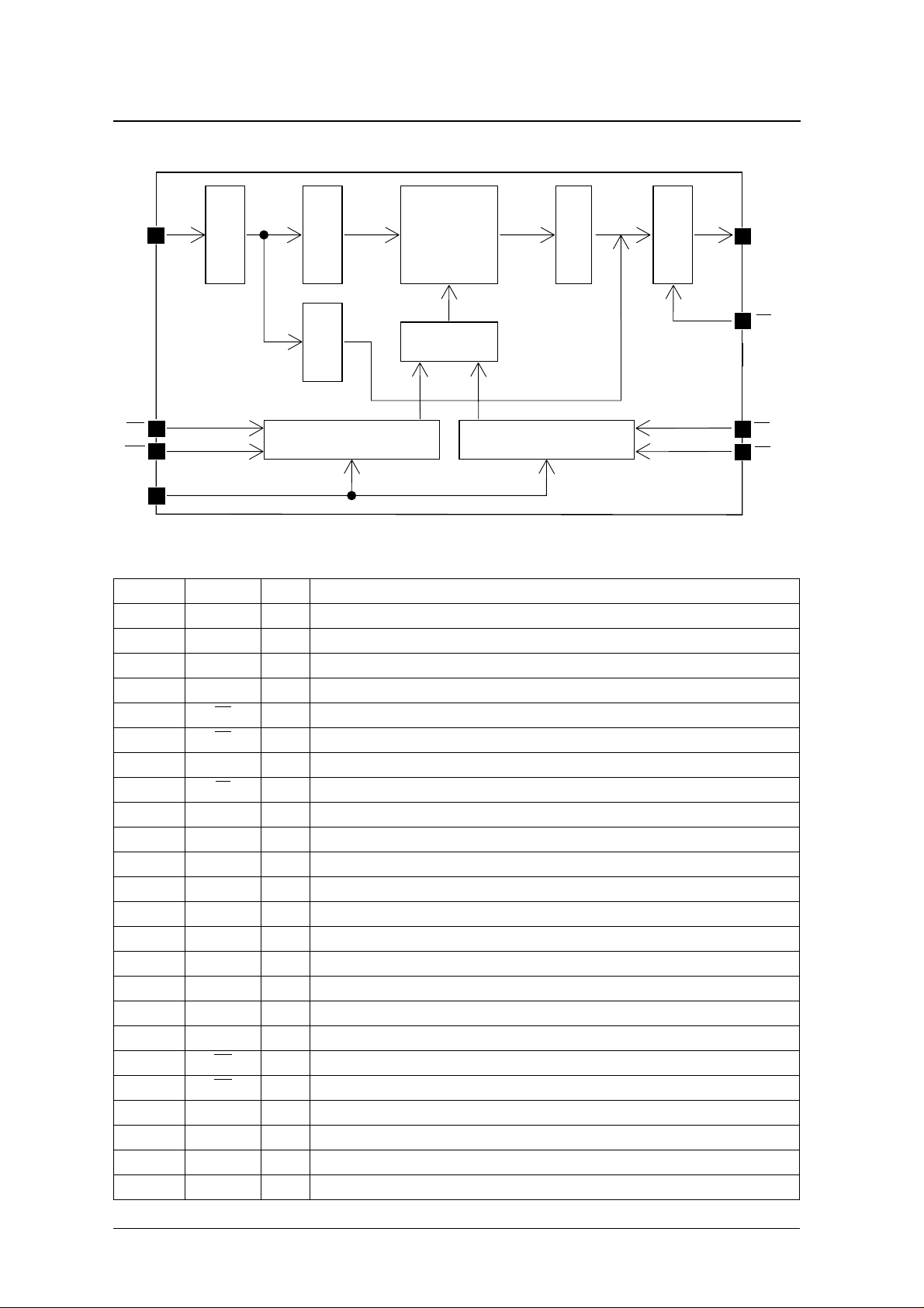
BLOCK DIAGRAM
SM5838AS
DIN
8
8
Input buffer
32 32 8
SRAM
S/P converter
Decoder
Cache
WE
RW
CLK
Write address pointer Read address pointer
PIN DESCRIPTION
Number Name I/O Function
1 DOUT0 O Read data output bit 0
2 DOUT1 O Read data output bit 1
3 DOUT2 O Read data output bit 2
4 DOUT3 O Read data output bit 3
5OE
6RRI Reset read input
7 VSS – Ground (0 V) pin
8REI Read enable input (read address pointer)
9 DOUT4 O Read data output bit 4
10 DOUT5 O Read data output bit 5
11 DOUT6 O Read data output bit 6
12 DOUT7 O Read data output bit 7
13 DIN7 I Write data input bit 7
14 DIN6 I Write data input bit 6
15 DIN5 I Write data input bit 5
16 DIN4 I Write data input bit 4
17 CLK I Clock input
18 VDD – Supply pin
19 RW I Reset write input
20 WE I Write enable input (write address pointer)
21 DIN3 I Write data input bit 3
22 DIN2 I Write data input bit 2
23 DIN1 I Write data input bit 1
24 DIN0 I Write data input bit 0
I Output enable input
P/S converter
8
Output buffer
DOUT
OE
RE
RR
NIPPON PRECISION CIRCUITS—2
Page 3
−
−
−
°
°
−
° C
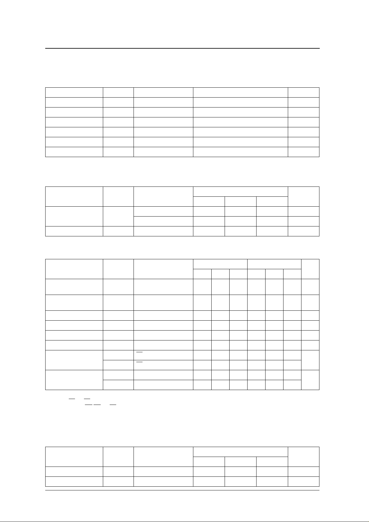
SPECIFICATIONS
Absolute Maximum Ratings
V
= 0 V
SS
Parameter Symbol Condition Rating Unit
Supply voltage range V
Input voltage range V
Storage temperature range T
Power dissipation P
Soldering temperature T
Soldering time t
Recommended Operating Conditions
DD
IN
stg
D
sld
sld
µ
SM5838AS
0.3 to 7.0 V
V
SS
0.3 to V
+ 0.3 V
DD
40 to 125
C
500 mW
255
C
10 s
V
= 0 V
SS
Parameter Symbol Condition
min typ max
Normal-voltage specification 4.5 5.0 5.5 V
Supply voltage range V
Operating temperature T
DD
opr
Low-voltage specification 3.0 3.3 4.5 V
20 – 70
DC Characteristics
Parameter Symbol Condition
Operating current
consumption
Standby current
consumption
Input leakage current
Input leakage current
Input voltage
Input voltage
Output high-impedance
leakage current
Output voltage
2
3
2
3
4
4
I
DD
I
ST
I
LH
I
LL
V
V
I
ZH
I
ZL
V
OH
V
OL
IH
IL
No output load
V
= V
IN
V
= 0 V ––1––1 µ A
IN
OE
= HIGH, V
OE
= HIGH, V
I
= − 1 mA 2.5 – – 2.0 – –
OH
I
= 2 mA – – 0.4 – – 0.8
OH
1
DD
= V
OUT
DD
= 0 V ––5––5
OUT
1. Normal-voltage specification (CLK = 33.3 MHz); Low-voltage specification (CLK = 20 MHz, V
2. Pins CLK, RR
and RE.
3. Pins DIN0 to DIN7, RW, WE and OE.
4. Pins DOUT0 to DOUT7.
5 V supply 3 V supply
min typ max min typ max
–7590–2230mA
––50––50 µ A
––1––1 µ A
2.4 – – 2.0 – – V
– – 0.5 – – 0.5 V
––5––5
= 3.3 ± 0.3 V)
DD
Rating
Unit
Unit
A
V
Input/Outputs
Ta = 25 ° C, f = 1 MHz
Parameter Symbol Condition
Input capacitance C
Output capacitance C
Rating
Unit
min typ max
I
O
– – 10 pF
– – 10 pF
NIPPON PRECISION CIRCUITS—3
Page 4
AC Characteristics
,,,,,,
,,,,,,
,,,,,,
Input timing
SM5838AS
Parameter Symbol Condition
5 V supply 3 V supply
min typ max min typ max
Clock cycle time t
Clock pulsewidth t
CKW
Input data setup time t
Input data hold time t
R
W and RR setup time t
R
W and RR hold time t
WE
setup time t
WE
hold time t
RE
setup time t
RE
hold time t
OE
setup time t
OE
hold time t
WES
WEH
RES
REH
OES
OEH
Rise and fall transition times t
1. All voltages measured with relative to V
2. Input timing input voltage levels are V
3. Input signal reference level is V
4. Input timing ratings measured with t
= 1.5 V.
TH
IL
= 5 ns.
T
CK
DS
DH
RS
RH
T
.
SS
= 0 V and V
= 3.0/2.5 V (5/3 V supply). Transition time is measured between V
IH
30 – – 50 – – ns
13 – – 23 – – ns
7––10––ns
3––4––ns
10 – – 17 – – ns
0––0––ns
13 – – 23 – – ns
0––0––ns
13 – – 23 – – ns
0––0––ns
10 – – 17 – – ns
0––0––ns
– – 30 – – 30 ns
Normal-voltage (5 V) specification Low-voltage (3 V) specification
IH
and V
Unit
.
IL
3.0V
0V
CLK
RW
RR
WE
RE
OE
5ns 5ns
t
CK
t
CKW
t
CKW
t
RS
t
RH
t
RS
t
RH
t
t
OEH
OES
2.5V
0V
5ns 5ns
t
RW
t
RR
t
WEH
t
REH
t
WES
t
RES
t
RH
t
RS
t
RH
t
RS
t
WEH
t
t
OEH
t
WES
t
REH
RES
t
OES
DIN
t
t
t
DS
DH
DS
t
DH
NIPPON PRECISION CIRCUITS—4
Page 5
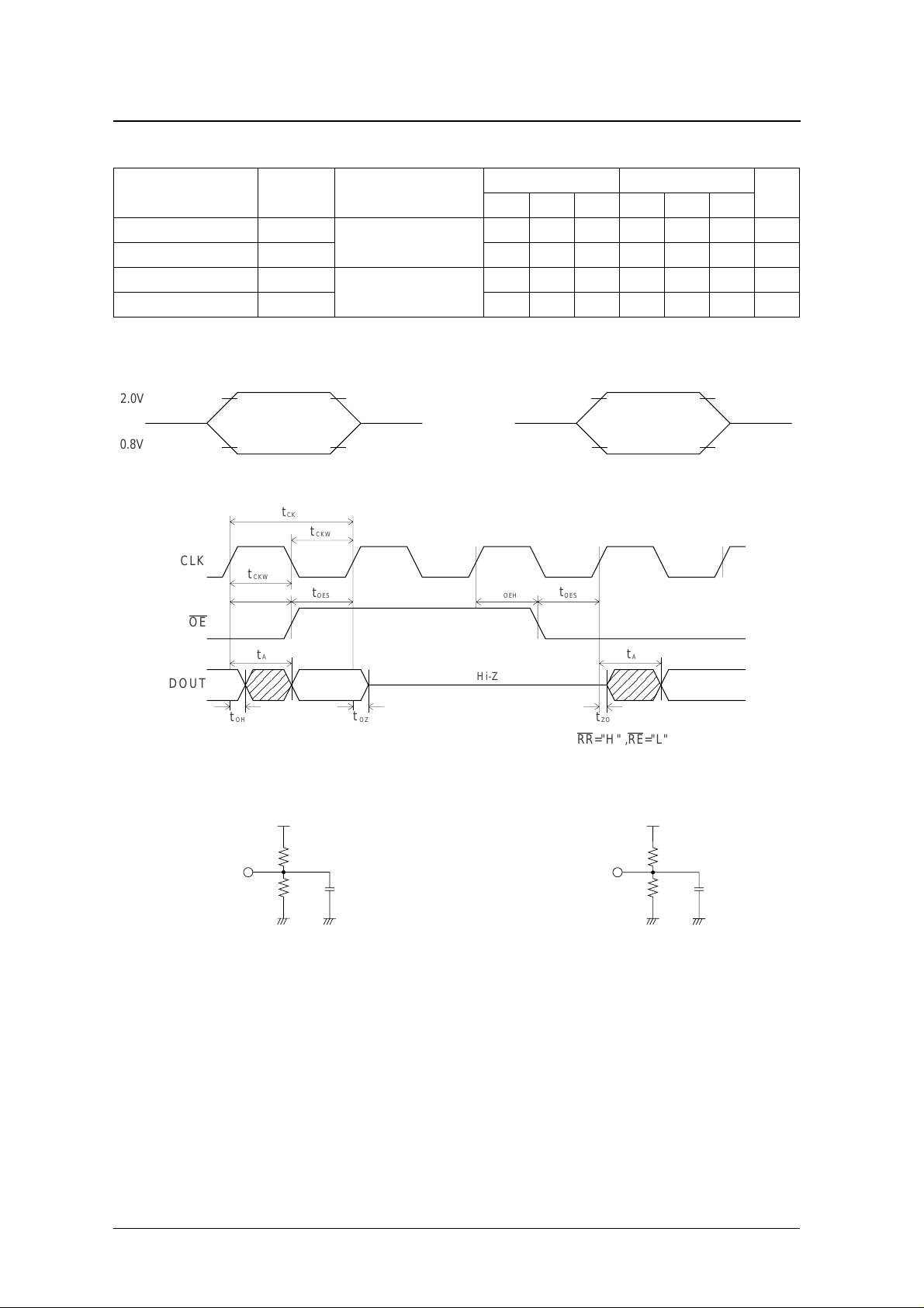
Output timing
SM5838AS
Parameter Symbol Condition
5 V supply 3 V supply
min typ max min typ max
Access time t
Output hold time t
Output enable delay time
Output disable delay time
1. t
and t
ZO
are measured with ± 200 mV tolerance.
OZ
1
1
A
OH
t
ZO
t
OZ
“Load circuit 1”
“Load circuit 2”
– – 20 – – 40 ns
5––5––ns
5 – 27 5 – 40 ns
5 – 27 5 – 40 ns
Normal-voltage (5 V) specification Low-voltage (3 V) specification
2.0V
0.8V
t
CK
t
CKW
1.8V
1.0V
CLK
t
CKW
t
OEH
t
OES
t
OEH
t
OES
OE
Unit
t
A
DOUT
t
OH
t
OZ
Hi-Z
Load circuit 1 Load circuit 2
VDD
1.8k
Ω
DOUT
Ω
1.1k
30pF
t
A
t
ZO
RR="H" ,RE="L"
DOUT
VDD
1.8k
1.1k
Ω
Ω
5pF
NIPPON PRECISION CIRCUITS—5
Page 6

SM5838AS
FUNCTIONAL DESCRIPTION
At power-ON reset, device operation can become
irregular during the interval when the control circuits
are being reset. After power-ON reset is released,
this can take up to several 10s of ms in some cases.
Write Reset Cycle, Read Reset Cycle
After power-ON, the write address pointer and read
address pointer positions are undefined. Accordingly,
it is necessary to initialize the pointers using a write
reset cycle and read reset cycle, respectively.
A write reset cycle (read reset cycle) is valid when
RW (RR) goes LOW for an interval that satisfies
Write reset cycle
n cycle reset cycle 0 cycle 1 cycle
t
CKW
CLK
t
CKW
t
t
RS
RW
RW
t
RH
t
DS
(n-1) (n) (1)(0)
DIN
t
DH
Read reset cycle
both the CLK rising edge setup time (t
time (t
). Note that a write reset cycle (read reset
RH
) and hold
RS
cycle) can occur simultaneously with a write cycle
(read cycle). If the cycles are not simultaneous, then
the write reset cycle (read reset cycle) is completed
at the start of the next write cycle (read cycle).
t
RH
t
RS
t
DS
t
DH
WE="L"
n cycle reset cycle 0 cycle 1 cycle
t
CKW
CLK
RR
DOUT
Note the even if a reset period (t
t
CKW
t
RS
t
RH
t
A
(n-1) (n) (1)(0)
RW
t
t
, t
A
OH
) is zero
RR
t
RR
length in the write reset and read reset cycles, the
reset operation does take place.
(0)
t
RH
t
RS
t
A
t
OH
t
A
t
OH
RE="L" , OE="L"
NIPPON PRECISION CIRCUITS—6
Page 7

Write Cycle
SM5838AS
The input data address is determined by the write
address pointer position. The write address pointer is
reset by RW (write reset cycle), and is incremented
on the rising edge of CLK whenever WE is LOW.
n cycle n+2 cycle disable cycle n+1 cycle
t
CKW
CLK
t
CKW
t
WEH
t
WES
WE
t
t
DS
DIN
(n-1) (n) (n+1) (n+2)
t
DH
DS
Read Cycle
The output data address is determined by the read
address pointer position. The read address pointer is
reset by RR (read reset cycle), and is incremented on
the rising edge of CLK whenever RE is LOW. Data
output starts t
the start of the read cycle and continues until t
(min) after the next rising edge of CLK.
(max) after the rising edge of CLK at
A
OH
Data input occurs on the rising edge of CLK at the
end of the write cycle.
When WE goes HIGH, write operation is disabled
and the write address pointer stops.
t
WEH
t
DH
t
WES
RW="H"
When RE goes HIGH, read operation is disabled and
the read address pointer stops.
Note that data being read was written at least 20
write cycles previously (FIFO minimum delay).
Therefore, if (write address pointer) − (read address
pointer) = 1 to 19, then a possibility exists that data
from the preceding line is output instead.
CLK
RE
DOUT
n cycle n+2 cycle disable cycle n+1 cycle
t
CKW
t
CKW
t
REH
t
A
(n-1) (n) (n+1) (n+2)
t
A
t
OH
t
RES
t
REH
t
RES
t
A
t
OH
RR="H" , OE="L"
NIPPON PRECISION CIRCUITS—7
Page 8

SM5838AS
,,
,,
,,
,,
,,
,,
,,
,,
Output Enable
When OE is HIGH, DOUT0 to DOUT7 become high
impedance. Note that because RE operation is independent of OE operation, the read address pointer
can be incremented even when the outputs are high
impedance.
n cycle n+3 cycle n+2 cycle n+1 cycle
t
CKW
CLK
t
CKW
t
OEH
t
OES
OE
t
A
(n-1)
DOUT
(n) (n+3)
t
OZ
TYPICAL APPLICATIONS
Note that at power-ON, the write address pointer and
read address pointer positions are undefined.
Accordingly, RW and RR reset cycles are required.
1H Delay Line
A 5120-word delay line can be realized by performing simultaneous write reset and read reset at powerON.
An n-word delay line (21 to 5210-word) can be realized using any of the following methods.
t
OEH
t
OES
t
A
Hi-Z
t
ZO
RR="H" ,RE="L"
1. Perform reset in sync with desired delay length.
2. Stagger RW and RR timing to desired delay
length.
3. Manipulate the write or read address pointer
using WE or RE to disable incrementing to
maintain sync with desired delay length.
1H (5120-word) delay line timing
0 cycle 2 cycle 1 cycle
CLK
t
t
RS
RH
RW
RR
t
t
DS
DH
DIN
DOUT
0 5119 5118
1
5120 cycle
1H
2
5119
cycle
5120+0
cycle
t
A
5120+1
cycle
t
OH
0 1 2
2H
5120+2
cycle
5120+3
cycle
3 0 1 2
3
WE="L" , RE="L" , OE="L"
NIPPON PRECISION CIRCUITS—8
Page 9

n-word delay line timing 1
1H
SM5838AS
2H
0 cycle 2 cycle 1 cycle
CLK
t
t
RS
RH
RW
RR
t
t
DS
DH
DIN
0 n-2 n-1
DOUT
n-word delay line timing 2
0 cycle 2 cycle 1 cycle
CLK
t
t
RS
RH
RW
1
n cycle
1H
2
n-1
cycle
n-1
cycle
n+0
cycle
t
A
n+1
cycle
t
OH
0 1 2
n+2
cycle
n+3
cycle
3 0 1 2
3
WE="L" , RE="L" , OE="L"
2H
n+0
cycle
t
t
RS
RH
n+1
cycle
n+2
cycle
n+3
cycle
RR
t
t
DS
DH
DIN
0 n-2
DOUT
n-word delay line timing 3
0 cycle 2 cycle 1 cycle
CLK
t
t
RS
RH
RW
RR
RE
t
t
DS
DH
DIN
0 n-2 n-1
n cycle
1H
2 1
n-1
t
t
OH
A
0 1 2
3 0 1 2
3
WE="L" , RE="L" , OE="L"
2H
n-1
cycle
2 1
n+0
cycle
t
RES
n+1
cycle
n+2
cycle
n+3
cycle
3 0 1 2
DOUT
n cycle
t
t
A
OH
0 1 2
3
WE="L" , RE="L" , OE="L"
NIPPON PRECISION CIRCUITS—9
Page 10

High-speed Conversion
SM5838AS
For example, an NTSC signal interlace-to-noninterlace conversion. If interpolated line data can be
assumed to be similar to the preceding line data and
the write data rate is 14.3 MHz (4f
), then conver-
SC
sion can be realized by reading twice at 28.6 MHz
(8f
).
SC
Furthermore, interpolated line data, with appropriate
signal processing separation, can be read out line-by-
Preceding line data used as interpolated line
WE
RE
OE
RR
012345 012
nH nH+1H
012 012909 909
nH-1H nH nH nH+1H
012345
012345
909
*Output data 867 to 909 forms the preceding 1H data.
CLK
RW
DIN
DOUT
line by alternating between 2 SM5838AS devices (1
line/device).
In reality, however, double the number of devices are
required for luminance signal (Y) and color difference signal (C) systems. And triple the number of
devices are required for RGB signal systems.
1819
012345
909 *
012345
909
909 *
Interpolated data used as interpolated line
CLK
(A)DIN
(B)DIN
(A)RE
(A)OE
(A)RR
(A)DOUT
(B)RE
(B)OE
(B)RR
(B)DOUT
012345
WE
RW
nH nH+1H
012 012909 909
nH' nH'+1H
012 012909 909
012345
nH'-1H nH'
012345 012345
909
*Output data 867 to 909 forms the preceding 1H data.
1819
012
nH nH+1H
012345
909 * 909 *
909
NIPPON PRECISION CIRCUITS—10
Page 11

SM5838AS
1/2 Data Reduction
Input data rate reduction by half can be realized by
taking WE and RE simultaneously HIGH only once
every two clock cycles.
Noninterlace-to-interlace conversions line extraction
can be realized by switching WE LO W/HIGH in line
units and RE LOW/HIGH in word units.
1/2 data reduction
5119
5119
CLK
WE
RW
DIN
RE
OE
RR
DOUT
012345 012
nH nH+1H
012345 012345
024
7 8 96 7 8 96
nH-1H nH
6 10 12 148 5118 0 2 4 6 10 12 148 5118
1/2 line extraction (noninterlace-to-interlace conversion)
1819
CLK
WE
RW
DIN
012345 012
nH-1H nH+1H
012345 012345
909
RE
nH nH+2H
2345 234501 01
5119
909909 909
OE
RR
DOUT
nH-2H nH
012 012909 909
NIPPON PRECISION CIRCUITS—11
Page 12

SM5838AS
1/2n data reduction (n × n pixel reduction)
Screen resolution reduction, or 2 × 2 pixel reduction,
can be realized by combining both 1/2 data reduction
and 1/2 line extraction schemes. Furthermore, n × n
pixel reduction (for integer n) can be realized by
changing the WE and RE disable intervals and the
RW and RR reset timing.
2 × 2 pixel reduction (1/4 reduction)
2 pixels
Valid
2 pixels
CLK
WE
RW
DIN
RE
012345
012345 012345
Invalid
Invalid
Invalid
909
nH-1H nH+1H
909
nH nH+2H
2345 234501 01
Also, if the same data is repeatedly read out in place
of other data that has been discarded, the screen resolution can be reduced without changing the data rate
to realize a mosaic filter function.
909909 909
OE
RR
DOUT
02 02908 908
2 × 2 pixel reduction (mosaic)
2 pixels
2 pixels
CLK
WE
RW
DIN
RE
Valid
012345
nH-1H nH+1H
012345 012345
nH-2H nH
909
nH nH+2H
2345 234501 01
909
909
909909
OE
RR
DOUT
nH-2H
024
nH-2H nH
6 908* 6
024
908 0 2 4 908* 0 2 4 908
nH
*Output date 902 to 908 forms the preceding 1H data.
NIPPON PRECISION CIRCUITS—12
Page 13

SM5838AS
Wipe Function (Screen Switching)
Because RE and OE operate independently, a screen
wipe function can be realized using 2 SM5838AS
devices by switching OE LOW/HIGH in field units.
Screen wipe (OE changes in field units)
CLK
RW
(A)DIN 012345
(B)DIN
(A)RE
(A)OE
(A)RR
(A)DOUT
(B)RE
012345
WE
012345
nH-1H nH nH+1H
nH'-1H nH' nH'+2H
nH-2H nH
45
909
012345 012345 012345
909
012345 012345 012345
909
nH-1H nH+1H
45
909
nH+2H
909 909
nH'+1H
909 909
45
909
909
45
909 909 909
(B)OE
(B)RR
(B)DOUT
123
0
nH'-2H nH'nH'-1H nH'+1H
0123
0123
0123
Screen wipe image (left to right)
(A)(B)
NIPPON PRECISION CIRCUITS—13
Page 14

SM5838AS
NIPPON PRECISION CIRCUITS INC. reserves the right to make changes to the products described in this data sheet in order to
improve the design or performance and to supply the best possible products. Nippon Precision Circuits Inc. assumes no responsibility for
the use of any circuits shown in this data sheet, conveys no license under any patent or other rights, and makes no claim that the circuits
are free from patent infringement. Applications for any devices shown in this data sheet are for illustration only and Nippon Precision
Circuits Inc. makes no claim or warranty that such applications will be suitable for the use specified without further testing or modification.
The products described in this data sheet are not intended to use for the apparatus which influence human lives due to the failure or
malfunction of the products. Customers are requested to comply with applicable laws and regulations in effect now and hereinafter,
including compliance with export controls on the distribution or dissemination of the products. Customers shall not export, directly or
indirectly, any products without first obtaining required licenses and approvals from appropriate government agencies.
NIPPON PRECISION CIRCUITS INC.
4-3, 2-chome Fukuzumi
Koto-ku, Tokyo 135-8430, Japan
NIPPON PRECISION CIRCUITS INC.
Telephone: 03-3642-6661
Facsimile: 03-3642-6698
NC9411AE 1996.09
NIPPON PRECISION CIRCUITS—14
 Loading...