

Page 1
SM5837AF
NIPPON PRECISION CIRCUITS INC.
OVERVIEW
The SM5837AF is a variable-length delay line LSI.
It has 12-bit input/output signal which can be set to
undergo a delay in the range of 31 to 2078 delay bits.
Maximum operating frequency is 40 MHz, making it
ideal for use in video signal processing applications.
FEATURES
■
Variable-length 1H delay
■
12-bit input/output signal width
■
31 to 2078- bit delay length range
■
40 MHz maximum operating frequency
■
Selectable delay setting method
• 11-bit parallel input
• 3-line serial input
■
TTL-compatible input/outputs
■
Tristate outputs
■
4.75 to 5.25 V operating voltage
■
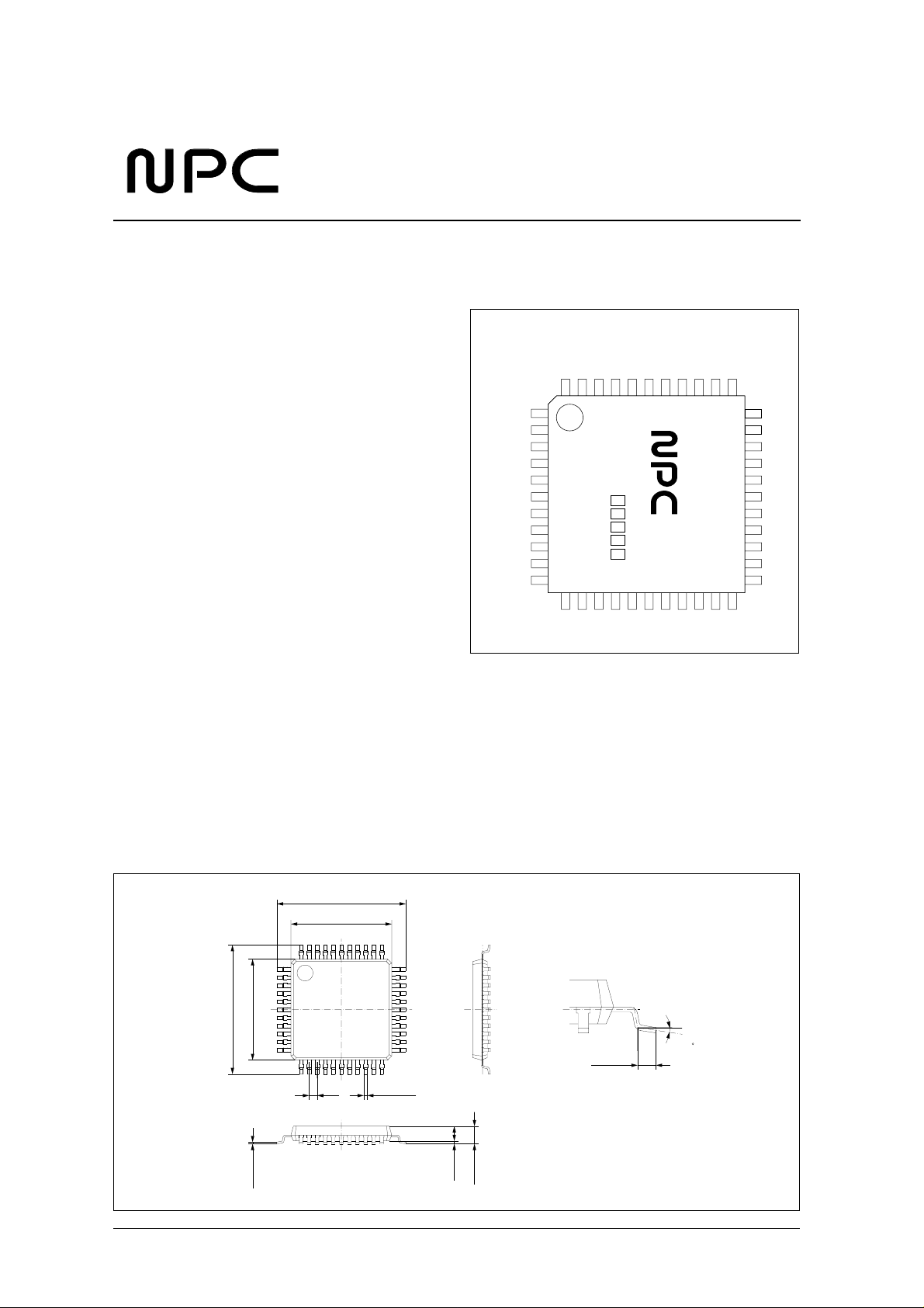
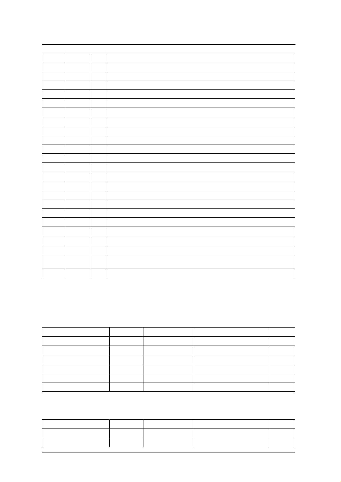
44-pin QFP
■
Molybenum-gate CMOS process
Variable-length 1H Delay Line LSI
PINOUT
TOP VIEW
RSTN
(NC)
PARA
DI0
DI1
DI2
DI3
DI4
DI5
DI6
DI7
34
35
36
37
38
39
40
41
42
43
44
DO8
(NC)
33
DI8
32
DI9
31
DI10
30
DI11
29
OE
28
CLK
27
VDD
26
DO11
25
DO10
24
DO9
23
DO8
DL0/SDI
DL1/SICK
DL2/LEN
DL3
DL4
VSS1
DL5
DL6
DL7
DL8
DL9
1
2
3
4
5
6
7
8
9
10
11
1213141516171819202122
DL10
DO0
DO1
DO2
SM5837AF
DO3
VSS2
DO4
DO5
DO7
APPLICATIONS
■
Video signal image processing
PACKAGE DIMENSIONS
Unit: mm
44-pin QFP
-
+
10.00
12.80 0.30
+
12.80 0.30
-
10.00
0.80
+
0.35 0.10
-
+
0.60 0.20
-
0 to 10
+
-
0.17 0.05
0 to 0.20 1.45
1.75MAX
NIPPON PRECISION CIRCUITS—1
Page 2

BLOCK DIAGRAM
SM5837AF
DI0 - 11
12 12 12
CLK
RSTN
PARA
SDI
SICK
LEN
Variable-length
12-bit
1H Delay
Delay Length Control
11
Parallel/Serial Select
11
SIPO
DL0 - 10
Output Buffer
11
PIN DESCRIPTION
Number Name I/O
1 DL0/SDI Ip Delay length set parallel data bit DL0 (LSB) when PARA is HIGH, and SDI serial data input when PARA is LOW.
2 DL1/SICK Ip Delay length set parallel data bit DL1 (bit 1) when PARA is HIGH, and SICK shift clock when PARA is LOW.
3 DL2/LEN Ip Delay length set parallel data bit DL2 (bit 2) when PARA is HIGH, and LEN latch clock when PARA is LOW.
4 DL3 Ip Delay length set data bit 3
5 DL4 Ip Delay length set data bit 4
6 VSS1 – Ground (0 V) pin 1
7 DL5 Ip Delay length set data bit 5
8 DL6 Ip Delay length set data bit 6
9 DL7 Ip Delay length set data bit 7
10 DL8 Ip Delay length set data bit 8
11 DL9 Ip Delay length set data bit 9
12 DL10 Ip Delay length set data bit 10
13 DO0 O Signal output data bit 0
14 DO1 O Signal output data bit 1
15 DO2 O Signal output data bit 2
16 DO3 O Signal output data bit 3
17 VSS2 – Ground (0 V) pin 2
18 DO4 O Signal output data bit 4
19 DO5 O Signal output data bit 5
20 DO6 O Signal output data bit 6
21 DO7 O Signal output data bit 7
(1)
Function
DO0 - 11
OE
VDD
VSS2
VSS1
NIPPON PRECISION CIRCUITS—2
Page 3
−
−
−
°
°
−
° C
SM5837AF
Number Name I/O
22 NC – No connection
23 DO8 O Signal output data bit 8
24 DO9 O Signal output data bit 9
25 DO10 O Signal output data bit 10
26 DO11 O Signal output data bit 11
27 VDD – Supply (5 V) pin
28 CLK I Clock input
29 OE Ip Tristate output enable. Enable when HIGH, and disable when LOW.
30 DI11 Ip Signal input data bit 11
31 DI10 Ip Signal input data bit 10
32 DI9 Ip Signal input data bit 9
33 DI8 Ip Signal input data bit 8
34 DI7 Ip Signal input data bit 7
35 DI6 Ip Signal input data bit 6
36 DI5 Ip Signal input data bit 5
37 DI4 Ip Signal input data bit 4
38 DI3 Ip Signal input data bit 3
39 DI2 Ip Signal input data bit 2
40 DI1 Ip Signal input data bit 1
41 DI0 Ip Signal input data bit 0
42 RSTN Ip Reset pin. Normal operation when HIGH, and reset operation when LOW.
43 PARA Ip
44 NC – No connection
(1)
Delay length setting method select.
Parallel data (DL0 to DL10) when HIGH, and serial input (SDI, SICK, LEN) when LOW.
Function
1. Ip = input pin with built-in pull-up resistor, O = output.
SPECIFICATIONS
Absolute Maximum Ratings
V
= V
SS
Supply voltage range V
Input voltage range V
Storage temperature range T
Power dissipation P
Soldering temperature T
Soldering time t
Recommended Operating Conditions
V
= 0 V
SS
Supply voltage range V
Operating temperature T
= V
SS1
Parameter Symbol Condition Rating Unit
Parameter Symbol Condition Rating Unit
SS2
= 0 V
DD
IN
stg
D
sld
sld
DD
opr
0.3 to 7.0 V
V
0.3 to V
SS
4.75 to 5.25 V
+ 0.3 V
DD
40 to 125
450 mW
255
10 s
20 to 70
C
C
NIPPON PRECISION CIRCUITS—3
Page 4

DC Characteristics
V
= 4.75 to 5.25 V, V
DD
= 0 V, T
SS
µ
µ
SM5837AF
= − 20 to 70 ° C unless otherwise specified
a
µ A
Parameter Symbol Condition
V
= 5.0 V, CLK frequency
Current consumption I
(1)
Input voltage
Output voltage
Input current
Input leakage current
Input leakage current
Output high-impedance leakage
current
(2)
(3)
(2)
(1) (2)
(1)
(3)
DD
V
IH
V
IL
V
OH
V
OL
I
IL
I
LH
I
LL
I
ZH
I
ZL
DD
f
= 40 MHz, OE = 0 V
C
I
= − 0.4 mA 4.0 – – V
OH
I
= 1.6 mA – – 0.4 V
OL
V
= 0 V – 10 20
IN
V
= V
IN
DD
V
= 0 V – – 1
IN
V
= V
OUT
DD
V
= 0 V – – 5
OUT
1. Pin CLK.
2. Pins DI0 to DI11, PARA, DL0/SDI, DL1/SICK, DL2/LEN, DL3 to DL10, OE and RSTN.
3. Pins DO0 to DO11.
AC Characteristics
V
= 4.75 to 5.25 V, V
DD
= 0 V, T
SS
= − 20 to 70 ° C unless otherwise specified
a
Rating
Unit
min typ max
– – 85 mA
2.4 – – V
– – 0.5 V
A
––1 µ A
A
––5 µ A
Parameter Symbol Condition
CLK clock cycle t
CLK clock HIGH-level pulsewidth t
CLK clock LOW-level pulsewidth t
SICK clock cycle t
SICK clock HIGH-level pulsewidth t
SICK clock LOW-level pulsewidth t
CLK, SICK and LEN rise time t
CLK, SICK and LEN fall time t
DI0 to DI11, DL0 to DL10 and RSTN
setup time
DI0 to DI11, DL0 to DL10 and RSTN
hold time
SDI setup time t
SD1 hold time t
SICK rising edge → LEN rising edge t
LEN rising edge → SICK rising edge t
CLK → DO0 to D011 output delay t
CLK → DO0 to D011 output hold time t
OE HIGH-level pulsewidth t
OE LOW-level pulsewidth t
CP1
CH1
CL1
CP2
CH2
CL2
CR
t
t
CE
EC
PD
OH
OEH
OEL
Rating
Unit
min typ max
25 – – ns
10 – – ns
10 – – ns
50 – – ns
20 – – ns
20 – – ns
1.0 to 2.0 V – – 10 ns
CF
S1
H1
S2
H2
1.0 to 2.0 V – – 10 ns
10 – – ns
0––ns
25 – – ns
25 – – ns
25 – – ns
25 – – ns
– – 20 ns
See “Load conditions 1”.
5––ns
50 – – ns
50 – – ns
NIPPON PRECISION CIRCUITS—4
Page 5

SM5837AF
Parameter Symbol Condition
t
t
t
PZH
t
PHZ
PZL
PLZ
IN
OUT
See “Load conditions 2”.
f = 1 MHz – – 10 pF
f = 1 MHz, OE = V
IL
OE → DO0 to DO11 output enable
delay
OE → DO0 to DO11 output disable
delay
Input capacitance C
Output capacitance C
Load conditions 1 Load conditions 2
OUTPUT
OUTPUT
40pF
t
CLK
CR
2.0V
1.0V
t
CF
t
CH1
t
t
CL1
CP1
Rating
min typ max
– – 25 ns
– – 25 ns
– – 25 ns
– – 25 ns
– – 15 pF
500
Ω
40pF
0V( )
2.6V( )
,
t
PHZ
,
t
PLZ
2.4V Min
1.5V
0.5V Max
Unit
t
PZH
t
PZL
CLK
DI0 - 11
DL0 - 10
RSTN
CLK
DO0 - 11
t
S1
t
S1
t
S1
VALID
1.5V
t
H1
1.5V
t
H1
1.5V
t
H1
1.5V
1.5V
t
PD
t
OH
VALID
1.5V
NIPPON PRECISION CIRCUITS—5
Page 6

SM5837AF
OE
DO0 - 11
SDI
Hi-Z
Hi-Z
t
OEH
t
PZH
t
PZL PLZ
t
CP2
t
CL2
t
S2
t
CH2
t
H2
t
CE
t
OEL
1.5V
t
PHZ
0.5V
1.5V
t
0.5V
1.5V
1.5VSICK
1.5V
t
EC
LEN 1.5V
FUNCTIONAL DESCRIPTION
Parallel Input Set Method
The SM5837AF provides a built-in 1H delay for
video signal processing. The delay can be set to a
length of 31 to 2078 clock delay bits. The delay
length (L
) can be set using 2 methods, selected by
H
the state of PARA. When PARA is HIGH, the delay
length is set by parallel input data on DL0 to DL10.
When PARA is LOW, the delay length is set by serial
input data using SDI, SICK and LEN. Accordingly,
the function of DL0/SDI, DL1/SICK and DL2/LEN
is determined by PARA.
Table 1. Delay bit length setting
DL10 DL9 DL8 DL7 DL6 DL5 DL4 DL3 DL2 DL1 DL0 Delay length
00000000000 31
00000000001 32
00000000010 33
(PARA, DL0 to DL10)
When PARA is HIGH, parallel input data is used to
set the delay length. The delay length (L
mined by the input data on DL0 to DL10 as shown in
equation 1 and table 1.
10
31 DLk 2k×{}
+=
H
∑
k0=
) is deter-
H
(1)L
00000000011 34
00000000100 35
↓↓↓↓↓↓↓↓↓↓↓ ↓
00111100001 512
NIPPON PRECISION CIRCUITS—6
Page 7

SM5837AF
Table 1. Delay bit length setting
DL10 DL9 DL8 DL7 DL6 DL5 DL4 DL3 DL2 DL1 DL0 Delay length
00111100010 513
↓↓↓↓↓↓↓↓↓↓↓ ↓
01111100001 1024
01111100010 1025
↓↓↓↓↓↓↓↓↓↓↓ ↓
11111100001 2048
11111100010 2049
↓↓↓↓↓↓↓↓↓↓↓ ↓
11111111110 2077
11111111111 2078
Serial Input Set Method
(PARA, SDI, SICK, LEN)
When PARA goes LOW, 3-input serial data set
method is used to set the delay length. Inputs DL3 to
DL10 are ignored. SDI, SICK and LEN function as
the serial data input, serial data shift clock and latch
clock enable, respectively.
The serial input data format, shown in figure XREF,
comprises 11-bit serial data (S0 to S10) input on SDI
in sync with SICK. The data on SDI is clocked into
S10 S9 S8 S7 S6 S5 S4 S3 S2 S1 S0SDI
SICK
LEN
Dotted lines indicate possible SICK and LEN states.
the serial-to-parallel converter shift register on the
rising edge of SICK, and 11-bit parallel data is then
latched into the delay length set register on the rising
edge of LEN.
The delay length (L
) is determined by the input
H
data S0 to S10 (just as for parallel input data DL0 to
DL10) as shown in equation 2. See also table 1.
Note that SICK and CLK can be asynchronous.
10
31 Sk 2k×{}
+=
H
∑
k0=
(2)L
Figure 1. Serial input data format
Delay Clock Input (CLK)
All 1H delay registers operate in sync with the delay
clock CLK. The maximum clock frequency is 40
MHz.
Input Data (DI0 to DI11)
DI0 to DI11 are the 12-bit data inputs.
Output Data (DO0 to DO11,OE)
DO0 to DO11 are the 12-bit data outputs. They are
tristate outputs, with the output state selected by OE.
When OE is HIGH, the outputs are enabled. When
OE is LOW, the outputs are disabled (high-impedance state).
Reset (RSTN)
At power-ON, the internal timing generator circuits
must be initialized by a LOW-level input on RSTN.
After RSTN goes HIGH, the set delay length
becomes active.
NIPPON PRECISION CIRCUITS—7
Page 8

SM5837AF
TIMING DIAGRAMS
012345 3132333435
CLK
RSTN
D1 D2 D3 D4 D5 D31 D32 D33 D34DI0 - 11
OE
DO0 - 11
Serial Set Data (Delay Length = 32)
DL0/SDI
012345678910
DL1/SICK
DL2/LEN
RSTN
CLK
UNKNOWN
Parallel Set Data (Delay Length = 31)
D35
D1 D2 D3
PARA=H , DL0-10=L
1 2 3 32 33 34
Hi-Z
D5
DI0 - 11
DO0 - 11
INVALID
UNKNOWN
D1 D2 D3
D1 D2 D3
PARA=L , DL3-10=Don't Care , OE=H
NIPPON PRECISION CIRCUITS INC. reserves the right to make changes to the products described in this data sheet in order to
improve the design or performance and to supply the best possible products. Nippon Precision Circuits Inc. assumes no responsibility f or
the use of any circuits shown in this data sheet, conveys no license under any patent or other rights, and makes no claim that the circuits
are free from patent infringement. Applications for any devices shown in this data sheet are for illustration only and Nippon Precision
Circuits Inc. makes no claim or warr anty that such applications will be suitab le for the use specified without further testing or modification.
The products described in this data sheet are not intended to use for the apparatus which influence human lives due to the failure or
malfunction of the products. Customers are requested to comply with applicable laws and regulations in effect now and hereinafter,
including compliance with export controls on the distribution or dissemination of the products. Customers shall not export, directly or
indirectly, any products without first obtaining required licenses and approvals from appropriate government agencies.
NIPPON PRECISION CIRCUITS INC.
NIPPON PRECISION CIRCUITS INC.
4-3, 2-chome Fukuzumi
Koto-ku, Tokyo 135-8430, Japan
Telephone: 03-3642-6661
Facsimile: 03-3642-6698
NC9408AE 1996.01
NIPPON PRECISION CIRCUITS—8
 Loading...