

Page 1
−
SM5170AV
NIPPON PRECISION CIRCUITS INC.
OVERVIEW
The SM5170AV is a PLL synthesizer IC developed
for application in pagers. It incorporates independently-controlled reference frequency and FIN input
frequency dividers, and operates from a low-voltage
FEATURES
■
Supply voltages
•V
= 0.95 to 1.2 V
DD1
(prescaler, counters)
•V
■
FIN input frequency
•f
•f
= 2.0 to 3.3 V (charge pump)
DD2
= 300 MHz (V
FIN
= 330 MHz (V
FIN
= 0.95 V)
DD1
= 1.0 V)
DD1
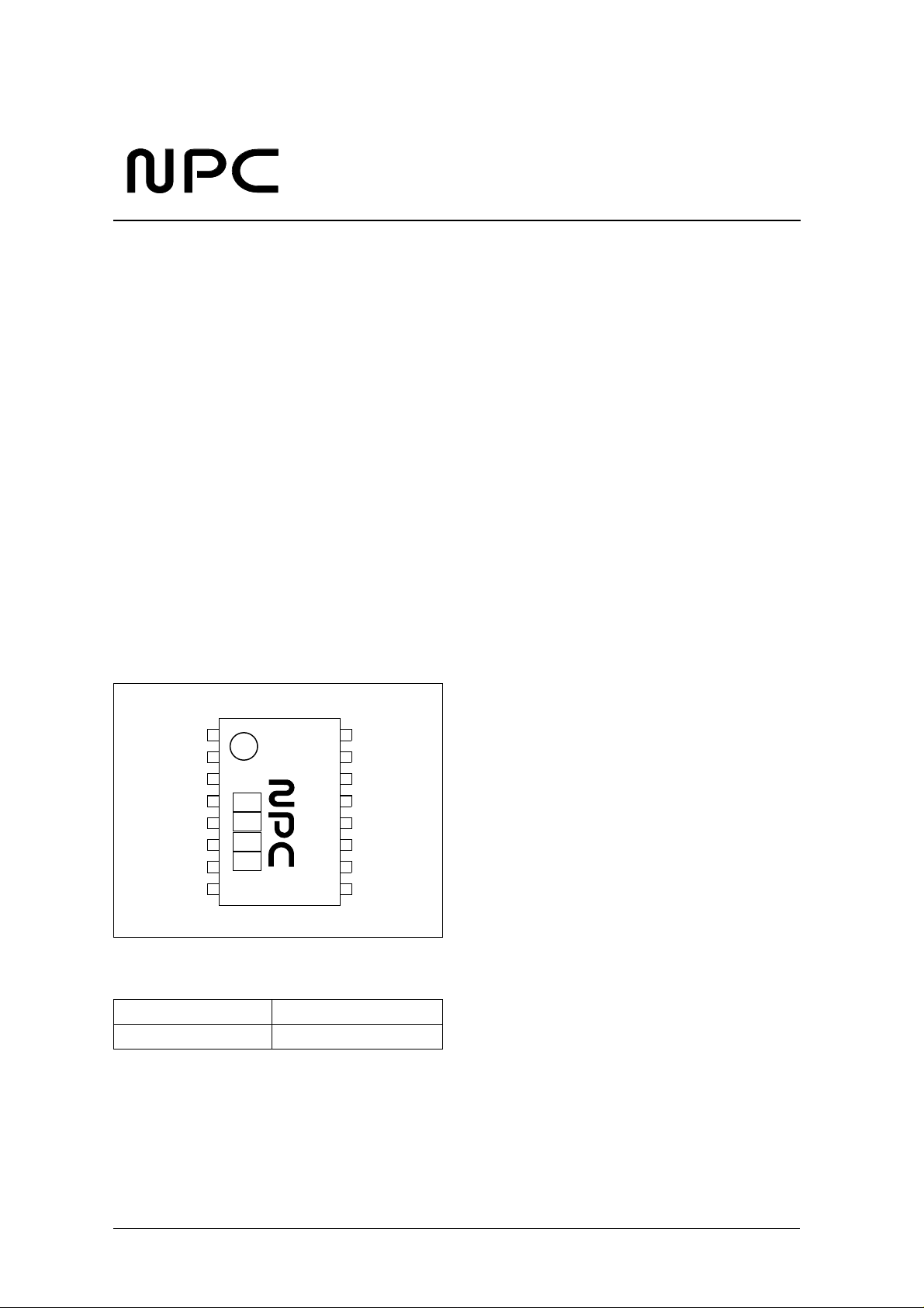
PINOUT
PLL Synthesizer IC
supply to realize low power dissipation. It features a
charge pump that operates at 3 V, making possible a
wide range of VCO designs.
■
Reference frequency
•f
= 25 MHz (V
XIN
■
20 to 262140 reference frequency divider ratio
range (with 1/4 prescaler built-in)
■
1056 to 131071 FIN input frequency divider ratio
range
■
10 to 60 ° C operating temperature range
■
16-pin VSOP
= 0.95 V)
DD1
(Top view)
XIN
XOUT
VDD2
DB
DO
VSS
FIN
VDD1
1
8
16
5170
AV
9
ORDERING INFORMATION
De vice Pack ag e
SM5170AV 16-pin VSOP
TEST
NC
OPR
LE
DATA
CLK
LD
NC
NIPPON PRECISION CIRCUITS—1
Page 2
PACKAGE DIMENSIONS
Unit: mm
16-pin VSOP
SM5170AV
4.4 0.2
6.4 0.2
0.65
BLOCK DIAGRAM
VDD1 AREA(1V)
XIN
XOUT
VDD2 AREA(3V)
CLK
DATA
LE
0.275typ
5.1 0.2
0.10
+ 0.10
0.22
− 0.05
1/4 Prescaler
Latch Selector 22Bit Shift Register
16Bit R−Counter
16Bit R−Latch
0.12
1.15 0.1
0.10 0.05
M
Level
Shifter
0.5 0.2
Boost Signal
Generator
Phase
Detector
0.15
+ 0.10
- 0.05
010
Charge
Pump
DB
DO
OPR
FIN
VDD1 AREA(1V)
Dual Modulus
Prescaler
17Bit N−Latch
5Bit Swallow
Counter
12Bit Main
Counter
Lock
Detector
NIPPON PRECISION CIRCUITS—2
LD
Page 3
−
−
−
−
−
°
−
°
SM5170AV
PIN DESCRIPTION
Number Name I/O Supply Description
1 XIN I 1 V
2 XOUT O 1 V
3 VDD2 – 3 V Phase comparator, charge pump and booster signal 3 V supply
4 D B O 3 V Booster signal output for faster locking
5DOO3 V
6 VS S – – Ground pin
7 FI N I 1 V FIN input frequency divider input pin. Feedback resistor built-in for AC-coupled inputs.
8 VDD1 – 1 V Reference frequency and FIN input frequency prescaler and counter 1 V supply
9 N C – – No connection
10 LD O 1 V
11 CLK I 3 V Control data clock input pin
12 D ATA I 3 V Control data input pin
13 LE I 3 V Control data latch enable signal input pin
14 OPR I 3 V Power-save control pin. Start when HIGH, standby mode when LOW .
15 N C – – No connection
16 TEST I 1 V Test pin. Pull-down resistor built-in. Le av e open or connect to ground for normal operation.
Reference frequency divider cr ystal oscillator connection pins. Alternatively, an external clock input can
be connected to XIN. The clock is output on XOUT. Feedback resistor built-in for AC-coupled inputs.
Phase comparator output pin. Built-in charge pump and tristate output means that this output can be
connected to a low-pass filter. The output polarity is preset for connection to a passive filter.
Unlock signal output pin. (Unlocked when LOW). The function of LD can be turned OFF using the LD
input control bit (LD should be tied LOW when not used).
SPECIFICATIONS
Absolute Maximum Ratings
V
= 0 V
SS
Parameter Symbol Condition Rating Unit
V
Supply voltage
Input voltage range
Storage temperature range T
Po w er dissipation P
V
V
V
DD1
DD2
IN1
IN2
stg
D
Recommended Operating Conditions
V
= 0 V
SS
Parameter Symbol Condition Rating Unit
V
Supply voltage
Operating temperature range T
V
DD1
DD2
opr
VDD1
VDD2
FIN, XIN, TEST V
OPR, CLK, DATA, LE V
VDD1 0.95 to 1.2 V
VDD2 2.0 to 3.3 V
0.3 to 2.0 V
0.3 to 4.6 V
SS
SS
0.3 to V
0.3 to V
+ 0.3 V
DD1
+ 0.3 V
DD2
40 to 125
150 m W
10 to 60
C
C
NIPPON PRECISION CIRCUITS—3
Page 4

Electrical Characteristics
−
−
−
V
= 0 V, V
SS
VDD1 operating current consumption I
VDD2 operating current consumption I
VDD1 standby current I
VDD2 standby current I
FIN maximum operating input frequency f
XIN maximum operating input frequency f
FIN minimum operating input frequency f
XIN minimum operating input frequency f
FIN input amplitude
XIN input amplitude V
OPR, CLK, DATA, LE LOW-level input
voltage
OPR, CLK, DATA, LE HIGH-level input
voltage
FIN LOW -level input current I
XIN LOW -level input current I
FIN HIGH-level input current I
XIN HIGH-level input current I
DB L O W-level output voltage V
DB HIGH-level output voltage V
DO L O W -level output current I
DO HIGH-level output current I
D O , DB tristate output high-impedance
leakage current
DATA → CLK setup time t
CLK → LE setup time t
Hold time t
1. V
= 1.0 to 1.05V, V
DD1
quency, OPR = HIGH, no output load, typ condition : V
= 0.95 to 1.2 V, V
2. V
DD1
quency, OPR = HIGH, no output load, typ condition : V
= 1.0 V, V
3. V
DD1
= 0 V, V
4. V
DD1
5. DB output is derived from the V
6. DB output is derived from the V
7. DO output is derived from the V
8. DO output is derived from the V
= 0.95 to 1.2 V, V
DD1
Parameter Symbol Condition
= 2.7 to 3.3 V, f
DD2
= 2.7 to 3.3 V, f
DD2
= 3.0 V, OPR = LOW , no input/output load (i.e. CLK = DATA = LE = 0 V)
DD2
= 2.7 to 3.3 V, OPR = LOW , no input/output load (i.e. CLK = DATA = LE = 0 V), typ condition : V
DD2
DD2
DD2
DD2
DD2
FIN
FIN
supply. DB-pin condition select bit = (00001)
supply. DB-pin condition select bit = (11111)
supply. V
supply. V
SM5170AV
= 2.0 to 3.3 V, T
DD2
Note 1.
DD1
Note 2.
DD2
Note 3.
st1
Note 4.
st2
300 mVp-p sine
max1
wave
300 mVp-p sine wave (external input) 25 – – MHz
max2
300 mVp-p sine wave – – 4 0 MH z
min1
300 mVp-p sine wave (external input) – – 9 M Hz
min2
V
f
FIN1
V
FIN2
V
V
DOH
DOL
DOH
I
OZL
I
OZH
SU1
SU2
XIN
IL
IH
IL1
IL2
IH1
IH2
DOL
H
= 300 MHz, AC coupling 0.3 – –
FIN
f
= 330 MHz, V
FIN
AC coupling
f
= 25 MHz, AC coupling (external input) 0.3 – – Vp-p
XIN
V
= 0 V
IL
V
= V
IH
DD1
Note 5.
Note 6.
Note 7.
Note 8.
V
= 0 V – – 1 0 0 nA
OL
V
= V
OH
See the timing diagrams .
= 310 MHz (300 mVp-p sine wave), f
= 1.0 V
DD1
= 310 MHz (300 mVp-p sine wave), f
DD2
DD2
= 3.0 V
DD2
= 2.7 to 3.3 V, V
= 2.7 to 3.3 V, V
DD2
OL
OH
= 0.4 V
= V
DD2
= − 10 to 60 ° C
a
V
V
= 1.0 to 1.2 V,
DD1
2
2
0.4 V
Rating
min typ max
– 1.1 1.9
– 0.003 –
– 0.7 –
– 0.01 10.0
= 0.95 to 1.2 V 300 – –
DD1
= 1.0 to 1.2 V 3 3 0 – –
DD1
0.3 – –
– – 0.3 V
V
DD2
0.3
––V
––60µA
––10µA
––60µA
––10µA
0.5 V
V
DD2
0.5
1.0 – – mA
1.0 – – mA
– – 100 nA
2––µs
2––µs
2––µs
= 14.4 MHz (300 mVp-p sine wave), 25 kHz comparator fre-
XIN
= 14.4 MHz (300 mVp-p sine wave), 25 kHz comparator fre-
XIN
= 3.0 V
, V
= 2.7 to 3.3 V, no load
DD2
, V
= 2.7 to 3.3 V, no load
DD2
DD2
Unit
mA
µA
MHz
Vp-p
V
DATA, CLK, and LE timing
DATA
CLK
LE
VIH
tSU1
VIH
tSU2
tH
VIH
VIH
NIPPON PRECISION CIRCUITS—4
Page 5

FUNCTIONAL DESCRIPTION
Frequency Divider Data
SM5170AV
The input data should be specified keeping in mind
the V
supply. The data is input using CLK,
DD2
DATA and LE pins into the shift register and latch
which operate from the V
supply. The V
DD2
DD1
supply level, however, is not needed and can be ON or
OFF.
The control data input uses a 3-line 24-bit serial
interface comprising the clock (CLK), data input
(DATA) and latch enable (LE). The data is input with
the MSB first. The last two bits (23rd + 24th) are
used as the latch select control bits. Data is written to
CLK
DATA
1234567891011121314151617
MSB
LE
Figure 1. Frequency divider data format
Input Data Description
Latch select
MSB
DATA
1234567891011121314151617
the shift register on the rising edge of the clock signal. Accordingly, the data should change state on the
falling edge of the clock signal. Data is transferred
from the shift register to the latch when the latch
enable (LE) signal goes HIGH. Accordingly, the
latch enable signal should be held LOW while data is
being written to the shift register.
The clock and data input signals are both ignored
when the latch enable signal goes HIGH. Also, the
CLK, DATA and LE inputs should be tied LOW
when not setting data.
18 19 20 21 22 23
Control bits
18 19 20 21 22 23
24
LSB
LSB
24
Figure 2. Latch select data format
The last two data bits determine the status of the shift register data latch.
Bit 23 Bit 24 Latch
00
01
S wallow counter and main counter frequency
divider ratio latch select
Reference frequency counter divider ratio
data and LD output latch select
FIN input frequency Divider (N-counter) Structure
The FIN input frequency divider generates a comparator frequency signal (FV), which is input to the
phase comparator, by dividing the VCO signal input
on pin FIN.
Frequency settings Prescaler P and P + 1
Swallow counter S
Main counter M
FIN input frequency divider ratio N = (P + 1) × S + P × (M − S)
Counter set ranges Prescaler P = 32, P + 1 = 33
Swallow counter S = 0 to 31
Main counter M = 32 to 4095
FIN input frequency divider ratio range N = 1056 to 131071
The phase comparator is comprised of dual modulus
prescalers, a 5-bit swallow counter and a 12-bit main
counter.
N = P × M + S (where M > S)
Control bits
NIPPON PRECISION CIRCUITS—5
Page 6

Swallow counter and main counter data
SM5170AV
The swallow counter and main counter which determine the FIN input frequency divider ratio are set by
MSB
1234567891011121314151617
111098765432104 32120
2222222222222222
Main Counter
(12bit : 32 to 4095)
Control bits
Figure 3. Swallow counter and main counter frequency divider data format
FIN input frequency divider example
If the VCO output is (f
), the output frequency
VCO
(fLO) is 251.3 MHz, and the channel bandwidth (fCH:
Phase comparator frequency (fR)) is 25 kHz, then the
FIN input frequency divider ratio N is given by:
DB fast-lockup data
The output voltage on pin DB provides an additional
boost to charge the external lowpass filter capacitor
for faster lockup times. One of 31 possible output
voltage level signals is selected by bits 18 to 22.
The DB level signal output occurs during 2 clock
cycles when the reference frequency divider compar-
bits 1 to 12 and bits 13 to 17, respectively. The voltage signal output on pin DB is set by bits 18 to 22.
18 19 20 21 22 23
432120
Swallow Counter
(5bit : 0 to 31)
DBpin Condition Select bits
N
2222
f
LO
--------- f
CH
f
VCO
-------------f
N
LSB
24
251.3
------------- 10052== = =
0.025
32 314 4+×=
Therefore, the swallow counter count is 4 (00100)
and the main frequency divider counter count is 314
(000100111010)2 .
ator signal FR is generated after OPR goes HIGH, or
after LE goes LOW when data is written. The DB
output subsequently becomes high impedance.
Note that if bits 18 to 22 are all set to 0, this function
is not activated and DB remains in the high impedance state.
2
Input data format example
FIN input frequency divider = 10052, DB is high impedance:
MSB
1234567891011121314151617
111098765432104 32120
2222222222222222
00010011101000100000000
Main Counter
(12bit : 32 to 4095)
Control bits
Swallow Counter
(5bit : 0 to 31)
DBpin Condition Select bits
Figure 4. Swallow counter and main counter frequency divider data example
18 19 20 21 22 23
432120
2222
LSB
24
0
NIPPON PRECISION CIRCUITS—6
Page 7

SM5170AV
Reference Frequency Divider (R-counter) Structure
The reference frequency divider generates a comparator frequency signal (FR), which is input to the
phase comparator, by dividing the reference oscillator frequency input either from an external signal on
XIN or from a crystal oscillator connected between
XIN and XOUT.
The reference frequency divider is comprised of a
fixed divide-by-4 prescaler and a 16-bit reference
counter.
Frequency settings Prescaler A (= 4)
Reference counter B
Reference frequency divider ratio R = A × B = 4 × B
Counter set ranges Prescaler A = 4
Reference counter B = 5 to 65535
Reference frequency divider ratio range R = 20 to 262140
Reference counter frequency data and LD setting
The reference counter which determines the reference frequency divider ratio is set by bits 1 to 16.
The lock detect signal output is set by bit 20.
MSB
1234567891011121314151617
1514131211109876 5432
22222222222222
Reference Counter (16bit : 5 to 65535)
LDpin Set bit
Test bits (set to 00)
Control bits
Not used (set to 000)
10
22
18 19 20 21 22 23
LSB
24
Figure 5. Reference counter data and LD output setting format
Reference frequency divider example
If the VCO output is (f
), the crystal oscillator
VCO
frequency is 14.4 MHz and the channel bandwidth
(fCH: comparator frequency (fR)) is 25 kHz, then the
reference frequency divider ratio R is given by:
LD output
The output on LD is set by bit 20.
Bit 20 LD output
1 No r mal un lock signal output (nor mal operation)
0 Unlock signal output OFF, LOW -level output
Bits 15 to 19, bits 21 to 22
Bits 15 to 19 have no meaning, and should be set to
0. Bits 21 and 22 are factory test bits and should also
be set to 0.
Xtal
R
---------- f
CH
Xtal
---------- f
R
14.4
------------- 576 4 1 4 4×=== ==
0.025
Therefore, the reference counter count is 144
(0000000010010000)2 .
NIPPON PRECISION CIRCUITS—7
Page 8

SM5170AV
Input data format example
Reference frequency divider = 144, LD normal operation:
MSB
1234567891011121314151617
15 14 13 12 11 10 9 8 7 6 5 4 3 2
22222222222222
00000000100100000001000
Reference Counter (16bit : 5 to 65535)
LDpin Set bit
Test bits (set to 00)
Control bits
Figure 6. Reference counter data and LD output setting example
Standby Mode
The SM5170AV enters standby mode when OPR
goes LOW. In this mode, the states and functions
shown in the table occur.
Block State
DO and DB Floating (high impedance)
L D L O W-level output
Phase comparator Reset
Input FIN Feedback resistor is cutoff (HIGH level)
Input XIN Feedback resistor is cutoff (HIGH level)
N counter Reset
R counter Reset
Latch data Stored (while V
is within rating)
DD2
LSB
24
1
10
22
Not used (set to 000)
18 19 20 21 22 23
In standby mode, some current flows into VDD1.
Therefore, it is necessary to reduce V
to 0 V to
DD1
fully reduce current consumption and reduce power
dissipation. Note that if both the V
DD1
and V
supplies are reduced to 0 V, the latch contents will be
erased. In this case, V
only should be reduced to
DD1
0 V.
Standby mode is released when V
rises and OPR
DD1
goes HIGH.
DD2
Phase Comparator Timing Diagram
FR
FV
DO
LD
Figure 7. Phase comparator timing
The DO output circuit polarity is configured for connection to an external passive filter.
The signals compared are FV and FR, which are the
internal FIN input frequency divider output signal
and reference frequency divider output signal,
respectively.
NIPPON PRECISION CIRCUITS—8
Page 9

SM5170AV
INPUT/OUTPUT EQUIVALENT CIRCUITS
XIN, XOUT DO
From
Internal
Circuits
Lagging Phase
Correction Signal
Leading Phase
Correction Signal
DO
XIN
XOUT
To
Internal
Counter
From
Internal
Circuits
LD
FIN DB
From
Internal
Circuits
FIN
To
Internal
Counter
From
Internal
Circuits
OPR, CLK, DATA, LE TEST
From
Internal Circuits
From
Internal Circuits
From
Internal Circuits
From
Internal Circuits
From
Internal Circuits
LD
DB
CLK
DATA
OPR
To
LE
Internal Circuits
TEST
To
Internal Circuits
NIPPON PRECISION CIRCUITS—9
Page 10

SM5170AV
NIPPON PRECISION CIRCUITS INC. reserves the right to make changes to the products described in this data sheet in order to
improve the design or performance and to supply the best possible products. Nippon Precision Circuits Inc. assumes no responsibility fo r
the use of any circuits shown in this data sheet, conveys no license under any patent or other rights, and makes no claim that the circuits
are free from patent infringement. Applications for any devices shown in this data sheet are for illustration only and Nippon Precision
Circuits Inc. makes no claim or warranty that such applications will be suitable for the use specified without further testing or modification.
The products described in this data sheet are not intended to use for the apparatus which influence human lives due to the failure or
malfunction of the products. Customers are requested to comply with applicable laws and regulations in effect now and hereinafter,
including compliance with export controls on the distribution or dissemination of the products. Customers shall not export, directly or
indirectly, any products without first obtaining required licenses and approvals from appropriate government agencies.
NIPPON PRECISION CIRCUITS INC.
4-3, Fukuzumi 2-chome
Koto-ku, Tok yo 135-8430, Japan
NIPPON PRECISION CIRCUITS INC.
Telephone: 03-3642-6661
Facsimile: 03-3642-6698
NC9808CE 1999.8
NIPPON PRECISION CIRCUITS—10
 Loading...