

Page 1
−
SM5166AV
NIPPON PRECISION CIRCUITS INC.
OVERVIEW
The SM5166AV is a PLL synthesizer IC developed
for application in pagers and fabricated using NPC’s
Molybdenum-gate CMOS process. It incorporates
independently-controlled reference frequency and
operating frequency dividers, and operates from a
low-voltage supply to realize low power dissipation.
It features a charge pump that operates at 3 V,
making possible a wide range of VCO designs.
FEATURES
■
Operating frequency
•f
= 100 MHz (V
FIN
•f
= 90 MHz (V
FIN
■
Reference frequency
•f
= 25 MHz
XIN
(V
= 0.95 V, External Input)
DD1
•f
= 16 MHz*
XIN
(V
= 0.95 V, Internal oscillaton)
DD1
NOTE) * : NPC’s recommended frequency.
Confirm with crystal supplier.
■
Unlock signal output pin
■
Output circuit for passive filter connection
■
10 to 60 ° C operating temperature range
■
Standby function for low current consumption
■
Boost-up signal output for fast locking
■
Supply voltages
•V
= 0.95 to 1.5 V
DD1
(prescaler, counters)
•V
= 2.0 to 3.3 V
DD2
(charge pump)
■
40 to 65528 reference frequency divider ratio
range (with 1/8 prescaler built-in) set by serial
input data
■
1056 to 65535 operating frequency divider ratio
range set by serial input data
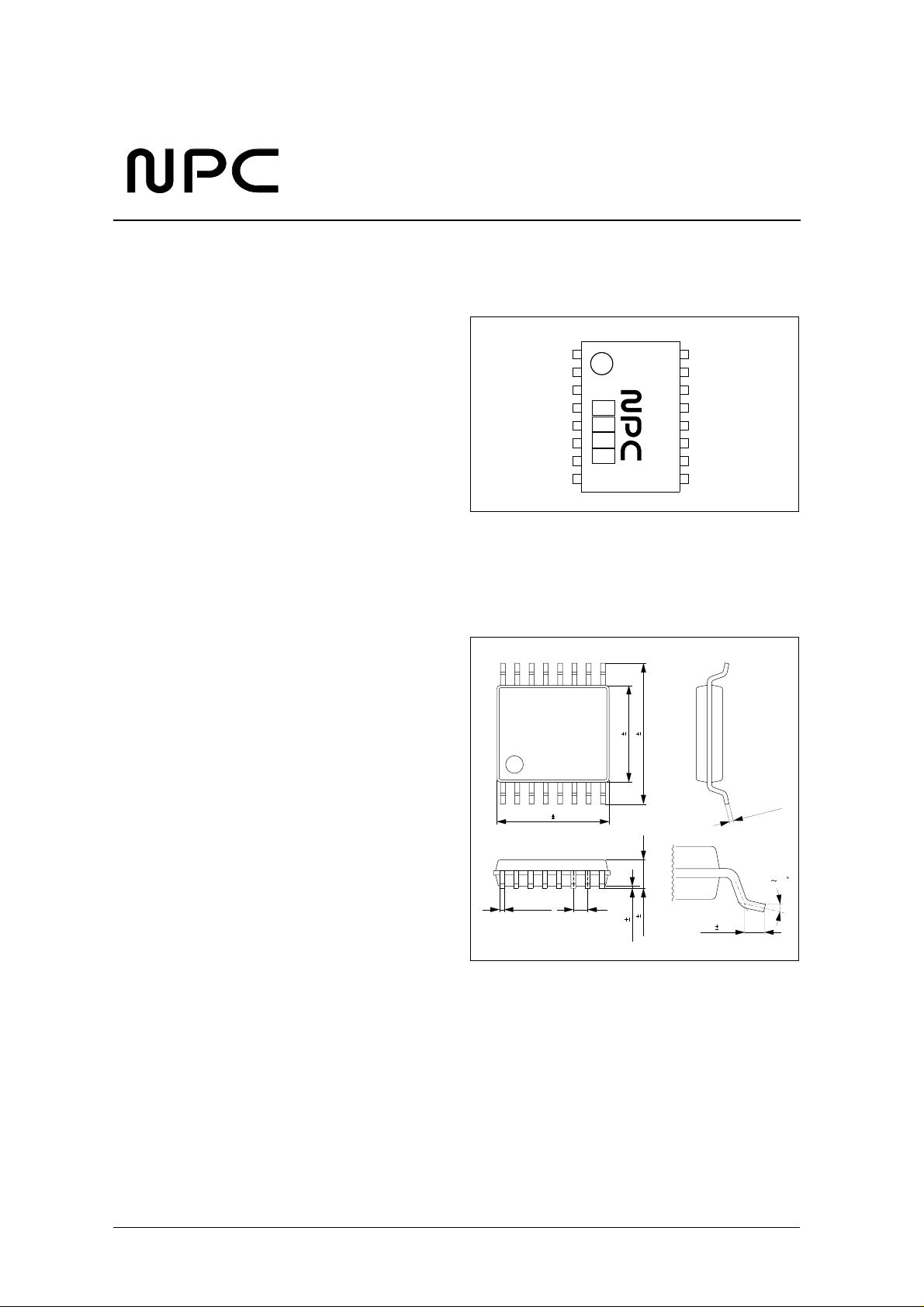
■
16-pin VSOP
■
Molybdenum-gate CMOS process
DD1
= 0.95 V)
DD1
= 1.00 V)
PLL Synthesizer IC
PINOUT
PACKAGE DIMENSIONS
Unit: mm
16-pin VSOP
(TOP VIEW)
XIN
XOUT
VDD2
DB
DO
VSS
FIN
VDD1
5.1 0.2
+ 0.10
0.22
- 0.05
1
16
5166
AV
8
4.4 0.2
6.4 0.2
0.65
1.15 0.1
0.10 0.05
TEST
NC
OPR
LE
DATA
CLK
LD
9
NC
+ 0.10
- 0.05
0.15
010
0.5 0.2
NIPPON PRECISION CIRCUITS—1
Page 2
BLOCK DIAGRAM
SM5166AV
XIN
XOUT
VDD2
VDD2
AREA
DATA
CLK
LATCH
SELECTOR
LE
OPR
VDD1
FIN
PIN DESCRIPTION
1/8
PRESCALER
VDD1
AREA
13 BIT
R COUNTER
14 BIT LATCH
16 BIT
SHIFT REGISTER
16 BIT LATCH
16 BIT
N COUNTER
LEVEL
SHIFTER
PHASE
DETECTOR
LEVEL
SHIFTER
GENERATOR
VDD1
AREA
SHIFTER
WINDOW
LEVEL
LOCK
DETECTOR
BOOSTER
S. G.
CHARGE
PUMP
TEST
LD
DB
DO
VSS
Number Name I/O Description
1 XIN I Reference frequency divider crystal (oscillator) connection pins. Alternatively, an external clock input can
2 XOUT O
3 VDD2 – Phase detector, charge pump and boost-up signal 3 V supply
4 DB O boost-up signal output for faster locking
5DOO
6 VSS – Ground pin
7 FIN I
8 VDD1 – Reference frequency and operating frequency prescaler and counter 1 V supply
9 NC – No connection
10 L D O
11 CLK I Control data clock input pin
12 DATA I Control data input pin
13 LE I Control data latch enable signal input pin
14 OPR I
15 NC – No connection
16 TEST I
be connected to XIN. The clock is also output on XOUT.
Feedback resistor b uilt-in f or AC-coupled inputs.
Phase detector output pin.
Built-in charge pump and tristate output means that this output can be connected to a low-pass filter.
The output polarity is preset for connection to a passive filter.
Operating frequency divider input pin.
Feedback resistor b uilt-in f or AC-coupled inputs.
Unlock signal output pin. (Unlocked when HIGH)
The function of LD can be turned OFF using the LD input control bit (LD should be tied LOW when not
used).
Power-save control pin.
Start when HIGH, standby mode when LOW.
Test pin.
Pull-down resistor built-in. Leave open or connect to ground for normal operation.
NIPPON PRECISION CIRCUITS—2
Page 3
SPECIFICATIONS
Absolute Maximum Ratings
V
= 0 V
SS
Parameter Symbol Pin name Rating Unit
Supply voltage
Input voltage range
Storage temperature range T
Power dissipation P
Soldering temperature T
Soldering time t
−
−
−
−
−
°
°
−
° C
SM5166AV
V
DD1
V
DD2
V
IN1
V
IN2
stg
D
sld
sld
VDD1
VDD2
FIN, XIN, TEST V
OPR, CLK, DATA, LE V
0.3 to 2.0 V
0.3 to 7.0 V
SS
SS
0.3 to V
0.3 to V
+ 0.3 V
DD1
+ 0.3 V
DD2
40 to 125
150 mW
255
10 s
C
C
Recommended Operating Conditions
V
= 0 V
SS
Parameter Symbol Condition Rating Unit
V
Supply voltage
Operating temperature range T
DD1
V
DD2
opr
Electrical Characteristics
V
= 0 V, V
SS
VDD1 operating current consumption I
VDD2 standby current I
FIN maximum operating input frequency f
XIN maximum operating input frequency f
FIN minimum operating input frequency f
XIN minimum operating input frequency f
FIN input amplitude V
XIN input amplitude V
OPR, CLK, DATA, LE LOW-level input
voltage
= 0.95 to 1.5 V, V
DD1
= 2.0 to 3.3 V, T
DD2
Parameter Symbol Condition
Note 1. – 0.70 1.10
DD1
DD2
max1
max2
min1
min2
V
Note 2. – 0.75 1.20
Note 3. – 0.01 10.0 µA
300 mVp-p sine
wave
300 mVp-p sine wave (external input) 25 – – MHz
300 mVp-p sine wave – – 40 MHz
300 mVp-p sine wave (external input) – – 9 MHz
V
DD1
AC coupling
FIN
V
DD1
AC coupling
f
= 25 MHz sine wave, AC coupling
XIN
XIN
(external input)
IL
= − 10 to 60 ° C
a
= 0.95 to 1.50 V, f
= 1.00 to 1.50 V, f
= 0.95 to 1.50
V
DD1
V
= 1.00 to 1.50
V
DD1
V
= 90 MHz,
FIN
= 100 MHz,
FIN
0.95 to 1.5 V
2.0 to 3.3 V
10 to 60
Rating
Unit
min typ max
mA
90 – –
MHz
100 – –
0.3 – –
Vp-p
0.3 – –
0.3 – – Vp-p
– – 0.3 V
NIPPON PRECISION CIRCUITS—3
Page 4
SM5166AV
−
Parameter Symbol Condition
OPR, CLK, DATA, LE HIGH-level input
voltage
FIN LOW-level input current I
XIN LOW-level input current I
FIN HIGH-level input current I
XIN HIGH-level input current I
DO , DB LOW-level output current I
DO, DB HIGH-level output current I
Tristate output high-impedance leakage
current
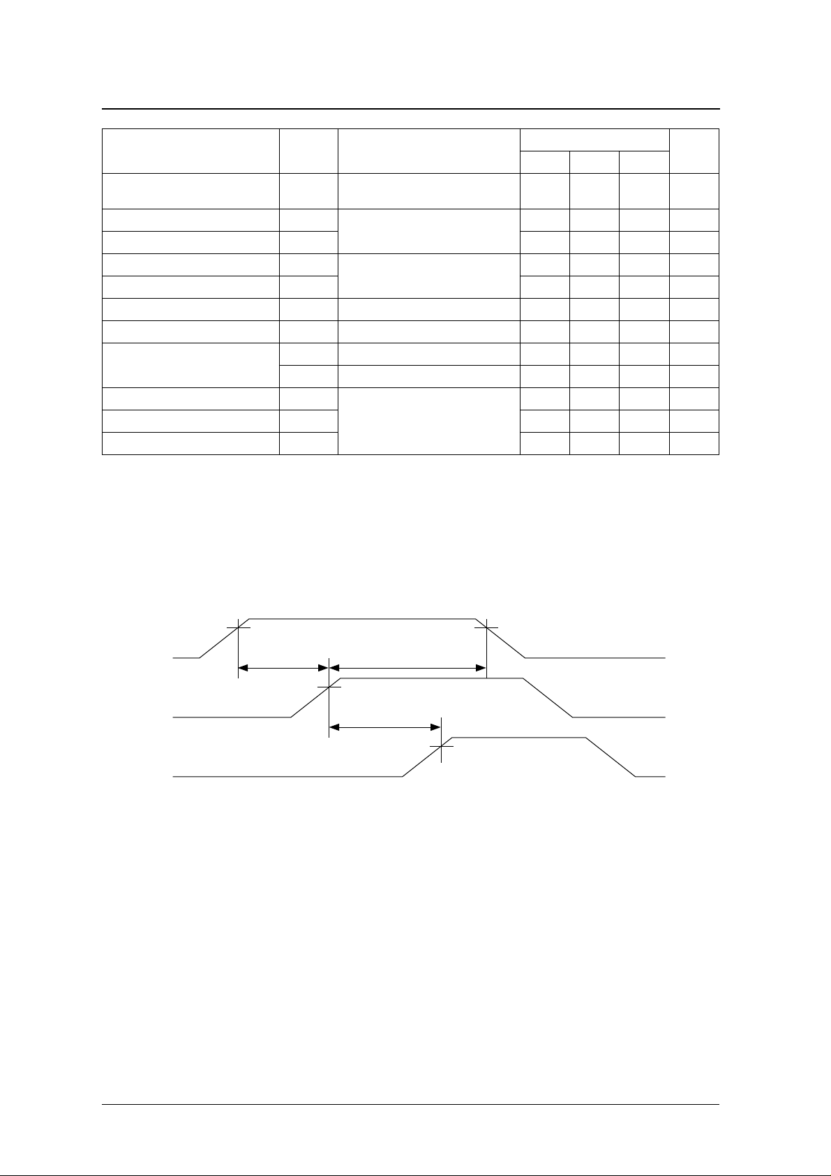
DATA → CLK setup time t
CLK → LE setup time t
Hold time t
1. V
= 0.95 to 1.05 V, V
DD1
load
2. V
= 1.00 to 1.05 V, V
DD1
load
3. V
= 0 V , V
DD1
4. DO and DB outputs are derived from the V
= 2.7 to 3.3 V , OPR = LOW, no input/output load (i.e. CLK = DATA = LE = 0 V)
DD2
= 2.7 to 3.3 V, f
DD2
= 2.7 to 3.3 V, f
DD2
5. DO and DB outputs are derived from the V
V
IH
IL1
V
= 0 V
IL2
IH1
IH2
OL
OH
I
OZL
I
OZH
SU1
SU2
H
= 90 MHz (300 mVp-p sine wave), f
FIN
= 100 MHz (300 mVp-p sine wave), f
FIN
supply. V
DD2
supply. V
DD2
IL
V
= V
IH
DD1
Note 4. 1.0 – – mA
Note 5. 1.0 – – mA
V
= 0 V – – 100 nA
OL
V
= V
OH
DD2
See the timing diagrams.
= 2.7 to 3.3 V , V
DD2
= 2.7 to 3.3 V , V
DD2
OL
OH
Rating
min typ max
1.5 – – V
––60µA
––10µA
––60µA
––10µA
– – 100 nA
2––µs
2––µs
2––µs
= 14.4 MHz (300 mVp-p sine wave), OPR = HIGH, no output
XIN
= 14.4 MHz (300 mVp-p sine wave), OPR = HIGH, no output
XIN
= 0.4 V
= V
0.4V
DD2
Unit
DATA, CLK, and LE timing
VIH
DATA
CLK
LE
tSU1
VIH
tH
VIH
tSU2
VIH
NIPPON PRECISION CIRCUITS—4
Page 5

SM5166AV
FUNCTIONAL DESCRIPTION
Operating Frequency Divider
(N-counter) Structure
The operating frequency divider generates a
comparator frequency signal (FV), which is input to
the phase comparator, by dividing the VCO signal
input on pin FIN.
The operating frequency divider is comprised by
dual modulus prescalers, a 5-bit swallow counter and
a 11-bit main counter.
The settings for the prescaler (P and P + 1), swallow
counter (S) and main counter (M) are related to the
comparator frequency divider ratio by:
NP1+()SPMS–()+×=
PM S+=
The counter value ranges are P = 32, P + 1 = 33, S =
0 to 31, and M = 32 to 2047. Therefore, the operating
frequency divider ratio range N is 1056 to 65535.
Reference Frequency Divider
(R-counter) Structure
Input Data
The input data should be specified keeping in mind
the V
DATA and LE pins into the shift register and latch
which operate from the V
V
DD1
The control data input uses a 3-line 17-bit serial
interface comprising the clock (CLK), data input
(DATA) and latch enable (LE). The data is input with
the MSB first. The last (17th) bit is used as the latch
select control bit. Data is written to the shift register
on the rising edge of the clock signal. Accordingly,
the data should change state on the falling edge of
the clock signal. Data is transferred from the shift
register to the latch when the latch enable (LE)
signal goes HIGH. Accordingly, the latch enable
signal should be held LOW while data is being
written to the shift register.
The clock and data input signals are both ignored
when the latch enable signal goes HIGH. Also, the
CLK, DATA and LE inputs should be tied LOW
when not setting data.
supply. The data is input using CLK,
DD2
supply. However, the
DD2
supply level can vary.
The reference frequency divider generates a
comparator frequency signal (FR), which is input to
the phase comparator, by dividing the reference
frequency input either from an external signal on
XIN or from a crystal connected between XIN and
XOUT.
The reference frequency divider is comprised by a
fixed divide-by-8 prescaler and an 13-bit reference
counter.
The settings for the prescaler (A = 8) and reference
counter (R) are related to the reference frequency
divider ratio by:
RAB8B==
The counter value ranges are A = 8 and B = 5 to
8191. Therefore, the reference frequency divider
ratio range is R = 40 to 65528.
NIPPON PRECISION CIRCUITS—5
Page 6

Input Data Format
Shift register timing
CLK
1234567891011121314151617
SM5166AV
) ×
DATA
MSB LSB
CONTROL
LE
Figure 1. Comparator data format
Latch select
The last (17th) data bit determines the status of the
shift register data latch.
Table 1. Latch select bit function
Bit 17 Latch
Swallow counter and main counter frequency divider
0
ratio latch select
Reference frequency counter divider ratio data and
1
LD output latch select
Swallow counter and main counter frequency divider
MSB LSB
DATA 1234567891011121314151617
10987654321043210
2222222222222222
Main counter
(11-bit : 32 to 2047)
Figure 2. Swallow counter and main counter frequency divider data format
Input data example
If the VCO output (f
frequency (f
bandwidth (f
) is 251.3 MHz, and the channel
LO
: operating frequency (f
CH
) is trebled, the output
VCO
R
3) is 25
kHz, then the comparator frequency divider ratio N
is given by:
f
N
--------- f
LO
CH
f
VCO
----------------------fR3×
3×
251.3 3⁄
-------------------- 10052 32 314 4+×== = = =
0.025 3⁄
Therefore, the swallow counter count is 4 (00100)
and the main frequency divider counter count is 314
(0000100111010)
. The input data format is shown
2
in figure 3.
Swallow counter
(5-bit : 0 to 31)
Latch selection bit : Set to "0"
2
NIPPON PRECISION CIRCUITS—6
Page 7

SM5166AV
MSB LSB
1234567891011121314151617
10987654321043210
2222222222222222
Input
00100111010001000
Data
Main counter
(11-bit : 32 to 2047)
Swallow counter
(5-bit : 0 to 31)
Latch selection bit : Set to "0"
Figure 3. Swallow counter and main counter frequency divider data example
Reference counter frequency divider setting
MSB LSB
DATA 1234567891011121314151617
1211109876543210
2222222222222
(Reference counter 13-bit : 5 to 8191)
LD output setting bit
∗
Test bits : (15, 16) = (0, 0) for normal operation
: Normal operation when 1,
Latch selection bit : Set to "1"
∗
LOW-level output when 0.
Figure 4. Reference counter data and LD output setting format
Input data example
If the VCO output (f
) is trebled, the crystal
VCO
frequency is 12.8 MHz and the channel bandwidth
(fCH: comparator frequency (fR) × 3) is 25 kHz, then
the reference frequency divider ratio R is given by:
NR
Xtal
---------- f
CH
Xtal
--------------fR3×
12.8
-------------------- 1536 8 192×== = ==
0.025 3⁄
Therefore, the reference counter count is 192
(00011000000)2. The input data format is shown in
figure 5.
NIPPON PRECISION CIRCUITS—7
Page 8

SM5166AV
MSB LSB
1234567891011121314151617
1211109876543210
2222222222222
Input
Data
00000110000001001
(Reference counter 13-bit : 5 to 8191)
LD output setting bit
∗
Test bits : (15, 16) = (0, 0) for normal operation
Latch selection bit : Set to "1"
Figure 5. Reference counter data and LD output setting example
NIPPON PRECISION CIRCUITS—8
Page 9

SM5166AV
Boost-up Signal
If the PLL momentarily loses lock as a result of a
phase error, a level signal is output on pin DB. When
the PLL is operating in lock, output DB goes high
impedance.
When the PLL starts up, the signal on DB charges
the low-pass filter capacitor in anticipation of highspeed locking. After the boost-up signal is output and
the PLL phase error comes within tolerance, the
boost-up circuit stops and operation continues when
, V
the 2 supplies (V
DD1
goes HIGH once only. After the boost-up circuit
stops, new data is written and the boost-up signal is
not output even if the VCO is not in lock.
FR
FV
) are applied and OPR
DD2
Operating principles
When the PLL is operating with a phase error within
fixed tolerance, an internal WINDOWN signal is
generated, as shown in figure 6. This signal is in sync
with the N counter output signal (FV) and is 64
cycles of the FIN input period in length centered
about the falling edge of FV.
If the phase detector error correction signal occurs
before the WINDOWN LOW-level pulsewidth, the
HIGH-level output from DB continues. However, if
the error correction signal occurs wholly within the
WINDOWN LOW-level pulsewidth, DB goes high
impedance and the boost-up circuit operation stops.
The above description applies when the error
correction signal is revising up. When the error
correction signal is revising down, DB goes LOW.
Phase Detector
error correction signal
WINDOWN
DB
Hi-Impedance Hi-Impedance
Figure 6. boost-up signal timing
Standby Mode
The SM5166AV enters standby mode when OPR
goes LOW. In this mode, the states and functions
shown in table 2 occur.
In standby mode, some current flows into VDD1
(FIN and XIN prescaler current). Therefore, it is
necessary to reduce V
to 0 V to fully reduce
DD1
∗∗ ∗∗
HIGH level output
: 32fFIN
()
∗
current consumption and reduce power dissipation.
Table 2. Standby mode block states
Block State
DO and DB Floating (high impedance)
LD LOW-level output
Phase
comparator
Input FIN Feedback resistor is cutoff (HIGH le vel )
Input XIN Feedback resistor is cutoff (HIGH level)
Reset
N counter Reset
R counter Reset
Latch data Stored (while V
NIPPON PRECISION CIRCUITS—9
is within rating)
DD2
Page 10

SM5166AV
Phase Comparator Timing Diagram
The DO output circuit polarity is configured for
connection to an external passive filter.
The signals compared are FV and FR, which are the
internal operating frequency divider output signal
and reference frequency divider output signal,
respectively.
The timing and passive filter basic structure are
shown in figures 7 and 8, respectively.
FR
FV
DO
LD
Figure 7. Phase detector timing
R1
DO
VCO
R2
C
Figure 8. Passive filter
NIPPON PRECISION CIRCUITS INC. reserves the right to make changes to the products described in this data sheet in order to
improve the design or performance and to supply the best possible products. Nippon Precision Circuits Inc. assumes no responsibility for
the use of any circuits shown in this data sheet, conveys no license under any patent or other rights, and makes no claim that the circuits
are free from patent infringement. Applications for any devices shown in this data sheet are for illustration only and Nippon Precision
Circuits Inc. makes no claim or warr anty that such applications will be suitab le for the use specified without further testing or modification.
The products described in this data sheet are not intended to use for the apparatus which influence human lives due to the failure or
malfunction of the products. Customers are requested to comply with applicable laws and regulations in effect now and hereinafter,
including compliance with export controls on the distribution or dissemination of the products. Customers shall not expor t, directly or
indirectly, any products without first obtaining required licenses and approvals from appropriate government agencies.
NIPPON PRECISION CIRCUITS INC.
NIPPON PRECISION CIRCUITS INC.
4-3, 2-chome Fukuzumi
Koutou-ku, Tokyo 135-8430, Japan
Telephone: 03-3642-6661
Facsimile: 03-3642-6698
NC9610BE 1997.05
NIPPON PRECISION CIRCUITS—10
Page 11

SM5166AV
INPUT/OUTPUT EQUIVALENT CIRCUITS
XIN, XOUT DO
VDD2
XOUT
From
Internal
Circuit
XIN
VDD1
VDD1
To
Internal
Counter
LD
Internal
Circuit
From
Internal
Circuit
VDD1
Transistor
Resistor
FIN DB
VDD1
From
Internal
Circuit
FIN1
VDD1
To
Internal
Counter
Diffused Resistor
Lagging Phase
Correction Signal
Leading Phase
Correction Signal
From
Internal
Circuit
From
Internal
Circuit
From
Internal
Circuit
DO
VDD2
LD
VDD2
DB
OPR, CLK, DATA, LE TEST
VDD1
To
Internal
Circuit
OPR
CLK
DATA
LE
VDD2
To
Internal
Circuit
VDD1
TEST
Transistor Resistor
NIPPON PRECISION CIRCUITS INC. reserves the right to make changes to the products described in this data sheet in order to
improve the design or performance and to supply the best possible products. Nippon Precision Circuits Inc. assumes no responsibility for
the use of any circuits shown in this data sheet, conveys no license under any patent or other rights, and makes no claim that the circuits
are free from patent infringement. Applications for any devices shown in this data sheet are for illustration only and Nippon Precision
Circuits Inc. makes no claim or warr anty that such applications will be suitab le for the use specified without further testing or modification.
The products described in this data sheet are not intended to use for the apparatus which influence human lives due to the failure or
malfunction of the products. Customers are requested to comply with applicable laws and regulations in effect now and hereinafter,
including compliance with export controls on the distribution or dissemination of the products. Customers shall not expor t, directly or
indirectly, any products without first obtaining required licenses and approvals from appropriate government agencies.
NIPPON PRECISION CIRCUITS INC.
4-3, 2-chome Fukuzumi
Koutou-ku, Tokyo 135-8430, Japan
NIPPON PRECISION CIRCUITS INC.
Telephone: 03-3642-6661
Facsimile: 03-3642-6698
NC9610BE 1997.05
NIPPON PRECISION CIRCUITS—11
 Loading...