

Page 1
NIPPON PRECISION CIRCUITS INC.
NIPPON PRECISION CIRCUITS-1
SM5160CM/DM
Programable PLL Frequency Synthesizer
60
XIN
XOUT
VDD3
DOA
DOP
VSS
FIN
TEST
FR
FV
LE
DATA
CLK
LD
VDD1 VDD2
1
89
16
1
OVERVIEW
The SM5160CM/DM is a PLL frequency synthesizer
IC with programmable input and reference frequency
dividers.
The SM5160CM/DM features an unlock detector, outputs for use with active passive lowpass filters and direct
frequency divider outputs.
The SM5160CM/DM operates from 0.95 to 2.00 V
and 2.0 to 3.3 V supplies and is available in 16-pin
SSOPs.
FEATURES
• Up to 95 MHz input frequency (FIN, VDD= 0.98V)
• Up to 90 MHz input frequency (FIN, VDD= 0.95V)
• Up to 13.0 MHz reference frequency (XIN)
• 1056 to 65535 programmable input frequency
divider ratio
• 20 to 65532 programmable reference frequency
divider ratio (SM5160CM)
• 20 to 8188 programmable reference frequency
divider ratio (SM5160DM)
• Unlock detector
• Outputs for use with active and passive lowpass
filters
• Direct outputs from frequency dividers
• 0.95 to 2.0 V and 2.0 to 3.3 V supplies
• Molybdenum- gate CMOS process
• 16-pin SSOP
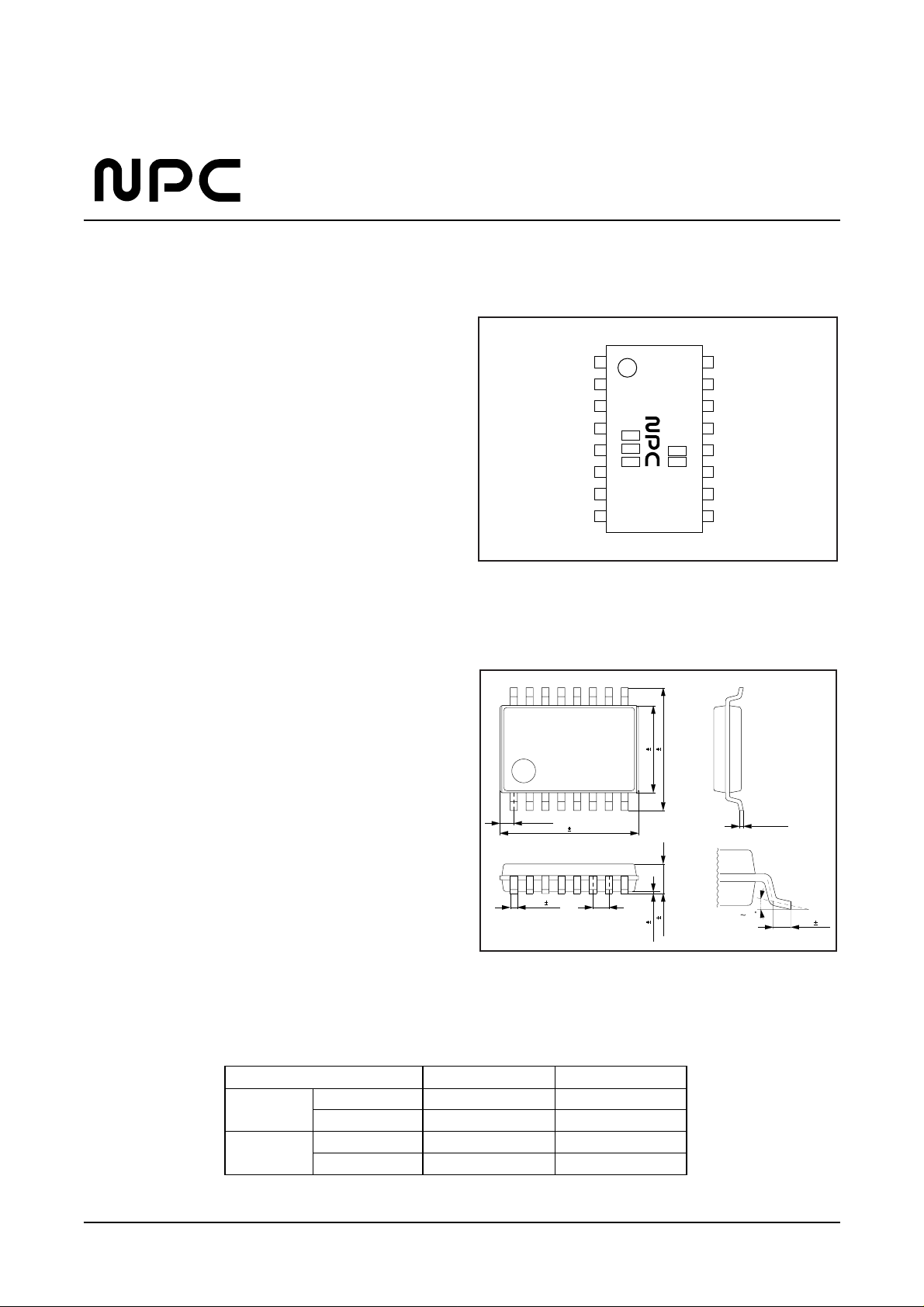
PACKAGE DIMENSIONS
(Unit: mm)
SERIES LINEUP
XIN FIN
SM5160CM Divider range 20 to 65532 (4 step) 1056 to 65535
Counter bits 14 bit 16 bit
SM5160DM Divider range 20 to 8188 (4 step) 1056 to 65535
Counter bits 11 bit 16 bit
PINOUT
(Top View)
4.4 0.2
6.2 0.3
0.6TYP
6.8 0.3
0.80.36 0.1
1.5 0.1
0.05 0.05
+ 0.10
0.15
- 0.05
010
0.4 0.2
Page 2
NIPPON PRECISION CIRCUITS-2
SM5160CM/DM
BLOCK DIAGRAM
11 or 14 BIT
R COUNTER
PHASE
DETECTOR
LOCK
DETECTOR
CHARGE
PUMP
16 BIT N COUNTER
FIN
DATA
LD
FV
XOUT
LE
CLK
FR
DOA
DOP
16 BIT LATCH
14 BIT LATCH
17 BIT SHIFT REGISTER
XIN
1/4
PRESCALER
LEVEL
SHIFTER
LEVEL
SHIFTER
VDD1
VDD2
VDD3
VDD1
VDD2
TEST
PIN DESCRIPTION
Number Name Description
1 XIN Reference oscillator or external clock input. Internal feedback resistor for AC coupling
2 XOUT Reference oscillator or external clock output. Oscillator is OFF when VDD1 is LOW.
3 VDD3 Supply voltage for sections not supplied by VDD1 and VDD2
4 DOA Output to active lowpass filter. Single-ended, tristate output. Floating when VDD1 is LOW
5 DOP Output to passive lowpass filter. Single-ended, tristate output Floating when VDD1 is LOW
6 VSS Ground
7 FIN Comparison frequency input. Internal feedback resistor for AC coupling
8 VDD1 Supply voltage for XIN and FIN amplifiers
9 VDD2 Supply voltage for N counter and R counter
10 LD Unlock detector output. LOW when PLL is unlocked.
11 CLK Shift register clock input
12 DATA Serial data input
13 LE Latch enable input
14 FV Input frequency divider buffered output. This is level-shifted and input to the phase detector.
15 FR Reference frequency divider buffered output. This is level-shifted and input to the phase detector.
16 TEST Test input. Internal pull-down resistor
Page 3
NIPPON PRECISION CIRCUITS-3
SM5160CM/DM
SPECIFICATIONS
Absolute Maximum Ratings
Electrical Characteristics
Parameter Symbol Condition Rating Unit
Supply voltage range 1 V
DD1−VSS −0.3 to +7.0 V
V
DD2−VSS
Supply voltage range 2 VDD3-VSS −0.3 to +7.0 V
Input voltage range V
IN VSS−0.3 to VDD+0.3 V
Operating temperature range T
OPR −10 to +60 °C
Storage temperature range T
STG −40 to +125 °C
Soldering temperature range T
SLD 250 °C
Soldering time range
tSLD 10 sec
Rating
Parameter Symbol Condition min typ max Unit
Supply voltage 1 V
DD1,VDD2 VDD1 and VDD2 pins 0.95 1.00 2.0 V
Supply voltage 2 V
DD3 VDD3 pin 2.0 3.0 3.3 V
F
IN= 90MHz, 0.5VP-P sine wave
X
IN= 12.8MHz, 0.5VP-P sine wave 0.80 1.20 mA
Current consumption I
DD1 VDD1= VDD2= 0.95 to 1.05V
(*1) F
IN= 95MHz, 0.5VP-P sine wave
X
IN= 12.8MHz, 0.5VP-P sine wave 0.85 1.40 mA
V
DD1= VDD2= 0.98 to 1.08V
Standby-mode current consumption I
DD2 VDD1= VDD2= 0V 10 µA
F
IN: 0.5VP-P sine wave 90 MHz
FIN maximum operating frequency f
MAX1 VDD1= VDD2= 0.95 to 2.0V
F
IN: 0.5VP-P sine wave 95 MHz
V
DD1= VDD2= 0.98 to 2.0V
XIN maximum operating frequency f
MAX2 XIN: 0.5VP-P sine wave 13 MHz
FIN minimum operating frequency f
MIN1 FIN: 0.5VP-P sine wave 40 MHz
XIN minimum operating frequency f
MIN2 XIN: 0.5VP-P sine wave 7 MHz
FIN and XIN input voltage V
IN FIN and XIN pins 0.5 VDD1 VP-P
CLK, DATA and LE VIH VDD3− 0.3 V
input voltage V
IL 0.3 V
XIN input current I
IH1 VIH= VDD1 10 µA
I
IL1 VIL= 0V 10 µA
FIN input current I
IH2 VIH= VDD1 60 µA
I
IL2 VIL= 0V 60 µA
DOA and DOP I
OH1 VDD3= 2.7 to 3.3V, VOH= VDD3− 0.4V 1.0 mA
output current I
OL1 VDD3= 2.7 to 3.3V, VOL= 0.4V 1.0 mA
LD, FV and FR I
OH1 VOH= VDD2− 0.4V 0.1 mA
output current I
OL1 VOH= 0.4V 0.1 mA
DATA to CLK and CLK to LE
tSU1 2 µs
setup time
tSU2 2 µs
hold time
tH 2 µs
(VDD1= VDD2= 0.95 to 2.0V, VDD3= 2.0 to 3.3V, VSS= 0V, Ta= −10 to +60 °C unless otherwise noted)
*1 Current consumption is the current consumed from V
DD1 and VDD2.
Page 4

NIPPON PRECISION CIRCUITS-4
SM5160CM/DM
Serial data input timing
Phase detector timing
CLK
DATA
LE
50%
tSU1 tH
tSU2
50%
50%
50%
FR
FV
LD
DOA
DOP
Page 5

NIPPON PRECISION CIRCUITS-5
SM5160CM/DM
Lowpass Filter Connection
An external lowpass filter connects to DOP or DOA.
The output form the filter is fed to a voltage-controlled
oscillator (VCO) which generates the PLL output.
DOP is intended for use with a passive filter as shown
in figure 1. DOA is intended for use with an active filter
as shown in figure 2.
Figure 1. Passive lowpass filter circuit
Figure 2. Active lowpass filter circuit
Programmable Frequency Divider
The input frequency divider and reference frequency
divider ratios can be programmed using the serial data
input.
Input data consists of 16 data bits, in the order msb to
lsb, followed by a control bit, as shown in figure 3 and 4.
SM5160CM
If the control bit is set to 0, the data is written to the
16-bit latch and then passed to the input frequency
divider.
If the control bit is set to 1, the 2 lsbs are ignored and
the remaining data is written to the 14-bit latch and then
passed to the reference frequency divider.
Figure 3. Serial data format (SM5160CM)
SM5160DM
If the control bit is set to 0, the data is written to the
16-bit latch and then passed to the input frequency
divider.
If the control bit is set to 1, the 2 lsbs and 3msbs are
ignored and the remaining data is written to the 11-bit
latch and then passed to the reference frequency divider.
DOP
C
R2
R1
VCO
VDD
DOA
RL
R1
R2
V
DD
VCO
C
510kΩ
FUNCTIONAL DESCRIPTION
MSB
CONTROL
LSB
ignored
16BIT (N- COUNTER DATA)
14BIT (R- COUNTER DATA)
1: R-LATCH 0: N-LATCH
MSB
CONTROL
LSB
ignored ignored
16BIT (N- COUNTER DATA)
11BIT (R- COUNTER DATA)
1: R-LATCH 0: N-LATCH
Figure 4. Serial data format (SM5160DM)
Page 6

NIPPON PRECISION CIRCUITS-6
SM5160CM/DM
Serial data input timing
Serial data input timing is shown in figure 5. Data is
read on the rising edge of CLK. The state on DATA
should be changed in sync with the falling edge of CLK.
LE should be LOW while data is being written to the
shift register. When LE goes HIGH, data is transferred
from the shift register to one of the frequency divider
latches.
Stand-by mode
The stand-by mode is entered by setting VDD1,
VDD2 to 0V while the device is operation.
In the stand-by mode, the amplifiers of XIN, FIN and
N/R counter are stopped. As long as voltage is provide to
VDD3, data written in latch is kept. Exit from this mode
to normal operation, therefore, is made by providing voltage to VDD1, VDD2. In this mode, input to FIN must
be done AC coupling, input to XIN must be done AC
coupling or by crystal oscillator. In this mode, DOA,
DOP should be in state of floating.
CLK
DATA
1234567891011121314151617
LE
MSB
CONTROL
LSB
Figure 5. Serial data input
Page 7

NIPPON PRECISION CIRCUITS-7
SM5160CM/DM
NC9506AE 1995 8
NIPPON PRECISION CIRCUITS INC.
TYPICAL APPLICATION
(For Ex. : in case of Pager)
NIPPON PRECISION CIRCUITS INC. reserves the right to make changes to the products described in this data sheet in order to
improve the design or performance and to supply the best possible products. Nippon Precision Circuits Inc. assumes no responsibility for
the use of any circuits shown in this data sheet, conveys no license under any patent or other rights, and makes no claim that the circuits
are free from patent infringement. Applications for any devices shown in this data sheet are for illustration only and Nippon Precision
Circuits Inc. makes no claim or warranty that such applications will be suitable for the use specified without further testing or modification. The products described in this data sheet are not intended to use for the apparatus which influence human lives due to the failure or
malfunction of the products. Customers are requested to comply with applicable laws and regulations in effect now and hereinafter, including compliance with export controls on the distribution or dissemination of the products. Customers shall not export, directly or indirectly, any products without first obtaining required licenses and approvals from appropriate government agencies.
NIPPON PRECISION CIRCUITS INC.
4-3, 2-chome Fukuzumi, Koto-ku
Tokyo, 135 -8430, JAPAN
Telephon: 03-3642-6661
Facsimile: 03-3642-6698
DC/ DC
CONVERTER
XIN
XOUT
VDD3
DOA
DOP
VSS
FIN
TEST
FR
FV
LE
DATA
CLK
LD
VDD1 VDD2
LCD
DRIVER
DRIVER
RAM ROM
CPU DECODER
Display
LPF
B++
B+
SM5160
WAVE
SHAPER
DISCB+
2'nd
IF
1'st
IF
1'st
MIX
RF
AMP
2'nd
MIX
1'st
LO
2'nd
LO
Frequency
Multiplier
3
 Loading...