

Page 1
DISCONTINUED
PRODUCT
SM5128A1
NIPPON PRECISION CIRCUITS INC.
OVERVIEW
The SM5128A1 is a CB transceiver system CMOS
IC that incorporates a PLL synthesizer, USA-frequency specification code ROM, channel up/down
control circuit, LCD driver and channel-change
unlock signal generator. All these features in a single
chip allow the overall system cost to be reduced.
FEATURES
USA-specification code ROM
■
Channel up/down control circuit
■
Unlock signal generator circuit
■
Channel/PA display decoder
■
LCD driver
■
Channel-change confirmation tone output signal
■
Amplifier for an active low-pass filter
■
Single-crystal PLL synthesizer
■
4.5 to 5.5 V supply voltage
■
10.24 MHz crystal oscillator circuit
■
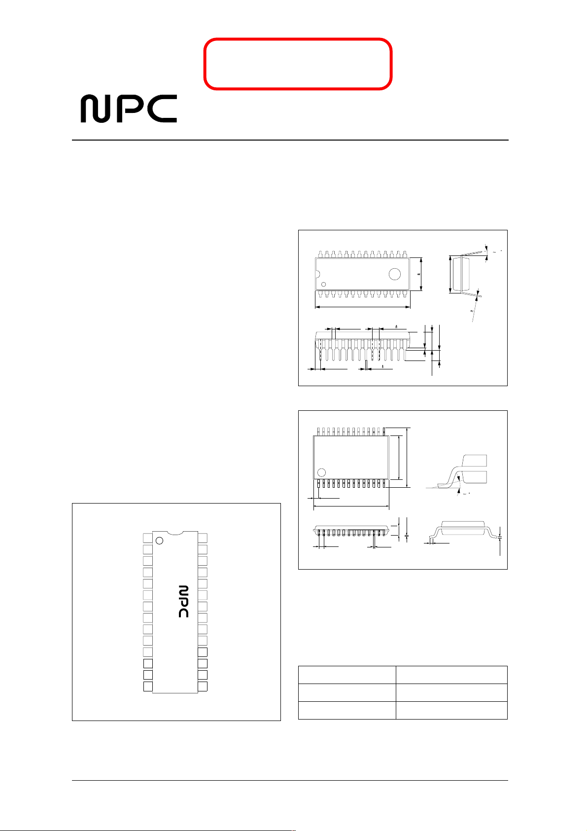
28-pin shrink DIP (SM5128A1N)
■
28-pin VSOP(SM5128A1V)
■
Molybdenum-gate CMOS process
■
PINOUT
Top View
1COMC
2S1
3S2
4S3
SM5128A1
5S4
6S5
7S6
8HL
9LB
10PA
11TEST
12XOUT
13XIN
14VSS 15 FIN
28 COMB
27 COMA
26 UP
25 DN
24 EMG
23 TR
22 CE
21 CHO
20 LD
19 AO
18 AI
17 DO
16 VDD
CB Transceiver System LSI
PACKAGE DIMENSIONS
Unit: mm
28-pin Shrink DIP
9.10 0.25
+ 0.20
26.00
− 0.30
+ 0.50
1.00
− 0
1.778MAX
28-pin VSOP
0.675 TYP
+
9.8 0.2
-
0.65
ORDERING INFOMATION
Device Package
SM5128A1N 28pin SDIP
1.778 0.18
0.45 0.10
+
-
0.22
0.1
0.05
0.51MIN
4.85MAX
0.2
0.2
-
-
+
+
5.6
7.6
-
+
-
+
1.15 0.1
0.10 0.05
3.00MIN
+
0.5 0.2
-
10.16TYP
0
0.25 0.05
10
015
0.1
+
0.05
-
0.15
SM5128A1V 28pin VSOP
NIPPON PRECISION CIRCUITS—1
Page 2
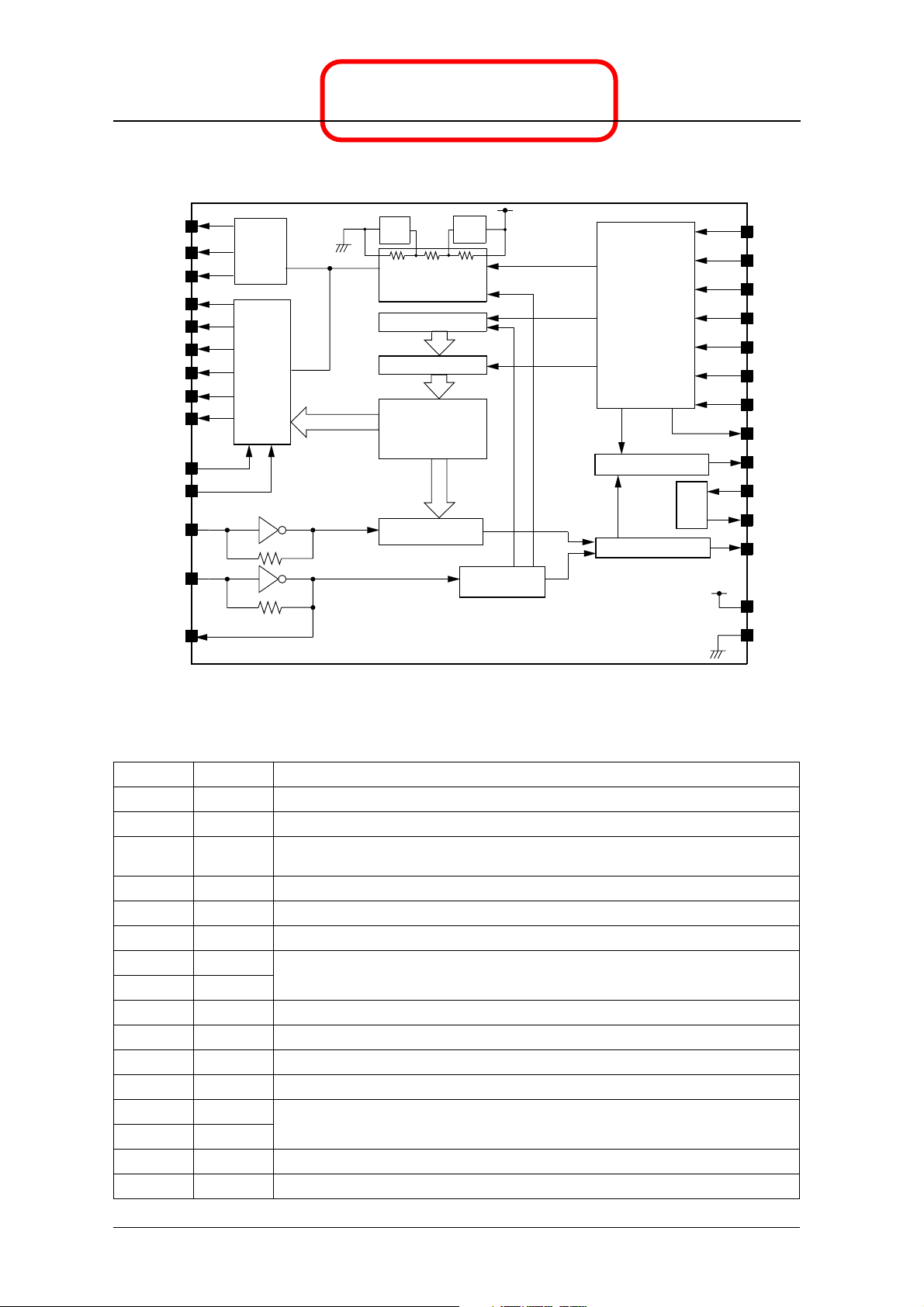
BLOCK DIAGRAM
COMA
COMB
COMC
S1
S2
S3
S4
S5
S6
LB
HL
FIN
XIN
LCD
COM
LCD
DRIVER
DISCONTINUED
SM5128A1
PRODUCT
SW2
LCD DRIVING
SIGNAL
GENERATOR
UP/DN COUNTER
MULTI PLEXER
CHANNEL ROM
PROGRAMMABLE
DIVIDER
SW1
REFERENCE
DIVIDER
CONTROLLER
LD CONTROLLER
AMP
PHASE DETECTOR
TEST
CE
PA
UP
DN
EMG
TR
CHO
LD
AI
AO
DO
VDD
XOUT
PIN DESCRIPTION
Number Name Description
1 COMC LCD common drive signal output
2 to 7 S1 to S6 LCD segment drive signal output
8HL
9LB“LOW BATTERY” display indicator input. “LOW BATTERY” indicator when LOW or open. Pull-down resistor built-in.
10 PA PA input. PA mode when HIGH. Pull-down resistor built-in.
11 TEST Test input. Tie LOW or open for normal operation.
12 XOUT
13 XIN
14 VSS Ground
15 FIN Programmable counter input. Feedback resistor built-in.
16 VDD 4.5 to 5.5 V supply voltage
17 DO Phase detector output. Three-state output pin.
18 AI
19 AO
20 LD Unlock signal output. Unlocked when LOW, and locked when HIGH.
21 CHO Channel-change confirmation tone output. Active-HIGH pulse of approximately 50 ms duration.
“HIGH POWER”/”LOW POWER” display indicator control input. “HIGH POWER” indicator when HIGH, and “LOW
POWER” indicator when LOW or open. Pull-down resistor built-in.
Crystal oscillator circuit input and output
Inverter input and output. AI is HIGH in standby mode.
VSS
NIPPON PRECISION CIRCUITS—2
Page 3
−
−
°
−
°
°
−
−
−
DISCONTINUED
SM5128A1
PRODUCT
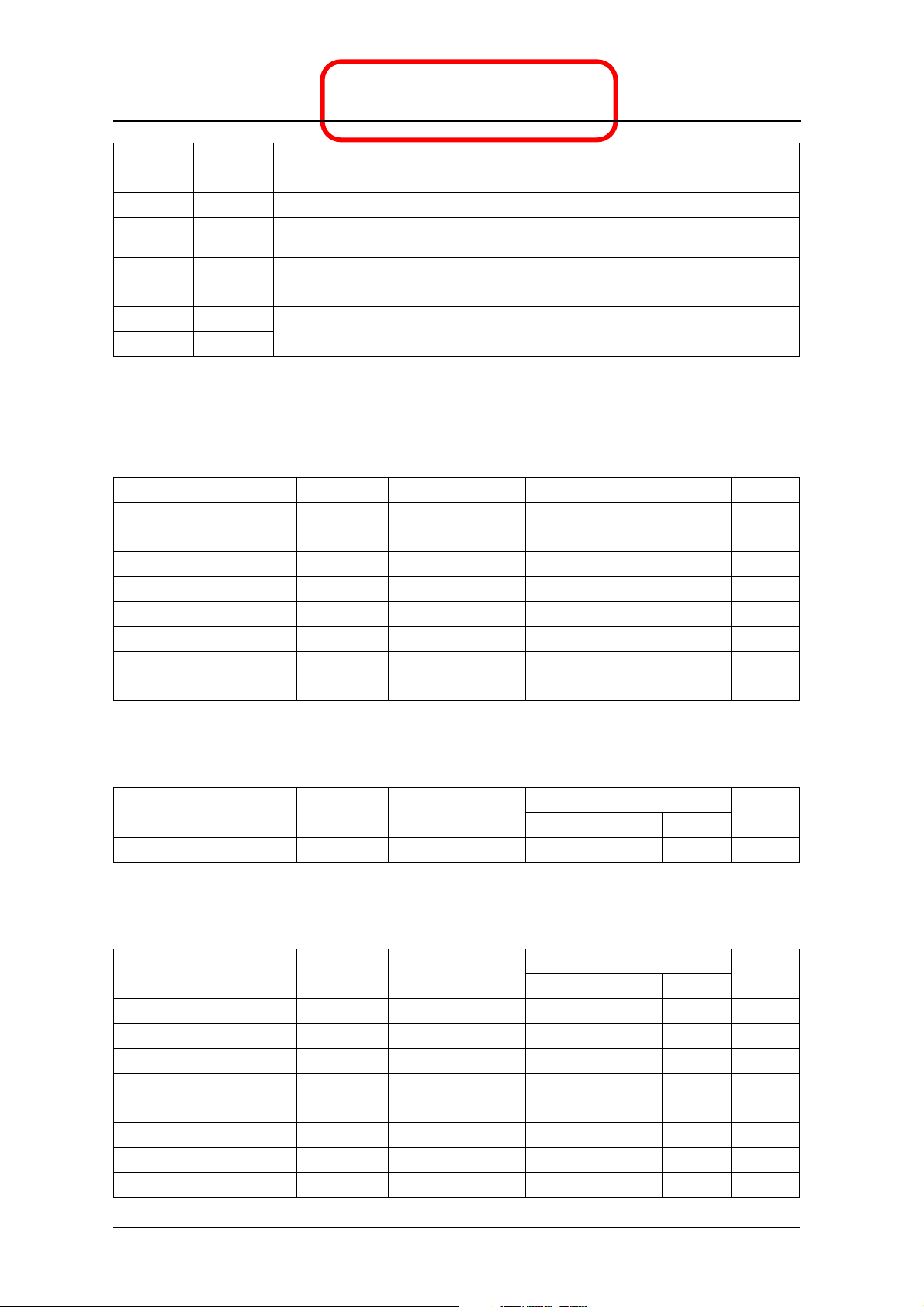
Number Name Description
22 CE PLL start pin. Start when HIGH, and standby mode when LOW. Pull-down resistor built-in.
23 TR Transmit/Receive switch input. Transmit when HIGH, and receive when LOW or open. Pull-down resistor built-in.
24 EMG
25 UP Channel-change up control input. Change up when HIGH. Pull-down resistor built-in.
26 DN Channel-change down control input. Change down when HIGH. Pull-down resistor built-in.
27 COMA
28 COMB
SPECIFICATIONS
Absolute Maximum Ratings
V
= 0 V
SS
Parameter Symbol Condition Rating Unit
Supply voltage V
Input voltage range V
Power dissipation P
Operating temperature T
Storage temperature range T
Soldering temperature T
Soldering time t
Output current I
Emergency channel select input. Channel 9 when HIGH, and the previously set channel with channel up/down
control when LOW or open. Pull-down resistor built-in.
LCD common drive signal outputs
DD
IN
D
opr
stg
sld
sld
O
0.3 to 7.0 V
V
to V
SS
DD
150 mW
30 to 80
40 to 125
255
10 s
10 mA
V
C
C
C
Recommended Operating Conditions
V
= 0 V
SS
Parameter Symbol Condition
Supply voltage V
DD
Electrical Characteristics
V
= 0 V, Ta=–30 to 80 ˚C, V
SS
Parameter Symbol Condition
Operating consumption current
1
FIN maximum operating frequency f
XIN maximum operating frequency f
FIN operating input voltage V
XIN operating input voltage V
LOW-level input voltage
HIGH-level input voltage
2
2
FIN and XIN start voltage V
=4.5 to 5.5V unless otherwise noted
DD
I
DD
max1
max2
IN1
IN2
V
IL1
V
IH1
IO
1.0 Vp-p sine wave 18 ––MHz
1.0 Vp-p sine wave 12 ––MHz
18 MHz sine wave 1.0 – V
10.24 MHz sine wave 1.0 – V
V
DD
Rating
min typ max
Unit
4.5 5.0 5.5 V
Rating
min typ max
Unit
––10 mA
1Vp-p
DD
1Vp-p
DD
––0.4 V
V
0.4 ––V
DD
= 5.0 V 2.0 2.5 3.0 V
NIPPON PRECISION CIRCUITS—3
Page 4
µ
µ
µ
µ
µ
µ
µ
−
−
−
−
−
DISCONTINUED
PRODUCT
Parameter Symbol Condition
FIN and XIN LOW-level input current I
FIN and XIN HIGH-level input current I
LOW-level input current
HIGH-level input current
2
2
AI LOW-level input current I
AI HIGH-level input current I
Standby current I
COMA, COMB, COMC LOW-level
output voltage
COMA, COMB, COMC HIGH-level
output voltage
S1 to S6 LOW-level output voltage V
S1 to S6 HIGH-level output voltage V
LD, CHO, DO LOW-level output
voltage
LD, CHO, DO HIGH-level output
voltage
AO LOW-level output voltage V
AO HIGH-level output voltage V
XOUT LOW-level output voltage V
XOUT HIGH-level output voltage V
DO, AI HIGH-level leakage current I
DO, AI LOW-level leakage current I
V
V
V
V
IL1
IH1
I
IL2
I
IH2
IL3
IH3
STB
OL1
OH1
OL2
OH2
OL3
OH3
OL4
OH4
OL5
OH5
LH
LL
1. FIN = 16.71 MHz and 1.0 Vp-p, XIN = 10.24 MHz and 1.0 Vp-p
2. Pins HL, LB, PA, TEST, CE, TR, EMG, DN, UP.
V
V
V
V
V
T
V
T
CE = open, T
I
OL
I
OH
I
OL
I
OH
I
OL
I
OH
I
OL
I
OH
I
OL
I
OH
V
T
V
T
SM5128A1
Rating
min typ max
= 0 V, V
IL1
= V
IH1
= 0 V, V
IL2
= V
IH2
= 0 V, V
IL3
= 25 ° C
a
= V
IH3
= 25 ° C
a
= 10 µ A ––0.4 V
= 10 µ AV
= 10 µ A ––0.4 V
= 10 µ AV
= 0.4 mA ––0.4 V
= 0.4 mA V
= 0.4 mA, AI = V
= 0.4 mA, AI = 0 V V
= 0.1 mA, XIN = V
= 0.1 mA, XIN = 0 V V
= VDD, VDD = 5.5 V,
IH4
= 25 °C
a
= 0 V, VDD = 5.5 V,
IL4
= 25 °C
a
= 5.5 V ––20
DD
, V
= 5.5 V ––20
DD
DD
= 5.5 V ––1
DD
, V
= 5.5 V – 100 200
DD
DD
= 5.5 V,
DD
, V
= 5.5 V,
DD
DD
= 25 ° C – 0.001 1
a
DD
DD
– 0.001 1
– 0.001 1
0.4 ––V
DD
0.4 ––V
DD
0.4 ––V
DD
––0.4 V
0.4 ––V
DD
––0.4 V
0.4 ––V
DD
––100 nA
––100 nA
Unit
A
A
A
A
A
A
A
NIPPON PRECISION CIRCUITS—4
Page 5
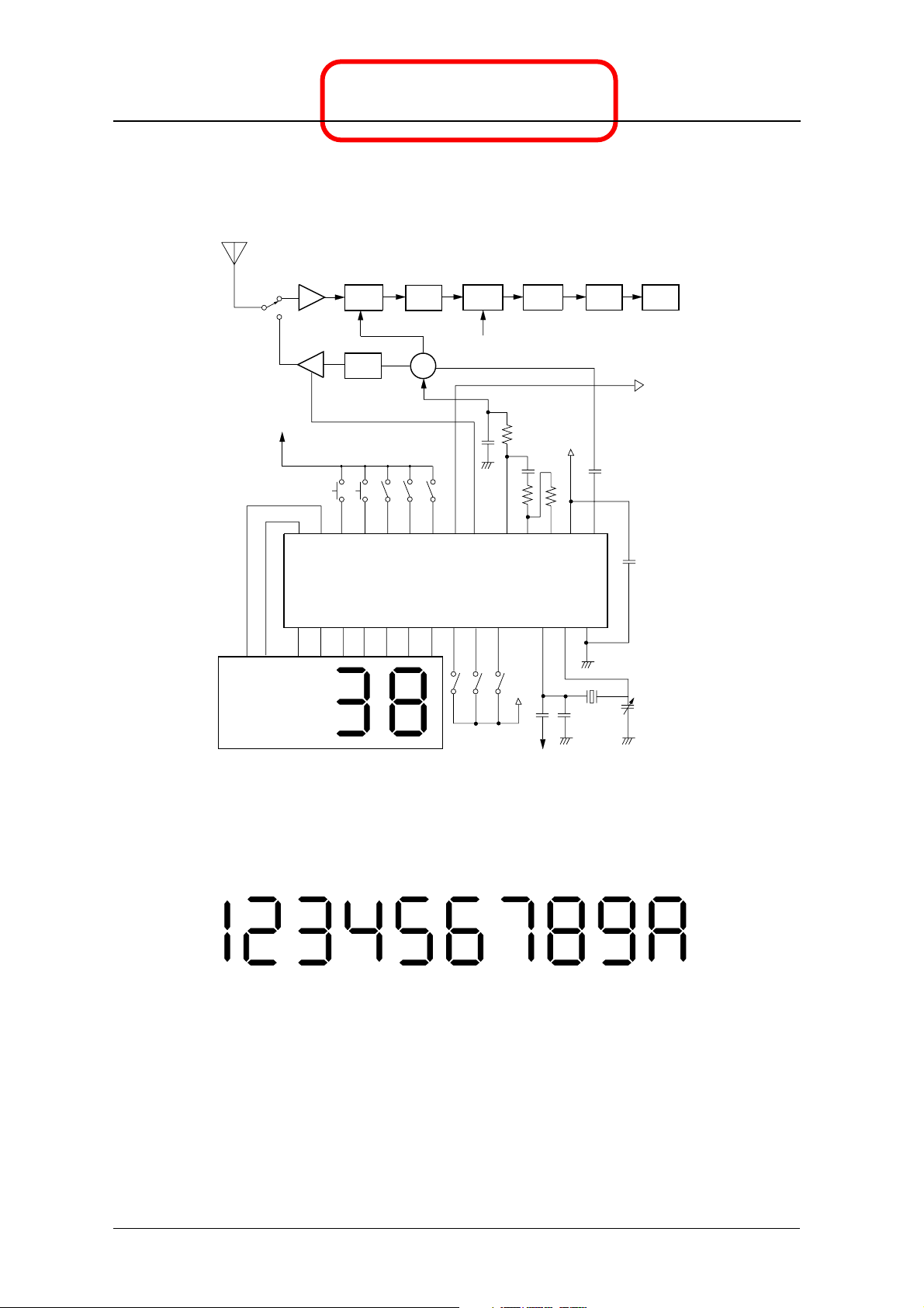
TYPICAL APPLICATION
DISCONTINUED
SM5128A1
PRODUCT
VDD
LOW BATTERY
HIGH POWER
LOW POWER
RF
2
COMB
COMA
COMCS1S2
UP
1ST
MIX
MOD
DN
S3
EMG
S4
1ST
VCO
TR
S5
CE
S6
2ND
MIX
10.24MHz
LD
CHO
HL
LB
IF
2ND
IF
R3
C2
C1
R2
AI
AO
DO
PA
TEST
XOUT
VDD
VDD
R1
PIN
VDD
XIN
VSS
10.24MHz
DET
1000pF
AF
TONE OUT
Display Font
1/3 bias 1/3 duty
2ND MIX
NIPPON PRECISION CIRCUITS—5
Page 6
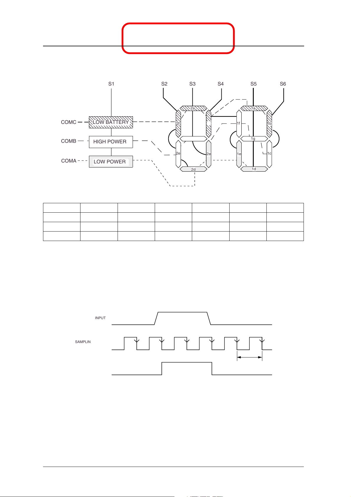
LCD Segment Diagram
DISCONTINUED
SM5128A1
PRODUCT
S1
COMC
COMB
COMA
CommonS1S2S3S4S5S6
COMA LOW POWER 2d 2c 1e 1d –
COMB HIGH POWER 2e 2g 1f 1g 1c
COMC LOW BATTERY 2f 2a 2b 1a 1b
LOW BATTERY
HIGH POWER
LOW POWER
S2
S3 S4
2a
2f
2g
2e
2d
S5 S6
1a
2b
2e
1f
1e
1b
1g
1c
1d
FUNCTIONAL DESCRIPTION
Input Timing
The input timing for pins HL, LB, PA, TR and EMG
is shown in the following figure.
INPUT
SAMPLING CLOCK
(Internal)
INPUT CIRCUITS
OUTPUT
Note that data is read in on the falling edge of the
sampling clock.
51.2ms
NIPPON PRECISION CIRCUITS—6
Page 7
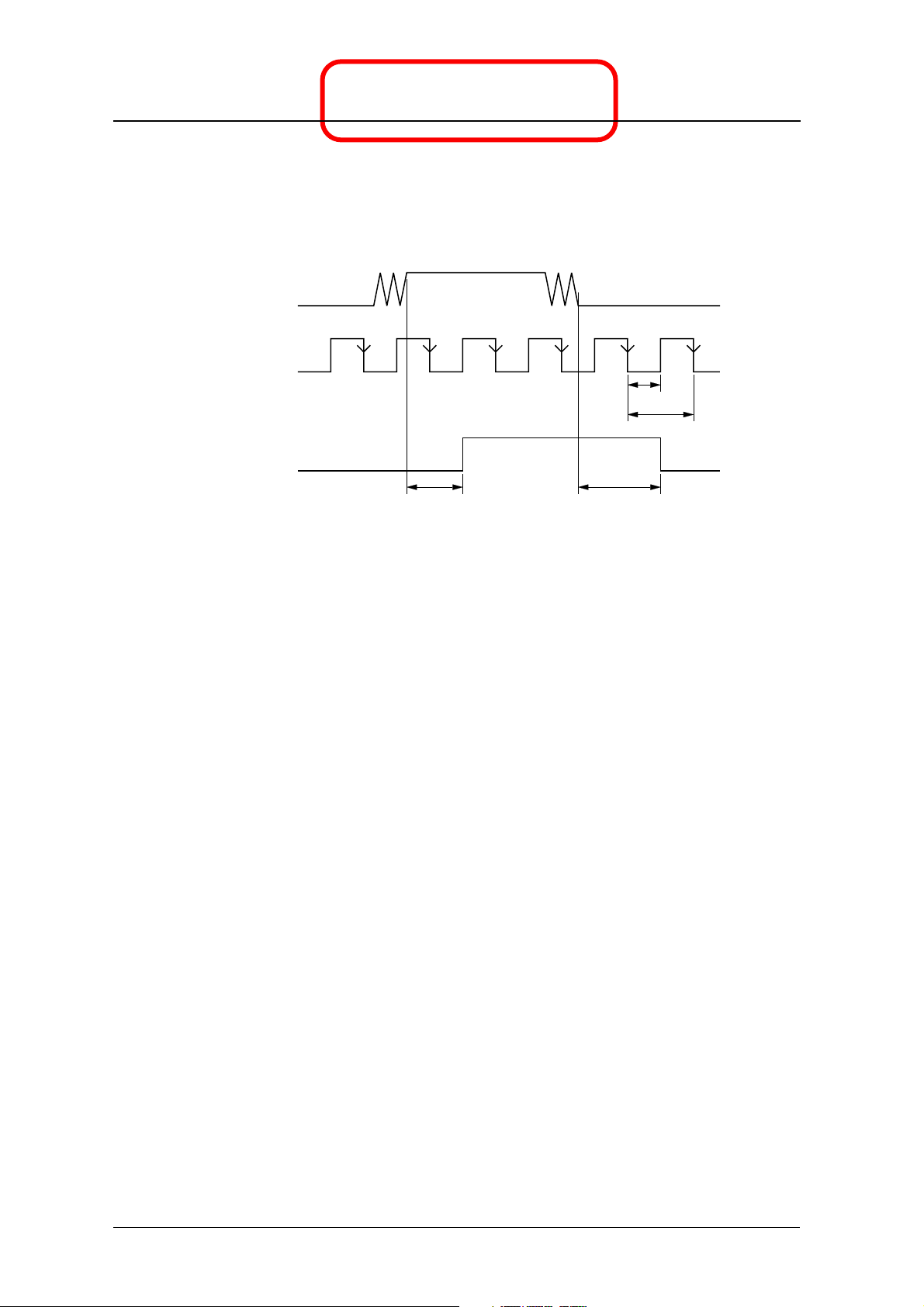
Chattering Elimination Circuit
DISCONTINUED
SM5128A1
PRODUCT
A high-speed chattering elimination circuit is incorporated in pins UP and DN. The chattering elimination circuit recognizes the input state only after the
INPUT
SAMPLING CLOCK
(Internal)
Chatering circuits
OUTPUT
3.2 to 9.6ms
Note that the input is recognized during the LOWlevel pulse interval, t
(32 ms), of the sampling
S
clock.
CE
CE is the chip enable pin. Normal operation is
selected when CE is HIGH, and standby mode is
selected when CE is LOW. CE incorporates a pulldown resistor.
In standby mode, the following states occur.
■ All pins except CE are ignored.
■ Crystal oscillator is stopped. XIN is HIGH, and
XOUT is LOW.
■ PLL operation is stopped. DO and LD are high
impedance, AI and FIN are HIGH, and AO and
CHO are LOW.
■ Display segments are all OFF. COMA, COMB,
COMC, and S1 to S6 are LOW.
■ Current channel selection is stored.
input has been continuously LOW or HIGH for a
period of 3.2 to 6.4 ms. The output does not change
if the input state lasts less than 3.2 ms.
3.2ms(ts)
6.4ms
3.2 to 9.6ms
TR
TR is the transmit/receive select pin. Transmit is
selected when TR is HIGH, and receive is selected
when TR is LOW or open. When transmit mode is
selected, the channel up/down control is disabled,
and the state of pin EMG is accepted. TR incorporates a pull-down resistor.
PA
PA is the PA display mode select pin. PA mode is
selected when pin PA is HIGH. When PA is open,
PLL operation is restored. PA incorporates a pulldown resistor.
In PA display mode, PLL operation is stopped and
the following states occur.
■ FIN and AI are HIGH.
■ CHO is LOW.
■ DO and LD are high impedance.
■ Current channel selection is stored.
■ “HIGH POWER” and “LOW POWER” display
indicators are OFF.
NIPPON PRECISION CIRCUITS—7
Page 8
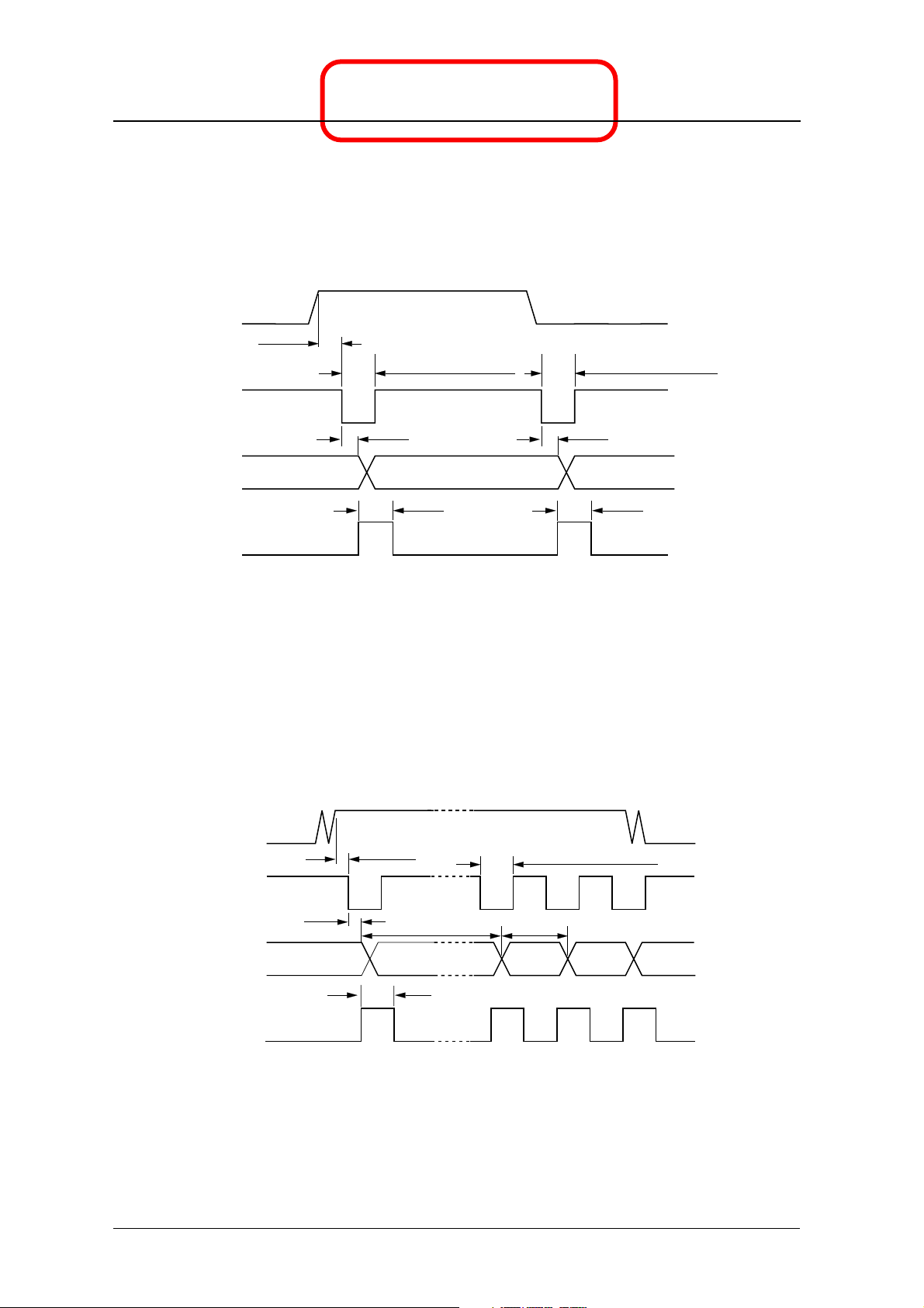
EMG
DISCONTINUED
SM5128A1
PRODUCT
EMG is the emergency channel select pin. The emer gency channel, channel 9, is selected when EMG is
HIGH, and the previously selected channel, deter-
EMG
0 to 51.2ms
25.6ms +Lock up time + 4.8ms
LD
25.6ms
PLL DATA
51.2ms 51.2ms
CHO
UP and DN
mined by the state of pins UP and DN, is selected
when EMG is LOW or open. EMG incorporates a
pull-down resistor.
25.6ms +Lock up time + 4.8ms
25.6ms
UP and DN are the channel up/down control pins,
respectively. They also serve as the fast up/down
function controls, in addition to their step up/down
functions. The fast change function is selected and
the channel change cycle becomes faster when a key
corresponding to either input pin is pressed continuously for a period longer than the wait time t
UP,DN
LD
25.6mS
PLL DATA
.
W
3.2 to 9.6mS
tW=870.4ms
51.2ms
Channel up/down operation is selected when EMG
and PA are LOW. Up/down operation is disabled
when CE is LOW (standby mode) and when TR is
HIGH (transmit mode).
25.6mS +Lock up time + 4.8mS
tF=102.4ms
NIPPON PRECISION CIRCUITS—8
Page 9
LD
DISCONTINUED
SM5128A1
PRODUCT
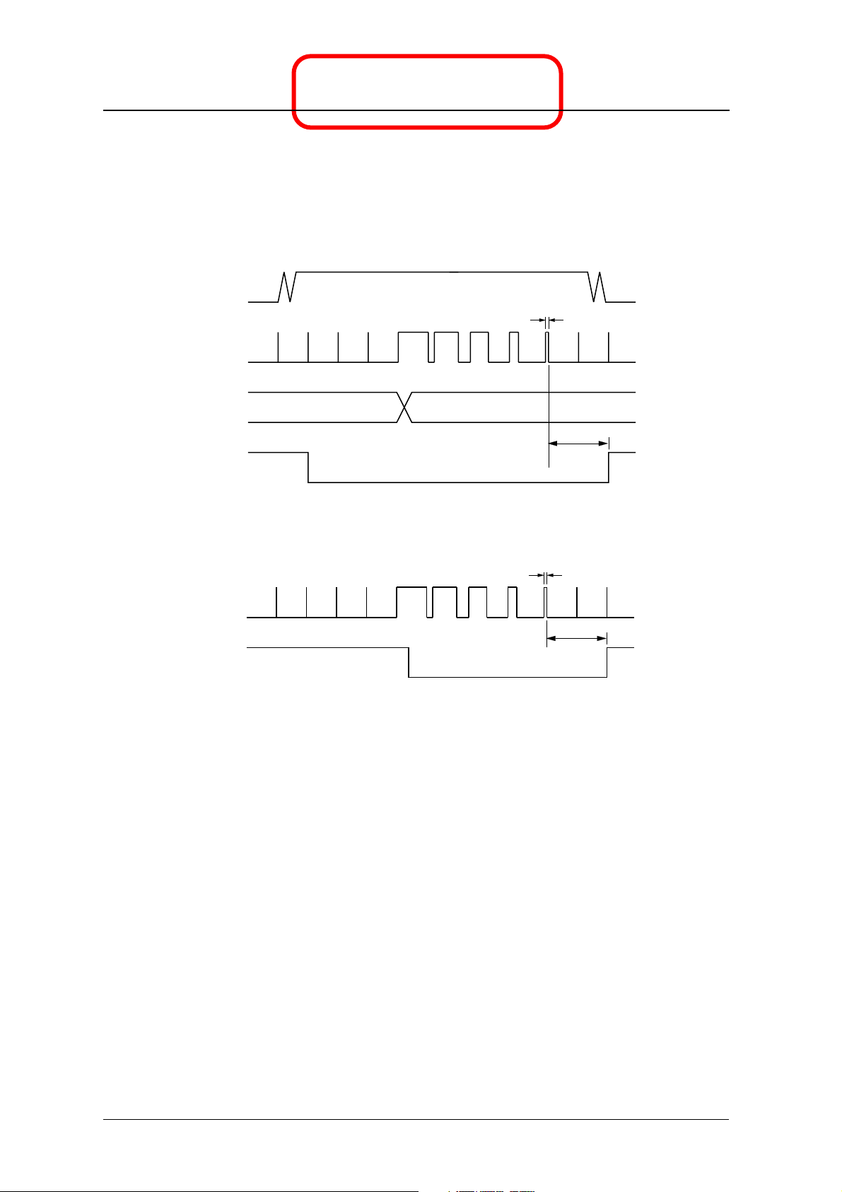
LD is the unlock detector pin. The PLL is locked
when LD is HIGH, and the PLL is unlocked when
LD is LOW.
Inputs are LOW (case 1)
UP,DN
Phase
difference
(internal)
PLL DATA
LD
External disturbance (case 2)
Phase
difference
(internal)
LD goes LOW when UP, DN, TR and EMG are
LOW (case 1), and when the PLL becomes unlocked
due to an external disturbance (case 2).
tPW
tLD
tPW
tLD
LD
When the internal phase difference t
exceeds 1.6
PW
µs, the PLL unlocks and LD goes LOW. Subsequently, when the difference is less than 1.6 µs for a
period of 4.8 ms, the hPLL locks and LD goes
HIGH.
NIPPON PRECISION CIRCUITS—9
Page 10
Input Pin Priority
DISCONTINUED
SM5128A1
PRODUCT
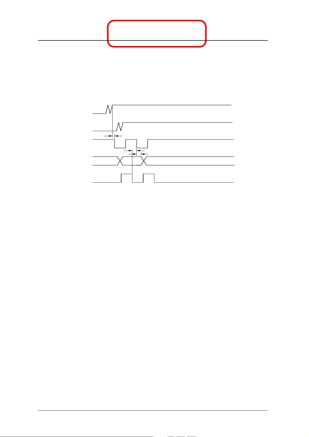
The device operation for all possible input combinations is determined by the active level of the inputs
using the following input pin priority.
CE > PA > EMG > UP > DN
UP,DN
EMG
3.2 to 9.6ms
LD
PLL DATA
CHO
CHO
CHO is the channel change confirmation tone output,
and indicates that the frequency changed due to
switching UP, DN, TR and EMG. The output signal
is a 2.5 kHz tone of approximately 51.2 ms duration.
If a high priority pin goes LOW (active) while a
lower priority pin operation is in progress (from
when LD goes LOW until CHO output stops), the
operation stops and the higher priority pin operation
takes precedence.
25.6ms
25.6ms
CH9
LB
LB is the “LOW BATTERY” display indicator control input. The indicator is lit when LB is LOW or
open, and the indicator is OFF when LB is HIGH.
LB incorporates a pull-down resistor. The state of
LB does not affect PLL operation.
HL
HL is the “HIGH POWER” and “LOW POWER”
display indicators control input. The “HIGH
POWER” indicator is lit when HL is HIGH, and the
“LOW POWER” indicator is lit when HL is LOW or
open. HL incorporates a pull-down resistor. The state
of HL does not affect PLL operation.
NIPPON PRECISION CIRCUITS—10
Page 11
DISCONTINUED
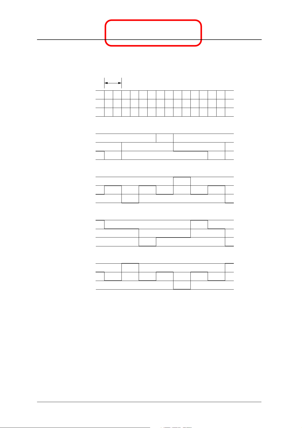
LCD Common/Segment Output
Waveforms
1.6mS
VDD
SM5128A1
PRODUCT
Internal
reffrence clock
COM1
COM2
COM3
VSS3
VSS2
VSS1
VDD
VSS3
VSS2
VSS1
VDD
VSS3
VSS2
VSS1
VDD
VSS3
VSS2
VSS1
VDD
S outoput
VSS3
VSS2
VSS1
Power-ON Initialization
When power is applied between VDD and VSS, the
channel up/down and other controls are disabled in
the current channel is channel 9.
NIPPON PRECISION CIRCUITS—11
Page 12
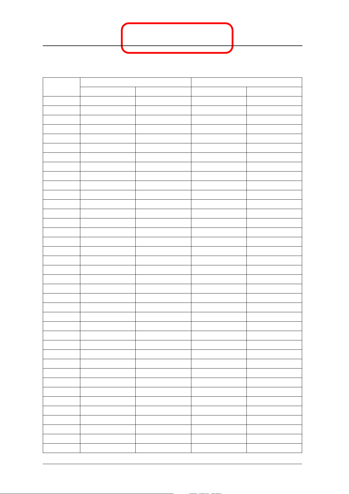
FREQUENCY TABLE
USA-specication
DISCONTINUED
SM5128A1
PRODUCT
Channel
1 5393 13.4825 3254 16.27
2 5395 13.4875 3256 16.28
3 5397 13.4925 3258 16.29
4 5401 13.5025 3262 16.31
5 5403 13.5075 3264 16.32
6 5405 13.5125 3266 16.33
7 5407 13.5175 3268 16.34
8 5411 13.5275 3272 16.36
9 5413 13.5325 3274 16.37
10 5415 13.5375 3276 16.38
11 5417 13.5425 3278 16.39
12 5421 13.5525 3282 16.41
13 5423 13.5575 3284 16.42
14 5425 13.5625 3286 16.43
15 5427 13.5675 3288 16.44
16 5431 13.5775 3292 16.46
17 5433 13.5825 3294 16.47
18 5435 13.5875 3296 16.48
19 5437 13.5925 3298 16.49
20 5441 13.6025 3302 16.51
21 5443 13.6075 3304 16.52
22 5445 13.6125 3306 16.53
23 5451 13.6275 3312 16.56
24 5447 13.6175 3308 16.54
25 5449 13.6225 3310 16.55
26 5453 13.6325 3314 16.57
27 5455 13.6375 3316 16.58
28 5457 13.6425 3318 16.59
29 5459 13.6475 3320 16.60
30 5461 13.6525 3322 16.61
31 5463 13.6575 3324 16.62
32 5465 13.6625 3326 16.63
33 5467 13.6675 3328 16.64
34 5469 13.6725 3330 16.65
35 5471 13.6775 3332 16.66
36 5473 13.6825 3334 16.67
37 5475 13.6875 3336 16.68
38 5477 13.6925 3338 16.69
N (T) VCO (MHz) N (R) VCO (MHz)
TR = HIGH TR = LOW (open)
NIPPON PRECISION CIRCUITS—12
Page 13

DISCONTINUED
SM5128A1
PRODUCT
Channel
39 5479 13.6975 3340 16.70
40 5481 13.7025 3342 16.71
N (T) VCO (MHz) N (R) VCO (MHz)
TR = HIGH TR = LOW (open)
NIPPON PRECISION CIRCUITS—13
Page 14

DISCONTINUED
SM5128A1
PRODUCT
NIPPON PRECISION CIRCUITS INC. reserves the right to make changes to the products contained in this data sheet in order to
improve the design or performance and to supply the best possible products. Nippon Precision Circuits Inc. assumes no responsibility for
the use of any circuits shown in this data sheet, conveys no licence under any patent or other rights, and makes no claim that the circuits
are free from patent infringement. Applications for any devices shown in this data sheet are for illustration only and Nippon
PrecisionCircuits Inc. makes no claim or warranty that such applications will be suitable for the use specified without further testing or
modification.Products contained in this data sheet are not intended to be the devices which mat directly affect human lives due to failure
or malfunction. Customers are requested to consult with the sales department of Nippon Precision Circuits Inc. prior to considering our
products in such a special case.
NIPPON PRECISION CIRCUITS INC.
4-3, 2-chome Fukuzumi
Koto-ku, Tokyo 135, Japan
NIPPON PRECISION CIRCUITS INC.
Telephone: 03-3642-6663
Facsimile: 03-3642-6698
NC9608BE 2001.06
NIPPON PRECISION CIRCUITS—14
 Loading...