

Page 1
SM5021 series
NIPPON PRECISION CIRCUITS INC.
Crystal Oscillator Module ICs
OVERVIEW
The SM5021 series are crystal oscillator module ICs
fabricated in NPC’s Molybdenum-gate CMOS, that
incorporate high-frequency, low current consumption oscillator and output buffer circuits. Highly
accurate thin-film feedback resistors and high-frequency capacitors are built-in, eliminating the need
for external components to make a stable 3rd-harmonic oscillator.
FEATURES
■
3rd overtone oscillation
■
Capacitors CG, CD built-in
■
Inverter amplifier feedback resistor built-in
(A × , B × series)
■
TTL input level
■
4 mA (V
8 mA (V
= 2.7 V) drive capability
DD
= 4.5 V) drive capability
DD
■
Output three-state function
■
2.7 to 5.5 V supply voltage (A × , K × series)
4.5 to 5.5 V supply voltage (B × , L × series)
■
Oscillator frequency output
■
6-pin SOT (SM5021 ×× H)
■
Chip form (CF5021 ×× )
SERIES CONFIGURATION
Supply voltage
1
Version
Chip SOT 3V 5V C
SM5021AAH 4.5 to 5.5 4.5 to 5.5
SM5021ABH 2.7 to 5.5 2.7 to 5.5 22 to 30 30 to 43 8 15 1 3.3 fo CMOS High impedance
SM5021ACH 2.7 to 5.5 2.7 to 5.5 30 to 40 43 to 55 8 15 2 3.9 fo CMOS High impedance
SM5021ADH 2.7 to 5.5 2.7 to 5.5 40 to 50 55 to 70 8 15 3 2.7 fo CMOS High impedance
SM5021AEH 2.7 to 3.6
SM5021BAH 4.5 to 5.5 4.5 to 5.5
SM5021BBH 4.5 to 5.5 4.5 to 5.5
SM5021BCH 4.5 to 5.5 4.5 to 5.5
SM5021BDH 4.5 to 5.5 4.5 to 5.5
SM5021KDH 2.7 to 5.5 2.7 to 5.5 22 to 50 22 to 70 8 15 3 – fo CMOS High impedance
SM5021KEH 2.7 to 3.6 2.7 to 3.6 50 to 70
SM5021LDH 4.5 to 5.5 4.5 to 5.5
1. Chip form devices have designation CF5021 ×× .
×
Recommended
operating frequency
range (MHz)
×
22 to 30 8 15 1 6.0 fo CMOS High impedance
50 to 70
×
×
×
×
×
×
22 to 30 8 15 1 6.0 fo TTL High impedance
30 to 43 8 15 1 3.3 fo TTL High impedance
43 to 55 8 15 2 3.9 fo TTL High impedance
55 to 70 8 15 3 2.7 fo TTL High impedance
×
22 to 70 8 15 3 – fo TTL High impedance
Built-in
capacitance
(pF)
G
8 12 4 2.7 fo CMOS High impedance
8 12 4 – fo CMOS High impedance
C
D
gm
ratioRf(k Ω )
Output
frequency
Output
level
Standby output
state
ORDERING INFORMATION
Devicez Package
SM5021 ×× H 6-pin SOT
CF5021 ×× –2 Chip form
NIPPON PRECISION CIRCUITS—1
Page 2
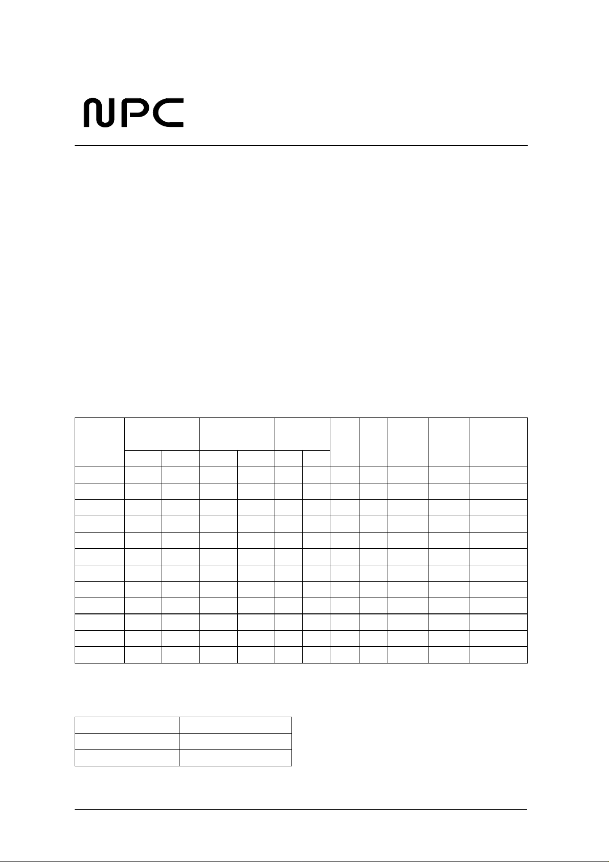
•
PACKAGE DIMENSIONS
(UNIT : mm)
6-pin SOT
SM5021 series
2.9 ± 0.2
1.9 ± 0.2
0.95
0.4 ± 0.1
0.12
+ 0.2
1.1 ± 0.1
0.1
M
− 0.1
1.6
− 0.3
+ 0.2
2.8
0 to 0.15
0.45 ± 0.15
0.15
+
−
0.1
0.05
NIPPON PRECISION CIRCUITS—2
Page 3
SM5021 series
PAD LAYOUT
(Unit : µ m)
Q
(0,0)
Chip size: 1.00 × 0.80 mm
Chip thickness: 220 ± 30 µm
Chip base: V
HA5021
XTVSS
INH
level
DD
XT
(1000,800)
VDD
PINOUT
(T op V iew)
INH
XT
VSS
1
6
1
2
3
5
4
PIN DESCRIPTION and PAD DIMENSIONS
Number Name I/O Description
1 INH I Output state control input. High impedance when LOW. Pull-up resistor built in 771 150
2 XT I Amplifier input.
3 VSS – Ground 150 140
4 Q O Output. Output frequency (f
5 VDD – Supply voltage 796 409
6XT
O Amplifier output.
Crystal oscillator connection pins.
Crystal oscillator connected between XT and XT
) 150 649
O
Crystal oscillator connection pins.
Crystal oscillator connected between XT and XT
Pad dimensions [µm]
XY
553 150
836 636
XT
VDD
Q
BLOCK DIAGRAM
XT
XT
INH
VSSVDD
CG CD
Rf
Q
NIPPON PRECISION CIRCUITS—3
Page 4
SPECIFICATIONS
Absolute Maximum Ratings
V
= 0 V
SS
Parameter Symbol Condition Rating Unit
Supply voltage range V
Input voltage range V
Output voltage range V
Operating temperature range T
Storage temperature range T
Output current I
Power dissipation P
DD
OUT
opr
stg
OUT
≤
−
−
−
−
−
SM5021 series
0.5 to 7.0 V
0.5 to V
IN
Chip form
6-pin SOT
D
6-pin SOT 250 mW
+ 0.5 V
DD
0.5 to V
+ 0.5 V
DD
40 to 85
− 65 to 150
− 55 to 125
13 mA
° C
° C
Recommended Operating Conditions
V
= 0 V, f ≤ 70MHz, C
SS
Parameter Symbol Condition
Supply voltage V
Input voltage V
Operating temperature T
Note: Recommended operating conditions will change in accordance with operating frequency, load capacitance, or power dissipation.
L
15pF
DD
IN
OPR
Rating
min typ max
2.7 – 5.5 V
V
SS
–V
DD
20 – 80
Unit
V
° C
NIPPON PRECISION CIRCUITS—4
Page 5

SM5021 series
Electrical Characteristics
3 V operation: AA, AB, AC, AD, AE series/ KD, KE series
V
= 2.7 to 3.6 V, V
DD
= 0 V, Ta = − 20 to 80 ° C unless otherwise noted.
SS
Parameter Symbol Condition
Q: Measurement cct 1, V
I
= 4 mA
HIGH-level output voltage V
OH
OH
Q: Measurement cct 1, V
I
= 8 mA
OH
Q: Measurement cct 2, V
I
= 4 mA
LOW-level output voltage V
OL
OL
Q: Measurement cct 2, V
I
= 8 mA
OL
Output leakage current I
HIGH-level input voltage V
LOW-level input voltage V
Q: Measurement cct 2, V
Z
Q: Measurement cct 2, V
INH 2.0 – – V
IH
INH – – 0.5 V
IL
INH = open, Measurement cct 3,
Current consumption I
INH pull-up resistance R
Feedback resistance
(A × series only)
Built-in capacitance
load cct 1, C
DD
70 MHz crystal oscillator
Measurement cct 4 25 100 250 k Ω
UP
Measurement cct 5
R
f
C
Design value, determined by the internal wafer pattern 7.44 8 8.56 pF
G
Design value, determined by the
C
D
internal wafer pattern
= 15 pF,
L
SM5021 × AH, CF5021 × A
DD
= 2.7 V,
SM5021 × BH, CF5021 × B
SM5021 × CH, CF5021 × C
SM5021 × DH, CF5021 × D
= 2.7 V,
DD
SM5021 ×
SM5021 × AH, CF5021 × A
DD
= 2.7 V,
SM5021 × BH, CF5021 × B
SM5021 × CH, CF5021 × C
SM5021 × DH, CF5021 × D
= 2.7 V,
DD
= 3.3 V, INH = LOW, V
DD
= 3.3 V, INH = LOW, V
DD
SM5021 ×
SM5021A
SM5021K
SM5021
SM5021 × BH, CF5021 × B 2.8 3.3 3.8
SM5021 × CH, CF5021 × C 3.3 3.9 4.5
SM5021 ×
SM5021 × EH, CF5021 × E
SM5021 × AH, CF5021 × A
SM5021 × BH, CF5021 × B
SM5021 × CH, CF5021 × C
SM5021 × DH, CF5021 × D
SM5021 × EH, CF5021 × E 11.16 12 12.84
Rating
min typ max
2.1 2.4 – V
EH, CF5021
× E
– 0.3 0.4 V
EH, CF5021
OH
OL
×
H, CF5021A
× H, CF5021K
×
AH, CF5021 × A 5.1 6.0 6.9
DH, CF5021 × D
= V
= V
× E
DD
SS
––10
––10
×
–1325mA
×
2.3 2.7 3.1
13.95 15 16.05
Unit
µA
k Ω
pF
NIPPON PRECISION CIRCUITS—5
Page 6

SM5021 series
5 V operation: AA, AB, AC, AD series/ BA, BB, BC, BD series/ KD series/ LD series
V
= 4.5 to 5.5 V, V
DD
= 0 V, Ta = − 20 to 80 ° C unless otherwise noted.
SS
Parameter Symbol Condition
HIGH-level output voltage V
LOW-level output voltage V
Output leakage current I
HIGH-level input voltage V
LOW-level input voltage V
Q: Measurement cct 1, V
OH
Q: Measurement cct 2, V
OL
Q: Measurement cct 2, V
Z
Q: Measurement cct 2, V
INH 2.0 – – V
IH
INH – – 0.8 V
IL
INH = open, Measurement cct 3,
Current consumption I
load cct 1, C
70 MHz crystal oscillator
DD
= 15 pF,
L
INH = open, Measurement cct 3,
INH pull-up resistance R
Feedback resistance
(A
× , B
× series only)
Built-in capacitance
load cct 2, C
70 MHz crystal oscillator
Measurement cct 4 25 100 250 k Ω
UP
Measurement cct 5
R
f
C
G
Design value, determined by the
internal wafer pattern
C
D
= 15 pF,
L
= 4.5 V, I
DD
= 4.5 V, I
DD
= 5.5 V, INH = LOW, V
DD
= 5.5 V, INH = LOW, V
DD
= 8 mA 3.9 4.2 – V
OH
= 8 mA – 0.3 0.4 V
OL
SM5021AAH, CF5021AA
SM5021ABH, CF5021AB
SM5021ACH, CF5021AC
SM5021ADH, CF5021AD
SM5021KDH, CF5021KD
SM5021B
SM5021L
SM5021 × AH, CF5021 × A 5.1 6.0 6.9
SM5021 × BH, CF5021 × B 2.8 3.3 3.8
SM5021 × CH, CF5021 × C 3.3 3.9 4.5
SM5021 × DH, CF5021 × D 2.3 2.7 3.1
SM5021 × AH, CF5021 × A
SM5021 × BH, CF5021 × B
SM5021 × CH, CF5021 × C
SM5021 × DH, CF5021 × D
= V
OH
DD
= V
OL
SS
×
H, CF5021B
× H, CF5021L
Rating
min typ max
––10
––10
–1835
×
–1835
×
7.44 8 8.56 pF
13.95 15 16.05 pF
Unit
µA
mA
k Ω
NIPPON PRECISION CIRCUITS—6
Page 7

SM5021 series
Switching Characteristics
CMOS
3 V operation: AA, AB, AC, AD, AE series/ KD, KE series
VDD = 2.7 to 3.6 V, VSS = 0 V, Ta = −20 to 80 °C unless otherwise noted.
Parameter Symbol Condition
Measurement cct 6, load cct 1,
Output rise time t
0.1VDD to 0.9V
r1
DD
Measurement cct 6, load cct 1,
to 0.8V
0.2V
DD
DD
Measurement cct 6, load cct 1,
Output fall time t
0.9VDD to 0.1V
f1
DD
Measurement cct 6, load cct 1,
to 0.2V
0.8V
DD
DD
Output duty cycle
1
Output disable delay time t
Output enable delay time t
Measurement cct 6, load cct 1,
Duty
Ta = 25 °C, VDD = 3 V, CL = 15 pF, f ≤ 70MHz
PLZ
Measurement cct 6, load cct 1, Ta = 25 °C, VDD = 3 V, CL = 15 pF
PZL
1. Determined by the lot monitor.
, CL = 15 pF
, CL = 15 pF
, CL = 15 pF
, CL = 15 pF
SM5021AAH, CF5021AA
SM5021ABH, CF5021AB
SM5021ACH, CF5021AC
SM5021ADH, CF5021AD
SM5021KDH, CF5021KD
SM5021AEH, CF5021AE
SM5021KEH, CF5021KE
SM5021AAH, CF5021AA
SM5021ABH, CF5021AB
SM5021ACH, CF5021AC
SM5021ADH, CF5021AD
SM5021KDH, CF5021KD
SM5021AAH, CF5021AA
SM5021ABH, CF5021AB
SM5021ACH, CF5021AC
SM5021ADH, CF5021AD
SM5021KDH, CF5021KD
SM5021AEH, CF5021AE
SM5021KEH, CF5021KE
SM5021AAH, CF5021AA
SM5021ABH, CF5021AB
SM5021ACH, CF5021AC
SM5021ADH, CF5021AD
SM5021KDH, CF5021KD
Rating
Unit
min typ max
–510
– 3.5 7
ns
– 3.5 7
–510
– 3.5 7
ns
– 3.5 7
45–55%
– – 100 ns
– – 100 ns
5 V operation: AA, AB, AC, AD series/ KD series
VDD = 4.5 to 5.5 V, VSS = 0 V, Ta = −20 to 80 °C unless otherwise noted.
Parameter Symbol Condition
Output rise time t
Output fall time t
Output duty cycle
1
Output disable delay time t
Output enable delay time t
1. Determined by the lot monitor.
Measurement cct 6, load cct 1, 0.1VDD to 0.9V
r1
Measurement cct 6, load cct 1, 0.9VDD to 0.1V
f1
Measurement cct 6, load cct 1,
Duty
Ta = 25 °C, VDD = 5 V, CL = 15 pF, f ≤ 70 MHz
PLZ
Measurement cct 6, load cct 1, Ta = 25 °C, VDD = 5 V, CL = 15 pF
PZL
, CL = 15 pF – 3.5 7 ns
DD
, CL = 15 pF – 3.5 7 ns
DD
Rating
Unit
min typ max
45–55%
– – 100 ns
– – 100 ns
NIPPON PRECISION CIRCUITS—7
Page 8

SM5021 series
TTL
5 V operation: BA, BB, BC, BD series/ LD series
VDD = 4.5 to 5.5 V, VSS = 0 V, Ta = −20 to 80 °C unless otherwise noted.
Parameter Symbol Condition
Output rise time t
Output fall time t
Output duty cycle
Output disable delay time t
Output enable delay time t
1. Determined by the lot monitor.
1
Measurement cct 6, load cct 2, 0.4V to 2.4V, CL = 15 pF – 2.5 7 ns
r2
Measurement cct 6, load cct 2, 2.4V to 0.4V, CL = 15 pF – 2.5 7 ns
f2
Measurement cct 6, load cct 2,
Duty
Ta = 25 °C, V
PLZ
Measurement cct 6, load cct 2, Ta = 25 °C, VDD = 5 V, CL = 15 pF
PZL
= 5 V, CL = 15 pF, f ≤ 70 MHz
DD
Rating
min typ max
45–55%
– – 100 ns
– – 100 ns
Current consumption and Output waveform with NPC’s standard crystal
f (MHz) R (Ω) L (mH) Ca (fF) Cb (pF)
30 18.62 16.24 1.733 5.337
40 20.53 11.34 1.396 3.989
50 22.17 7.40 1.370 4.105
60 22.20 5.05 1.388 4.226
70 25.42 4.18 1.254 5.170
L
Cb
Ca R
FUNCTIONAL DESCRIPTION
Unit
Standby Function
When INH goes LOW, the oscillator output on Q goes high impedance.
INH Q Oscillator
HIGH (or open) fO output frequency Normal operation
LOW High impedance Normal operation
NIPPON PRECISION CIRCUITS—8
Page 9

MEASUREMENT CIRCUITS
SM5021 series
Measurement cct 1
Signal
Generator
Q out monitor
2.0V
, 10MHz sine wave input signal (3V operation)
P−P
3.5V
, 10MHz sine wave input signal (5V operation)
P−P
C1 : 0.001µF
C1
R1 R2
XT Q
R3
XT
VDD
VSS
VOH
0V
Measurement cct 4
5.0V
VDD
VSS
R1 : 50Ω
R2 : 525Ω (3V operation/ ×A, ×B, ×C, ×D series)
263Ω (3V operation/ ×E series)
490Ω (5V operation)
R3 : 100kΩ (K×, L× series)
Measurement cct 2 Measurement cct 5
INH
A
IPR
RUP =
DD
V
IPR
VDD
VSS
INH
Measurement cct 3
Signal
Generator
C1
R1
Q
V
XT Q
R3
XT
IOL, IZ
IZ
VOL
VDD
VSS
VDD
XT
A
XT
VSS
Rf =
DD
V
IRf
A
IRf
Measurement cct 6
IDD
XT
Rfo
XT
INH
A
VDD
IDD
IST
QX'tal
VSS
2.0V
, 70MHz sine wave input signal (3V operation)
P−P
3.5V
, 70MHz sine wave input signal (5V operation)
P−P
C1 : 0.001µF
R1 : 50Ω
R3 : 100kΩ (K×, L× series)
Rfo : 2.7kΩ (K×, L× series)
NIPPON PRECISION CIRCUITS—9
Page 10

SM5021 series
Load cct 1
Q output
CL
(Including probe capacity)
CL = 15pF: tr1, t
f1
Switching Time Measurement Waveform
Output duty level (CMOS)
0.9VDD
Q output
0.1VDD
tr tf
TW
Load cct 2
Q output
CL = 15pF: t
R = 800Ω
0.9VDD
(Including proove
, t
r2
0.1VDD
capacity)
f2
L
C
DUTY measuring
voltage (0.5V
DD)
R
Output duty level (TTL)
Q output
Output duty cycle (CMOS)
Q output
Output duty cycle (TTL)
Q output
2.4V
0.4V
TW
tr tf
TW
T
TW
2.4V
0.4V
DUTY measuring
voltage (1.4V
DUTY measuring
voltage
DUTY= T
W/ T 100 (%)
DUTY measuring
voltage
)
(0.5VDD)
(1.4V)
T
DUTY= T
NIPPON PRECISION CIRCUITS—10
W/ T 100 (%)
Page 11

Output Enable/Disable Delay
SM5021 series
INH
Q output
VIL
tPLZ
INH inputwaveform tr = tf 10ns
VIH
tPZL
NIPPON PRECISION CIRCUITS INC. reserves the right to make changes to the products described in this data sheet in order to
improve the design or performance and to supply the best possible products. Nippon Precision Circuits Inc. assumes no responsibility for
the use of any circuits shown in this data sheet, conveys no license under any patent or other rights, and makes no claim that the circuits
are free from patent infringement. Applications for any devices shown in this data sheet are for illustration only and Nippon Precision
Circuits Inc. makes no claim or warr anty that such applications will be suitab le for the use specified without further testing or modification.
The products described in this data sheet are not intended to use for the apparatus which influence human lives due to the failure or
malfunction of the products. Customers are requested to comply with applicable laws and regulations in effect now and hereinafter,
including compliance with export controls on the distribution or dissemination of the products. Customers shall not expor t, directly or
indirectly, any products without first obtaining required licenses and approvals from appropriate government agencies.
NIPPON PRECISION CIRCUITS INC.
4-3, Fukuzumi 2-chome
Koto-ku, Tokyo 135-8430, Japan
NIPPON PRECISION CIRCUITS INC.
Telephone: 03-3642-6661
Facsimile: 03-3642-6698
NC9903AE 1999.11
NIPPON PRECISION CIRCUITS—11
 Loading...