

Page 1
SMJ320MCM42C, SMJ320MCM42D
DUAL SMJ320C40 MULTICHIP MODULE
SGKS001B – JULY 1997 – REVISED FEBRUARY 2000
1
POST OFFICE BOX 1443 • HOUSTON, TEXAS 77251–1443
D Performance:
– 80 Million Floating-Point Operations Per
Second (MFLOPS) With 496-MBps-Burst
I/O Rate for 40-MHz Modules
– Zero-Wait-State Local Memory for Each
Processor
D Organization:
– 128K-Word × 32-Bit Static
Random-Access Memory (SRAM)
(SMJ320MCM42D)
– 256K-Word × 32-Bit SRAM
(SMJ320MCM42C)
D Compliant With MIL-PRF-38535 QML
D Dual ’C40 Performance With Local Memory
Requiring Only 8.7 Square Inches of Board
Space
D Enhanced Performance Offered By
Multichip-Module Solution
– SMJ320MCM42C
– 67% Reduction in Number of
Interconnects
– 54% Reduction (Minimum) in Board
Area
– Estimated 38% Reduction in Power
Dissipation Due to Reduced Parasitic
Capacitance and Interconnect Lengths
– SMJ320MCM42D
– 56% Reduction in Number of
Interconnects
– 30% Reduction (Minimum) in Board
Area
– Estimated 20% Reduction in Power
Dissipation Due to Reduced Parasitic
Capacitance and Interconnect Lengths
D Four Memory Ports for High Data
Bandwidth
– Two Full 2G-Word External Buses
D Two Internal Buses Mapped to Memory
– 128K-Word × 32-Bit SRAM for Each ’C40
Local Bus (SMJ320MCM42D)
– 256K-Word × 32-Bit SRAM for Each ’C40
Local Bus (SMJ320MCM42C)
D Ten External Communication Ports for
Direct Processor-to-Processor
Communication
D IEEE-1149.1
†
(JTAG) Boundary-Scan
Compatible
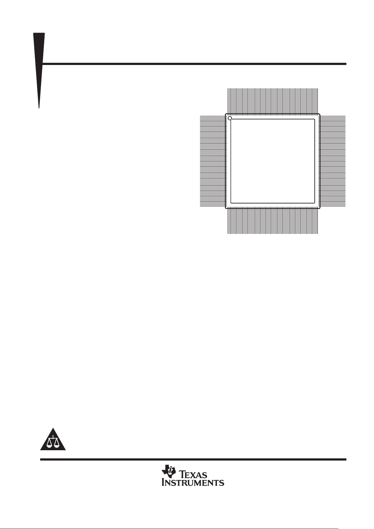
D 408-Lead Ceramic Quad Flatpack Package
(HFN Suffix)
D Operating Free-Air Temperature Ranges:
–55°C to 125°C . . . (Military)
0°C to 70°C . . . (Commercial)
D Communication-Port Connection Provided
Between ’C40s for Interprocessor
Communication
Please be aware that an important notice concerning availability, standard warranty, and use in critical applications of
Texas Instruments semiconductor products and disclaimers thereto appears at the end of this data sheet.
‡
Terminal assignment information is provided by the terminal
assignments table. Package is shown for pinout reference only.
HFN PACKAGE
‡
(TOP VIEW)
306
1
102 205
408 307
103 204
PRODUCTION DATA information is current as of publication date.
Products conform to specifications per the terms of Texas Instruments
standard warranty. Production processing does not necessarily include
testing of all parameters.
Copyright 2000, Texas Instruments Incorporated
†
IEEE Standard 1149.1–1990 Standard Test-Access Port and Boundary-Scan Architecture
On products compliant to MIL-STD-PRF-38535, all parameters
are tested unless otherwise noted. On all other products,
production processing does not necessarily include testing of all
parameters.
Page 2

SMJ320MCM42C, SMJ320MCM42D
DUAL SMJ320C40 MULTICHIP MODULE
SGKS001B – JULY 1997 – REVISED FEBRUARY 2000
2
POST OFFICE BOX 1443 • HOUSTON, TEXAS 77251–1443
description
The ’42 dual ’C40 multichip module (MCM) contains two SMJ320C40 digital signal processors (DSPs) with
128K words × 32 bits (’42D) or 256K words × 32 bits (’42C) of zero-wait-state SRAMs mapped to each local
bus. Global address and data buses with two sets of control signals are routed externally for each processor,
allowing external memory to be accessed. The external global bus provides a continuous address reach of
2G words.
The dual ’C40 configuration allows standard microprocessor initialization using the bootstrap loader. Both
reset-vector-control terminals are brought out to external terminals for each processor. A single CLKIN line and
a RESET line feed both processors in parallel, minimizing clock skew and allowing easy synchronization for
interlocked operations.
Communication port 0 of CPU #1 connects to communication port 3 of CPU #2 for direct processor-to-processor
communication.
The IEEE-1 149.1 (JT AG) test ports of the ’C40s are connected serially to allow scan operations and emulation
of the module as a whole. T estability of the ’42 adds value and reduces development and support costs. Texas
Instruments (TI) offers a wide variety of ANSI/IEEE-1149.1 products and support.
The ’42 dual ’C40 MCM is packaged in a 408-pin ceramic quad flat pack. The ’42 dual ’C40 MCM is available
in both a commercial temperature range (0°C to 70°C) and a military temperature range (–55°C to 125°C)
option.
TI is a trademark of Texas Instruments Incorporated.
Page 3
SMJ320MCM42C, SMJ320MCM42D
DUAL SMJ320C40 MULTICHIP MODULE
SGKS001B – JULY 1997 – REVISED FEBRUARY 2000
3
POST OFFICE BOX 1443 • HOUSTON, TEXAS 77251–1443
device symbol nomenclature
Example: SMJ 320 MCM 4 2 C HFN M 40
Process-Level Prefix
(See Table 1)
320 DSP Family Designator
Multichip Module
Processor Family
Number of CPUs per Module
Module Revision
Package
HFN = 408-Lead Ceramic Quad Flatpack
Temperature Range
L=0°C to 70°C
M= –55°C to 125°C
Speed Designator
40 = 40 MHz
’42C = 256K-word × 32-bit SRAM
’42D = 128K-word
× 32-bit SRAM
Table 1. MCM Processing Matrix
PROCESS
LEVEL
TEMPERATURE RANGE DIE
100%
PROCESSED
SPEED
TEST
TEST
TEMPERATURE
RANGE
QUALIFICATION
TESTING
L version 0°C to 70°C Probed No No 25°C to 70°C Package
SM
M version –55°C to 125°C Probed No Yes –55°C to 125°C Package
SMJ
†
M version –55°C to 125°C KGD
‡
Yes Yes –55°C to 125°C MIL-H-38534
†
SMJ-level product is full MIL-PRF-38535 QML compliant.
‡
KGD stands for the known-good-die strategy as defined in the reference documentation section.
Page 4
SMJ320MCM42C, SMJ320MCM42D
DUAL SMJ320C40 MULTICHIP MODULE
SGKS001B – JULY 1997 – REVISED FEBRUARY 2000
4
POST OFFICE BOX 1443 • HOUSTON, TEXAS 77251–1443
Terminal Assignments
TERMINAL TERMINAL TERMINAL TERMINAL
NO. NAME NO. NAME NO. NAME NO. NAME
1
2
3
4
5
6
7
8
9
10
11
12
13
14
15
16
17
18
19
20
21
22
23
24
25
26
27
28
29
30
31
32
33
34
35
36
37
38
39
40
41
42
43
44
45
46
47
48
49
50
51
ROMEN_C40_#1
IIOF0_C40_#1
IIOF1_C40_#1
IIOF2_C40_#1
IIOF3_C40_#1
NMI_C40_#1
VCC_DR
VSS_CL
TCLK0_C40_#1
TCLK1_C40_#1
H3_C40_#1
H1_C40_#1
VSS_CL
IACK_C40_#1
CLKIN_COMM
VCC_DR
VCC_CL
VCC_DR
VSS_CL
VSS_DR
VCC_DR
VCC_DR
VCC_CL
VSS_CL
VSS_DR
VSS_CL
VCC_DR
A30_C40_#1
A29_C40_#1
A28_C40_#1
VCC_DR
A27_C40_#1
A26_C40_#1
A25_C40_#1
A24_C40_#1
A23_C40_#1
A22_C40_#1
A21_C40_#1
A20_C40_#1
A19_C40_#1
A18_C40_#1
A17_C40_#1
VCC_DR
VSS_CL
VSS_DR
A16_C40_#1
A15_C40_#1
A14_C40_#1
A13_C40_#1
A12_C40_#1
A11_C40_#1
52
53
54
55
56
57
58
59
60
61
62
63
64
65
66
67
68
69
70
71
72
73
74
75
76
77
78
79
80
81
82
83
84
85
86
87
88
89
90
91
92
93
94
95
96
97
98
99
100
101
102
A10_C40_#1
A9_C40_#1
A8_C40_#1
A7_C40_#1
A6_C40_#1
A5_C40_#1
A4_C40_#1
VCC_DR
A3_C40_#1
A2_C40_#1
A1_C40_#1
A0_C40_#1
D31_C40_#2
D30_C40_#2
D29_C40_#2
D28_C40_#2
D27_C40_#2
D26_C40_#2
VCC_DR
D25_C40_#2
D24_C40_#2
D23_C40_#2
D22_C40_#2
D21_C40_#2
D20_C40_#2
D19_C40_#2
D18_C40_#2
D17_C40_#2
D16_C40_#2
VSS_CL
VSS_CL
VCC_DR
VSS_DR
D15_C40_#2
D14_C40_#2
D13_C40_#2
D12_C40_#2
D11_C40_#2
D10_C40_#2
D9_C40_#2
D8_C40_#2
D7_C40_#2
D6_C40_#2
D5_C40_#2
VCC_DR
D4_C40_#2
D3_C40_#2
D2_C40_#2
D1_C40_#2
D0_C40_#2
CE1_C40_#2
103
104
105
106
107
108
109
110
111
112
113
114
115
116
117
118
119
120
121
122
123
124
125
126
127
128
129
130
131
132
133
134
135
136
137
138
139
140
141
142
143
144
145
146
147
148
149
150
151
152
153
RDY1_C40_#2
VSS_DR
VSS_CL
LOCK_C40_#2
VCC_CL
VSS_CL
CE0_C40_#2
RDY0_C40_#2
DE_C40_#2
TCK_COMM
TDO_C40_#2
TMS_COMM
TRST_COMM
EMU0_COMM
EMU1_COMM
PAGE1_C40_#2
R/W
1_C40_#2
STRB1_C40_#2
STAT0_C40_#2
STAT1_C40_#2
VSS_CL
STAT2_C40_#2
STAT3_C40_#2
PAGE0_C40_#2
R/W0_C40_#2
STRB0_C40_#2
AE_C40_#2
RESETLOC1_C40_#2
VCC_DR
RESETLOC0_C40_#2
RESET_COMM
CRDY5_C40_#2
CSTRB5_C40_#2
CACK5_C40_#2
CREQ5_C40_#2
CRDY4_C40_#2
CSTRB4_C40_#2
CACK4_C40_#2
CREQ4_C40_#2
VCC_DR
C5D7_C40_#2
C5D6_C40_#2
C5D5_C40_#2
C5D4_C40_#2
C5D3_C40_#2
C5D2_C40_#2
C5D1_C40_#2
C5D0_C40_#2
VCC_DR
C4D7_C40_#2
C4D6_C40_#2
154
155
156
157
158
159
160
161
162
163
164
165
166
167
168
169
170
171
172
173
174
175
176
177
178
179
180
181
182
183
184
185
186
187
188
189
190
191
192
193
194
195
196
197
198
199
200
201
202
203
204
C4D5_C40_#2
C4D4_C40_#2
C4D3_C40_#2
C4D2_C40_#2
C4D1_C40_#2
C4D0_C40_#2
VCC_DR
VCC_DR
VSS_CL
C2D7_C40_#2
C2D6_C40_#2
C2D5_C40_#2
C2D4_C40_#2
C2D3_C40_#2
C2D2_C40_#2
C2D1_C40_#2
C2D0_C40_#2
CRDY2_C40_#2
CSTRB2_C40_#2
CACK2_C40_#2
CREQ2_C40_#2
VCC_DR
CRDY1_C40_#2
CSTRB1_C40_#2
CACK1_C40_#2
CREQ1_C40_#2
CRDY0_C40_#2
CSTRB0_C40_#2
CACK0_C40_#2
CREQ0_C40_#2
VSS_DR
VSS_CL
VSS_DR
VCC_DR
C1D7_C40_#2
C1D6_C40_#2
C1D5_C40_#2
C1D4_C40_#2
C1D3_C40_#2
C1D2_C40_#2
C1D1_C40_#2
C1D0_C40_#2
VCC_DR
C0D7_C40_#2
C0D6_C40_#2
C0D5_C40_#2
C0D4_C40_#2
C0D3_C40_#2
C0D2_C40_#2
C0D1_C40_#2
C0D0_C40_#2
Page 5
SMJ320MCM42C, SMJ320MCM42D
DUAL SMJ320C40 MULTICHIP MODULE
SGKS001B – JULY 1997 – REVISED FEBRUARY 2000
5
POST OFFICE BOX 1443 • HOUSTON, TEXAS 77251–1443
Terminal Assignments (Continued)
TERMINAL TERMINAL TERMINAL TERMINAL
NO. NAME NO. NAME NO. NAME NO. NAME
205
206
207
208
209
210
211
212
213
214
215
216
217
218
219
220
221
222
223
224
225
226
227
228
229
230
231
232
233
234
235
236
237
238
239
240
241
242
243
244
245
246
247
248
249
250
251
252
253
254
255
ROMEN_C40_#2
IIOF0_C40_#2
IIOF1_C40_#2
IIOF2_C40_#2
IIOF3_C40_#2
NMI_C40_#2
VCC_DR
VSS_CL
TCLK0_C40_#2
TCLK1_C40_#2
H3_C40_#2
H1_C40_#2
VSS_CL
IACK_C40_#2
VCC_DR
VCC_DR
VCC_DR
VSS_CL
VSS_DR
VCC_DR
VCC_DR
VCC_CL
VSS_CL
VSS_DR
VSS_CL
VCC_DR
A30_C40_#2
A29_C40_#2
A28_C40_#2
VCC_DR
A27_C40_#2
A26_C40_#2
A25_C40_#2
A24_C40_#2
A23_C40_#2
A22_C40_#2
A21_C40_#2
A20_C40_#2
A19_C40_#2
A18_C40_#2
A17_C40_#2
VCC_DR
VSS_CL
VSS_DR
A16_C40_#2
A15_C40_#2
A14_C40_#2
A13_C40_#2
A12_C40_#2
A11_C40_#2
A10_C40_#2
256
257
258
259
260
261
262
263
264
265
266
267
268
269
270
271
272
273
274
275
276
277
278
279
280
281
282
283
284
285
286
287
288
289
290
291
292
293
294
295
296
297
298
299
300
301
302
303
304
305
306
A9_C40_#2
A8_C40_#2
A7_C40_#2
A6_C40_#2
A5_C40_#2
A4_C40_#2
VCC_DR
A3_C40_#2
A2_C40_#2
A1_C40_#2
A0_C40_#2
D31_C40_#1
D30_C40_#1
D29_C40_#1
D28_C40_#1
D27_C40_#1
D26_C40_#1
VCC_DR
D25_C40_#1
D24_C40_#1
D23_C40_#1
D22_C40_#1
D21_C40_#1
D20_C40_#1
D19_C40_#1
D18_C40_#1
D17_C40_#1
D16_C40_#1
VSS_CL
VSS_CL
VCC_DR
VSS_DR
D15_C40_#1
D14_C40_#1
D13_C40_#1
D12_C40_#1
D11_C40_#1
D10_C40_#1
D9_C40_#1
D8_C40_#1
D7_C40_#1
D6_C40_#1
D5_C40_#1
VCC_DR
D4_C40_#1
D3_C40_#1
D2_C40_#1
D1_C40_#1
D0_C40_#1
CE1_C40_#1
RDY1_C40_#1
307
308
309
310
311
312
313
314
315
316
317
318
319
320
321
322
323
324
325
326
327
328
329
330
331
332
333
334
335
336
337
338
339
340
341
342
343
344
345
346
347
348
349
350
351
352
353
354
355
356
357
VSS_DR
VSS_CL
LOCK_C40_#1
VCC_CL
VSS_CL
CE0_C40_#1
RDY0_C40_#1
DE_C40_#1
TDI_C40_#1
PAGE1_C40_#1
R/W1_C40_#1
STRB1_C40_#1
STAT0_C40_#1
STAT1_C40_#1
VSS_CL
STAT2_C40_#1
STAT3_C40_#1
PAGE0_C40_#1
R/W
0_C40_#1
STRB0_C40_#1
AE_C40_#1
RESETLOC1_C40_#1
VCC_DR
RESETLOC0_C40_#1
CRDY5_C40_#1
CSTRB5_C40_#1
CACK5_C40_#1
CREQ5_C40_#1
CRDY4_C40_#1
CSTRB4_C40_#1
CACK4_C40_#1
CREQ4_C40_#1
VSS_DR
VCC_DR
C5D7_C40_#1
C5D6_C40_#1
C5D5_C40_#1
C5D4_C40_#1
C5D3_C40_#1
C5D2_C40_#1
C5D1_C40_#1
C5D0_C40_#1
VCC_DR
C4D7_C40_#1
C4D6_C40_#1
C4D5_C40_#1
C4D4_C40_#1
C4D3_C40_#1
C4D2_C40_#1
C4D1_C40_#1
C4D0_C40_#1
358
359
360
361
362
363
364
365
366
367
368
369
370
371
372
373
374
375
376
377
378
379
380
381
382
383
384
385
386
387
388
389
390
391
392
393
394
395
396
397
398
399
400
401
402
403
404
405
406
407
408
VSS_DR
VCC_DR
C3D7_C40_#1
C3D6_C40_#1
C3D5_C40_#1
C3D4_C40_#1
C3D3_C40_#1
C3D2_C40_#1
C3D1_C40_#1
C3D0_C40_#1
VCC_DR
VSS_CL
C2D7_C40_#1
C2D6_C40_#1
C2D5_C40_#1
C2D4_C40_#1
C2D3_C40_#1
C2D2_C40_#1
C2D1_C40_#1
C2D0_C40_#1
VSS_DR
VCC_DR
CRDY3_C40_#1
CSTRB3_C40_#1
CACK3_C40_#1
CREQ3_C40_#1
VCC_CL
VSS_CL
CRDY2_C40_#1
CSTRB2_C40_#1
CACK2_C40_#1
CREQ2_C40_#1
VCC_DR
CRDY1_C40_#1
CSTRB1_C40_#1
CACK1_C40_#1
CREQ1_C40_#1
VSS_DR
VSS_CL
VSS_DR
VCC_DR
C1D7_C40_#1
C1D6_C40_#1
C1D5_C40_#1
C1D4_C40_#1
C1D3_C40_#1
C1D2_C40_#1
C1D1_C40_#1
C1D0_C40_#1
VCC_DR
VSS_DR
Page 6

SMJ320MCM42C, SMJ320MCM42D
DUAL SMJ320C40 MULTICHIP MODULE
SGKS001B – JULY 1997 – REVISED FEBRUARY 2000
6
POST OFFICE BOX 1443 • HOUSTON, TEXAS 77251–1443
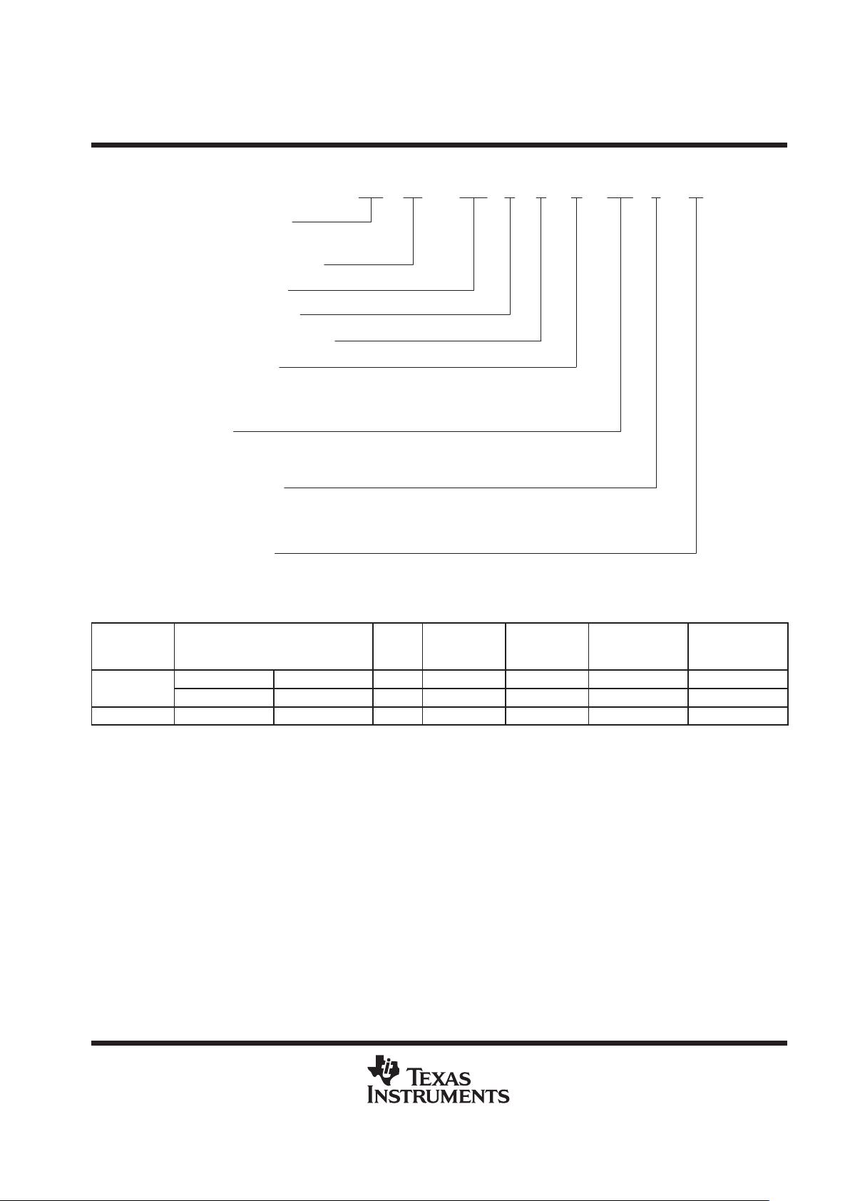
functional block diagram
The following terminals have 10-kΩ pullup resistors added within the module:
D CREQx_C40_#1, CACKx_C40_#1, CSTRBx_C40_#1, CRDYx_C40_#1, where x = 1, 2, 3, 4, or 5
D CREQy_C40_#2, CACKy_C40_#2, CSTRBy_C40_#2, CRDYy_C40_#2, where y = 0, 1, 2, 4, or 5
D LCE1_C40_#1, LCE2_C40_#2 (internal connections)
A total of 18 decoupling capacitors have been connected within the module.
Between clean power and ground, the following capacitors have been connected:
D Two 0.1-µF capacitors
D Two 0.01-µF capacitors
Between dirty power and ground, the following capacitors have been connected:
D Twelve 0.1-µF capacitors
D Two 0.01-µF capacitors
Page 7

SMJ320MCM42C, SMJ320MCM42D
DUAL SMJ320C40 MULTICHIP MODULE
SGKS001B – JULY 1997 – REVISED FEBRUARY 2000
7
POST OFFICE BOX 1443 • HOUSTON, TEXAS 77251–1443
functional block diagram (continued)
TDI_C40_#1
TCK_COMM
TMS_COMM
TRST_COMM
EMU0_COMM
EMU1_COMM
TDO_C40_#2
D31–D0
A30–A0
AE
DE
STAT3 –STAT0
LOCK
STRB0–STRB1
R/W0–R/W1
PAGE0–PAGE1
RDY0
–RDY1
CE0–CE1
TCLK0–TCLK1
NMI
IACKH1H3
IIOF3–IIOF0
RESETLOC0-
ROMEN
CREQ
CACK
CSTRB
CRDY
CD7–CD0
TDI
TDO
COMM0
COMM3
’C40_#1
ADDR
DATA
CNTL
ADDR
DATA
CNTL
’C40_ #2
TDI
TDO
CLKIN_COMM
RESET_COMM
VSS_CL
VCC_CL
VSS_DR
VCC_DR
SRAM
128K × 8 ×4
(’42D)
or
128K × 8 × 8
(’42C)
SRAM
128K × 8 ×4
(’42D)
or
128K × 8 × 8
(’42C)
D31–D0
A30–A0
AE
DE
STAT3 –STAT0
LOCK
STRB0–STRB1
R/W0–R/W1
PAGE0–PAGE1
RDY0
–RDY1
CE0–CE1
TCLK0–TCLK1
NMI
IACK
H1
H3
IIOF3–IIOF0
RESETLOC0–
ROMEN
CREQ
CACK
CSTRB
CRDY
CD7–CD0
’C40_ #2
Global Bus
IEEE 1149.1
’C40_ #1
Global Bus
’C40_ #2
Control
Communication Ports
(0–2, 4–5)
Communication Ports
(1–5)
’C40_#1
Control
’C40_#1
’C40_#2
RESETLOC1
RESETLOC1
Local Bus Local Bus
Page 8

SMJ320MCM42C, SMJ320MCM42D
DUAL SMJ320C40 MULTICHIP MODULE
SGKS001B – JULY 1997 – REVISED FEBRUARY 2000
8
POST OFFICE BOX 1443 • HOUSTON, TEXAS 77251–1443
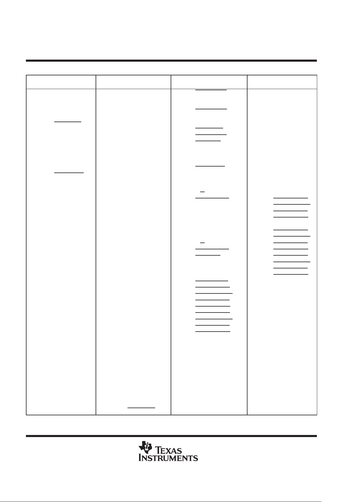
operational overview
Treatment of the detailed operation of the ’C40 device is not included in the scope of this document. See the
TMS320C4x User’s Guide
(literature number SPRU063) for a detailed description of this DSP . See Figure 1 and
Figure 2 for the memory map.
000000000h
000000FFFh
000001000h
0000FFFFFh
000100000h
0001000FFh
000100100h
0001FFFFFh
000200000h
0002FF7FFh
0002FF800h
0002FFBFFh
0002FFC00h
0002FFFFFh
000300000h
0007FFFFFh
000800000h
00081FFFFh
000820000h
07FFFFFFFh
080000000h
0FFFFFFFFh
Reserved
Peripherals (internal)
Reserved
Reserved
1K RAM BLK 0 (internal)
1K RAM BLK 1 (internal)
Reserved
Local Bus Module RAM
Reserved
Global Bus (external)
(a) INTERNAL ROM DISABLED
(ROMEN = 0)
Reserved
Peripherals (internal)
Reserved
Reserved
1K RAM BLK 0 (internal)
1K RAM BLK 1 (internal)
Reserved
Local Bus Module RAM
Reserved
Global Bus (external)
(b) INTERNAL ROM ENABLED
(ROMEN = 1)
1M
4K ROM (reserved)
1M
1M
5M
128K
Structure
Depends On
ROMEN Bit
Structure
Identical
2G
2G
Figure 1. Memory Map for Each ’C40 Within the Multichip Module (’42D)
Page 9

SMJ320MCM42C, SMJ320MCM42D
DUAL SMJ320C40 MULTICHIP MODULE
SGKS001B – JULY 1997 – REVISED FEBRUARY 2000
9
POST OFFICE BOX 1443 • HOUSTON, TEXAS 77251–1443
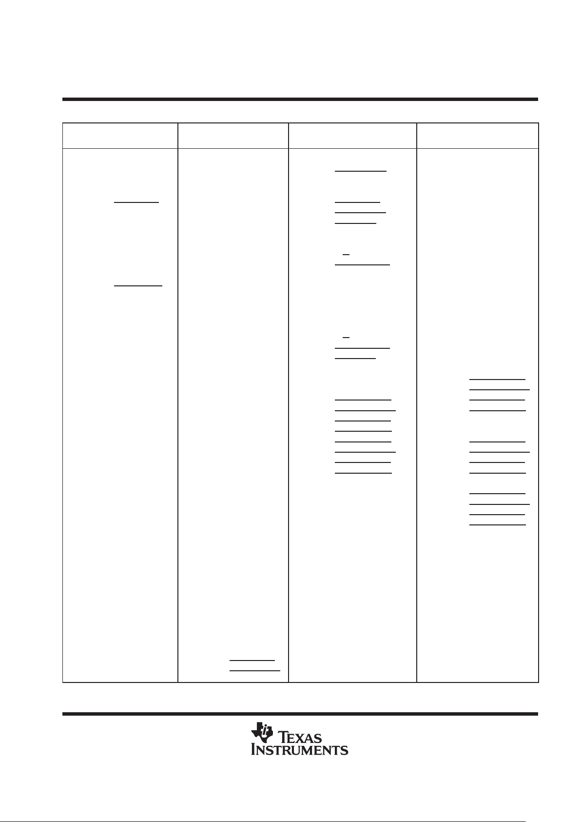
operational overview (continued)
000000000h
000000FFFh
000001000h
0000FFFFFh
000100000h
0001000FFh
000100100h
0001FFFFFh
000200000h
0002FF7FFh
0002FF800h
0002FFBFFh
0002FFC00h
0002FFFFFh
000300000h
000FDFFFFh
000FE0000h
000FFFFFFh
001000000h
00101FFFFh
001020000h
07FFFFFFFh
080000000h
0FFFFFFFFh
Reserved
Peripherals (internal)
Reserved
Reserved
1K RAM BLK 0 (internal)
1K RAM BLK 1 (internal)
Reserved
Local Bus Module RAM
(LSTRB0)
†
Reserved
Global Bus (external)
(a) INTERNAL ROM DISABLED
(ROMEN = 0)
Reserved
Peripherals (internal)
Reserved
Reserved
1K RAM BLK 0 (internal)
1K RAM BLK 1 (internal)
Reserved
Local Bus Module RAM
(LSTRB0)
†
Reserved
Global Bus (external)
(b) INTERNAL ROM ENABLED
(ROMEN = 1)
1M
4K ROM (reserved)
1M
1M
5M
128K
Structure
Depends On
ROMEN Bit
Structure
Identical
Local Bus Module RAM
(LSTRB1)
†
Local Bus Module RAM
(LSTRB1)
†
128K
256K
2G
2G
†
See section titled ”application note”.
Figure 2. Memory Map for Each ’C40 Within the Multichip Module (’42C)
Page 10

SMJ320MCM42C, SMJ320MCM42D
DUAL SMJ320C40 MULTICHIP MODULE
SGKS001B – JULY 1997 – REVISED FEBRUARY 2000
10
POST OFFICE BOX 1443 • HOUSTON, TEXAS 77251–1443
application note
For the ’MCM42C, the location of the local memory has changed from that of the ’MCM42D. In addition, to make
proper use of the local memory, it is necessary to understand how it is controlled.
In the case of the ’MCM42C, the lower 128K of memory is controlled by LSTRB0, while the upper 128K of
memory is controlled by LSTRB1. Since the upper 128K begins at address 1000000h, it is necessary to load
the value 101 1 1 (binary) into the STRB ACTIVE area (bits 28–24) of the local memory interface control register
(LMICR). This process ensures that the ’C40 uses LSTRB0
to control the lower 128K and LSTRB1 to control
the upper 128K.
In the case of the ’MCM42D, LSTRB0 controls the entire 128K. The value loaded into the STRB ACTIVE area
of the LMICR after reset is sufficient to control the memory . This value is 1 110, and tells the ’C40 that the entire
local memory is controlled by LSTRB0.
This subject is discussed in depth in Chapter 9 of the
1996 TMS320C4x User’s Guide
(literature number
SPRU063). In particular, section 9.3 discusses the proper use of the memory interface control registers.
reference documentation and data sheet scope
The SMJ320MCM42 is qualified to MIL-PRF-38535. Electrical continuity of the module is ensured through the
use of IEEE-1149.1-compatible boundary-scan testing and functional checkout of the local SRAM space.
KGD refers to TI known-good-die strategy. TI KGDs are fully tested over the military temperature range per
MIL-PRF-38535 QML. Electrical tests ensure compliance of the ’C40 KGD components to the SMJ320C40 data
sheet (literature number SGUS017) over the operating temperature range. Module timings are virtually
unchanged from the SMJ320C40 data sheet timings. An SMJ320C40 data sheet is provided for customer
reference only and does not imply MCM compliance to published timings.
For a description of the ’C40 operation and application information, see the
TMS320C4x User’s Guide
(literature
number SPRU063).
Page 11

SMJ320MCM42C, SMJ320MCM42D
DUAL SMJ320C40 MULTICHIP MODULE
SGKS001B – JULY 1997 – REVISED FEBRUARY 2000
11
POST OFFICE BOX 1443 • HOUSTON, TEXAS 77251–1443
absolute maximum ratings over operating free-air temperature range (unless otherwise noted)
†
Supply voltage range, VCC (see Note 1) – 0.3 V to 7 V. . . . . . . . . . . . . . . . . . . . . . . . . . . . . . . . . . . . . . . . . . . . . .
Voltage range on any terminal – 0.3 V to 7 V. . . . . . . . . . . . . . . . . . . . . . . . . . . . . . . . . . . . . . . . . . . . . . . . . . . . . . .
Output voltage range, VO – 0.3 V to 7 V. . . . . . . . . . . . . . . . . . . . . . . . . . . . . . . . . . . . . . . . . . . . . . . . . . . . . . . . . . .
Operating free-air temperature range (commercial [L version]), TA 0°C to 70°C. . . . . . . . . . . . . . . . . . . . . . .
(military [M version]), TA – 55°C to 125°C. . . . . . . . . . . . . . . . . . . . . .
Junction temperature, T
J
150°C. . . . . . . . . . . . . . . . . . . . . . . . . . . . . . . . . . . . . . . . . . . . . . . . . . . . . . . . . . . . . . . . . .
Storage temperature range, T
stg
– 65°C to 150°C. . . . . . . . . . . . . . . . . . . . . . . . . . . . . . . . . . . . . . . . . . . . . . . . . .
†
Stresses beyond those listed under “absolute maximum ratings” may cause permanent damage to the device. These are stress ratings only, and
functional operation of the device at these or any other conditions beyond those indicated under “recommended operating conditions” is not
implied. Exposure to absolute-maximum-rated conditions for extended periods may affect device reliability.
NOTE 1: All voltage values are with respect to VSS.
recommended operating conditions
MIN MAX UNIT
’42-33 4.5 5.5
V
CC
Supply voltage
’42-40
4.75 5.25
V
CLKIN_COMM 2.6 VCC+ 0.3
V
IH
High-level input voltage
CSTRBx
, CRDYx, CREQx, CACKx 2.2 VCC+ 0.3
V
VIHHigh level in ut voltage
All others 2 VCC+ 0.3
V
V
IL
Low-level input voltage – 0.3 0.8 V
I
OH
High-level output current – 300 µA
I
OL
Low-level output current 2 mA
p
p
L version 0 70
°
T
A
Operating free-air temperature range
M version – 55 125
°C
electrical characteristics over recommended ranges of supply voltage and operating free-air
temperature (see Note 2)
PARAMETER TEST CONDITIONS
†
MIN TYP MAX UNIT
V
OH
High-level output voltage VCC = MIN, IOH = MAX 2.4 3 V
V
OL
Low-level output voltage VCC = MIN, IOL = MAX 0.3 0.6 V
’42D
0.7 1.1
I
CC
Supply current
’42C
VCC = MAX
0.8 1.5
A
I
Z
3-state current VI = VSS to V
CC
– 20 20 µA
I
I
Input current VI = VSS to V
CC
– 10 10 µA
I
I2
Input current, COMM signal (see Note 3) VI = VSS to V
CC
– 20 20 µA
I
IP
Input current, internal pullup (see Note 4) VI = VSS to V
CC
– 400 30 µA
I
IP2
Input current, dual internal pullup (see Note 5) VI = VSS to V
CC
– 800 60 µA
I
IC
Input current, CLKIN_COMM VI = VSS to V
CC
– 60 60 µA
†
For conditions shown as MIN/MAX, use the appropriate value specified under recommended operating conditions.
NOTES: 2. Electrical characteristics are calculated algebraically from the SMJ320C40 data sheet limits.
3. Includes signals EMU0_COMM, EMU1_COMM, and RESET_COMM
4. Applies to TDI_C40_#1
5. Includes signals TCK_COMM, TMS_COMM, and TRST_COMM
Page 12

SMJ320MCM42C, SMJ320MCM42D
DUAL SMJ320C40 MULTICHIP MODULE
SGKS001B – JULY 1997 – REVISED FEBRUARY 2000
12
POST OFFICE BOX 1443 • HOUSTON, TEXAS 77251–1443
capacitance
Capacitance of a ’C40 die is specified by design to be 15 pF maximum for both inputs and outputs. Module
networks add up to 5 pF. Characterization of die or substance capacitance is performed after any design
change. Power measurements taken for a ’C40 die are made with an additional 80-pF load capacitance. Refer
to the SMJ320C40 data sheet (literature number SGUS017) for the test load circuit.
operational timings and module testing
Texas Instruments processing assures that operation is verified to published data sheet specifications on the
’C40 in die form. All voltage, timing, speed, and temperature specifications are met before any die is placed into
a multichip module. For this reason, all ’C40 voltage and timing parameters at the module level need not be
verified.
Characterization of the ’42 substrate shows that the module performs as an equivalent system of discretely
packaged ’C40 devices. This performance is assured through a full-frequency functional checkout of the module
that verifies selected worst-case timings. An additional propagation delay is introduced by the substrate. This
value is assured by design to be less than 1 ns, but it is not tested. See the SMJ320C40 data sheet (literature
number SGUS017) for a complete listing of timing diagrams and limits.
module test capability (future compatibility)
The ’C40 supports the IEEE-1149.1 testability standard, and the test access port (TAP) is brought out to the
module footprint. TDI is connected to ’C40_#1, TDO of ’C40_#1 is connected to TDI of ’C40_#2, and TDO of
’C40_#2 is brought out to the T AP. TCK_COMM, TMS_COMM, and TRST_COMM
are routed to both ’C40s in
the module. This configuration allows users to test the module using third-party JT AG testability tools or other
boundary-scan control software. Proper software configuration allows users to debug or launch code on the
module by way of the ’C40 emulator and extended development system (XDS) pod. Both of these tools are
used as part of outgoing module testing.
The ’42 supports third-party JT AG diagnostic families of products for verification and debug of boundary-scan
circuits, boards, and systems. Further information on JTAG testability tools is available through any TI sales
representative or authorized TI distributor.
XDS is a trademark of Texas Instruments Incorporated.
Page 13

SMJ320MCM42C, SMJ320MCM42D
DUAL SMJ320C40 MULTICHIP MODULE
SGKS001B – JULY 1997 – REVISED FEBRUARY 2000
13
POST OFFICE BOX 1443 • HOUSTON, TEXAS 77251–1443
module test circuit
Figure 3 illustrates the basic circuits for the ’42. See the
TMS320C4x User’s Guide
(literature number
SPRU063) for more detailed information.
TDI TDO
’C40_#1
TDI TDO
’C40_#2
TDO_C40_#2
TMS_COMM
TCK_COMM
TRST_COMM
EMU0_COMM
EMU1_COMM
TDI_C40_#1
5 V
CLKIN_COMM = Clock Pulse as shown in the Data Sheet
RESET_COMM
= Reset Pulse as shown in the Data Sheet
Test Header
†
SMJ320MCM42
All VCC to 5 V
All VSS to GND
4.7 kΩ–10 kΩ
Suggested
†
The test header normally consists of the XDS510 for the ’C40 emulation or ASSET hardware for interconnect testing.
Figure 3. Sample Test Circuit
XDS510 is a trademark of Texas Instruments Incorporated.
Page 14

SMJ320MCM42C, SMJ320MCM42D
DUAL SMJ320C40 MULTICHIP MODULE
SGKS001B – JULY 1997 – REVISED FEBRUARY 2000
14
POST OFFICE BOX 1443 • HOUSTON, TEXAS 77251–1443
thermal analysis
Thermal conduction of components in the SMJ320MCM42 is dependent on thermal resistance of the material
under each die as well as die area thermally connected to the heat-dissipating medium. Since these properties
vary with layout and die size, ’C40 and SRAM components should be considered separately. Table 2 lists
primary parameters required for thermal analysis of the module. T
J
, the maximum junction temperature, is not
to be exceeded for the ’C40s or the SRAM die.
T able 2. Thermal Characteristics
PARAMETER MIN TYP MAX UNIT
T
J
Maximum allowable junction temperature under operating condition 150 °C
P
MCM
Module power dissipation 3.5 5.8 W
T
JC_pkg
†
Average thermal impedance (junction to case) for the package 2.1 °C/W
T
JA
Thermal impedance (junction to ambient air, 0 cfm) of package 20.5 °C/W
T
SOL
Maximum solder temperature (10 s duration) 260 °C
†
TJC package data was taken under the following conditions: two ’C40s dissipating 1.05 W each and eight SRAMs dissipating 0.175 W each.
power estimation
During the operation verification, the power requirements of the SMJ320MCM42 are characterized over the
operating free-air temperature range. See the application report
Calculation of TMS320C40 Power Dissipation
(literature number SPRA032) as reference for power estimation of the ’C40 components.
Typical power dissipation is measured with both ’C40s executing a 64-point fast Fourier transform (FFT)
algorithm. Input and output data arrays reside in module SRAM, and output data is written out to the
global-address space. The global databus is loaded with 80-pF test loads, and both local and global writes are
configured for zero-wait-state memory. Under typical conditions of 25°C, 5-V VCC, and 40-MHz CLKIN
frequency, the power dissipation is measured to be 3.5 W.
Maximum power dissipation is measured under worst-case conditions. The global databus is loaded with 80-pF
test loads, and simultaneous zero-wait-state writes are performed to both local and global buses. Under
worst-case environment conditions of – 55°C, 5.25-V V
CC
, and 40-MHz CLKIN frequency , the power dissipation
is determined to be 5.9 W. The algorithm executed during these tests consists of parallel writes of alternating
0xAAs and 0x55s to both local SRAM and global-address spaces. This algorithm is not considered to be a
practical use of the ’C40’s resources; therefore, the associated power measurement must be considered
absolute maximum only.
Page 15

SMJ320MCM42C, SMJ320MCM42D
DUAL SMJ320C40 MULTICHIP MODULE
SGKS001B – JULY 1997 – REVISED FEBRUARY 2000
15
POST OFFICE BOX 1443 • HOUSTON, TEXAS 77251–1443
MECHANICAL DATA
HFN (S-CQFP-F408) CERAMIC QUAD FLATPACK WITH TIE-BAR
0.225 (5,72)
0.175 (4,45)
408
2.810 (71,37)
2.820 (71,73)
307
4.050 (102,87)
”B”
DETAIL ”B”
0.012 (0,30)
0.006 (0,15)
0.095 (2,41)
0.070 (1,78)
0.140 (3,56)
0.175 (4,45)
4073431/B 10/98
3.850 (97,79) TYP
SQ
1
102
2.626 (66,70)
2.525 (64,13) TYP
2.674 (67,92)
”A”
103
204
306
0.012 (0,30)
0.007 (0,18)
205
DETAIL ”A”
0.020 (0,51) MAX
0.005 (0,13)
0.009 (0,23)
0.025 (0,65)
NOTES: A. All linear dimensions are in inches (millimeters).
B. This drawing is subject to change without notice.
Page 16

IMPORTANT NOTICE
T exas Instruments and its subsidiaries (TI) reserve the right to make changes to their products or to discontinue
any product or service without notice, and advise customers to obtain the latest version of relevant information
to verify, before placing orders, that information being relied on is current and complete. All products are sold
subject to the terms and conditions of sale supplied at the time of order acknowledgement, including those
pertaining to warranty, patent infringement, and limitation of liability.
TI warrants performance of its semiconductor products to the specifications applicable at the time of sale in
accordance with TI’s standard warranty. Testing and other quality control techniques are utilized to the extent
TI deems necessary to support this warranty. Specific testing of all parameters of each device is not necessarily
performed, except those mandated by government requirements.
CERT AIN APPLICATIONS USING SEMICONDUCTOR PRODUCTS MAY INVOLVE POTENTIAL RISKS OF
DEATH, PERSONAL INJURY, OR SEVERE PROPERTY OR ENVIRONMENTAL DAMAGE (“CRITICAL
APPLICATIONS”). TI SEMICONDUCTOR PRODUCTS ARE NOT DESIGNED, AUTHORIZED, OR
WARRANTED TO BE SUITABLE FOR USE IN LIFE-SUPPORT DEVICES OR SYSTEMS OR OTHER
CRITICAL APPLICATIONS. INCLUSION OF TI PRODUCTS IN SUCH APPLICA TIONS IS UNDERSTOOD T O
BE FULLY AT THE CUSTOMER’S RISK.
In order to minimize risks associated with the customer’s applications, adequate design and operating
safeguards must be provided by the customer to minimize inherent or procedural hazards.
TI assumes no liability for applications assistance or customer product design. TI does not warrant or represent
that any license, either express or implied, is granted under any patent right, copyright, mask work right, or other
intellectual property right of TI covering or relating to any combination, machine, or process in which such
semiconductor products or services might be or are used. TI’s publication of information regarding any third
party’s products or services does not constitute TI’s approval, warranty or endorsement thereof.
Copyright 2000, Texas Instruments Incorporated
 Loading...