

Page 1
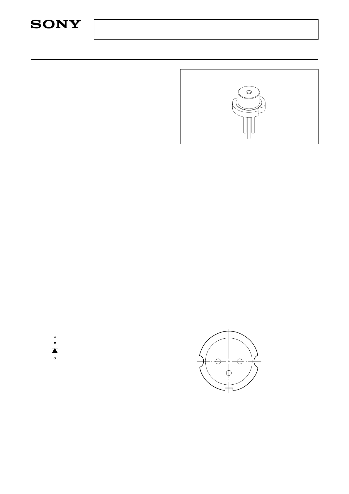
SLD237VL
For the availability of this product, please contact the sales office.
Index-Guided High Power AlGaAs Laser Diode
Description
The SLD237VL is a high-power , index-guided AlGaAs
laser diode.
Features
• High power
• Low current consumption
• Small astigmatism
• Small package (φ5.6mm)
Applications
Optical pickup for CD-R/RW
Structure
AlGaAs quantum well structured laser diode
M-274
Recommended Operating Optical Power Output 80mW
Absolute Maximum Ratings
• Optical power output Pomax 90 mW (CW)
130 mW (Pulse)
Pulse width 200ns or less
Duty 50% or less
• Reverse voltage VR LD 2 V
• Operating temperature Topr –10 to +70 °C
• Storage temperature Tstg –40 to +85 °C
Connection Diagram Pin Configuration
COMMON
3
LD
1
(Pulse Operation)
2
3
Bottom View
1
1. LD anode
2. N.C.
3. COMMON
Sony reserves the right to change products and specifications without prior notice. This information does not convery any license by
any implication or otherwise under any patents or other right. Application circuits shown, if any, are typical examples illustrating the
operation of the devices. Sony cannot assume responsibility for any problems arising out of the use of these circuits.
– 1 –
E00852B19-PS
Page 2

SLD237VL
Optical and Electrical Characteristics (Tc = 25°C) Tc: Case temperature
Item
Threshold current
Operating current
Operating voltage
Wavelength
Differential efficiency
Radiation
angle
Paralell
Perpendicular
Astigmatism
Positional
Angle
accuracy
Position
Symbol
Ith
Iop
Vop
λp
ηD
θ//
θ⊥
As
∆φ//
∆φ⊥
∆X, ∆Y, ∆Z
Conditions
CW
CW, Po = 80mW
CW, Po = 80mW
CW, Po = 80mW
CW, Po = 80mW
CW, Po = 80mW
CW, Po = 80mW
CW, Po = 80mW
CW, Po = 80mW
CW, Po = 80mW
Min.
25
90
—
779
0.7
7.4
15.0
–6
—
—
—
Typ.
30
110
2.0
784
1.0
8.3
18.0
—
—
—
—
Max.
40
130
2.3
789
1.3
9.5
21.0
0
±1.6
±2.5
±80
Unit
mA
mA
V
nm
mW/mA
deg
deg
µm
deg
deg
µm
– 2 –
Page 3
SLD237VL
Notes on Operation
Care should be taken for the following points when using this product.
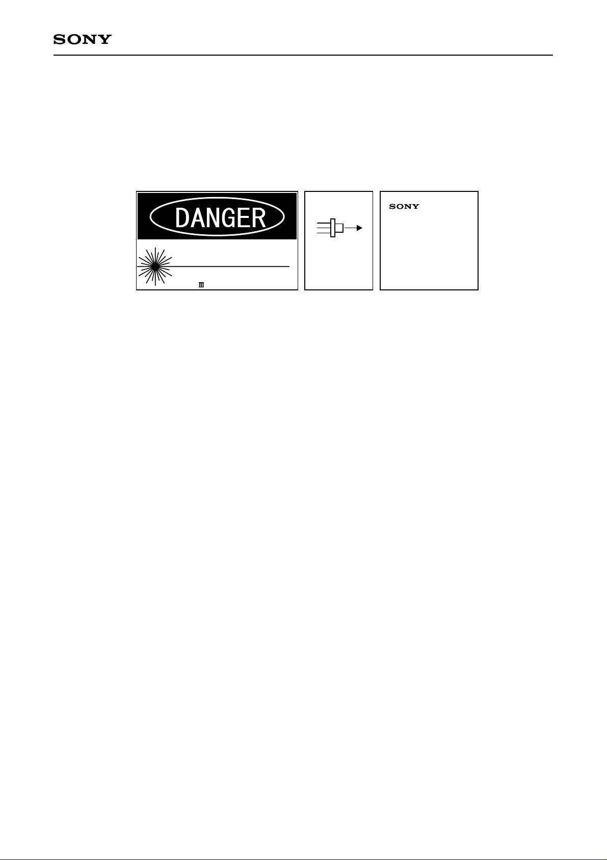
(1) This product corresponds to a Class 3B product under IEC60825-1 and JIS standard C6802 "Laser Product
Emission Safety Standards".
LASER RADIATION
AVOID DIRECT EXPOSURE TO BEAM
MAXIMUM OUTPUT 350 mW
WAVELENGTH 600 - 950 nm
CLASS III b LASER PRODUCT
LASER DIODE
AVOID EXPOSURE
Laser radiation is
emitted from this
aperture.
This product complies with 21
CFR Part 1040.10 and 1040.11
Sony Corporation
6-7-35 Kitashinagawa,
Shinagawa-ku,Tokyo
141-0001 Japan
LASER DIODE
(2) Eye protection against laser beams
Take care not to allow laser beams to enter your eyes under any circumstances.
For observing laser beams, ALWAYS use safety goggles that block laser beams. Usage of IR scopes, IR
cameras and fluorescent plates is also recommended for monitoring laser beams safely.
(3) Gallium Arsenide
This product uses gallium arsenide (GaAs). This is not a problem for normal use, but GaAs vapors may be
potentially hazardous to the human body. Therefore, never crush, heat to the maximum storage temperature
or higher, or place the product in your mouth.
In addition, the following disposal methods are recommended when disposing of this product.
1. Engaging the services of a contractor certified in the collection, transport and intermediate treatment
of items containing arsenic.
2. Managing the product through to final disposal as specially managed industrial waste which is
handled separately from general industrial waste and household waste.
(4) Prevention of surge current and electrostatic discharge
Laser diodes are most sensitive to electrostatic discharge among semiconductors. When a large current is
passed through the laser diode for even an extremely short time, the strong light emitted from the laser
diode promotes deterioration and then destruction of the laser diode. Therefore, note that surge current
should not flow to the laser diode driving circuit from switches and others. Also, if the laser diode is handled
carelessly, it may be destroyed instantly because electrostatic discharge is easily applied by a human body.
Therefore, be extremely careful about overcurrent and electrostatic discharge.
(5) Use for special applications
This product is not designed or manufactured for use in equipment used under circumstances where
failure may pose a risk to life and limb, or result in significant material damage, etc.
Consult your Sony sales representative when investigating use for medical, vehicle, nuclear power control
or other special applications. Also, use the power supply that was designed not to exceed the optical power
output specified at the absolute maximum ratings.
– 3 –
Page 4
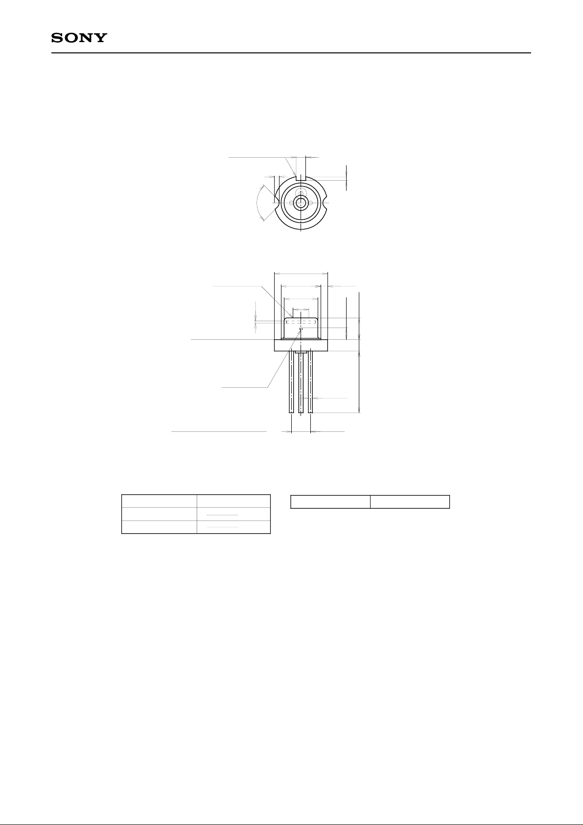
Package Outline Unit: mm
Reference
Slot
SLD237VL
M-274
1.0
Window Glass
Reference
Plane
LD Chip
& Photo
Diode
∗Optical
Distance = 1.35 ± 0.08
90˚
0.25
0.5
3
2
0
φ5.6 – 0.025
φ4.4 MAX
φ3.7 MAX
φ1.0 MIN
231
1
3 – φ0.45
PCD φ2.0
0.4
0.5 MIN
∗1.26
2.6 MAX
1.2 ± 0.1
6.5
SONY CODE
EIAJ CODE
JEDEC CODE
M-274
PACKAGE MASS
– 4 –
0.3g
Sony Corporation
 Loading...