

Page 1
TECHNICAL DATA
Semiconductor
SL74LV04
Hex Inverter
The SL74LV04 is a low -voltage Si-gate CMOS device that is pin and
function compatible with 74HC/HCT0 4A.
The SL74LV04 provides six inverting buffers.
• Wide Operating Voltage: 1.0 ~ 5.5 V
• Optimized for Low Voltage applications: 1.0 ~ 3.6 V
• Accepts TTL input levels between VCC =2.7 V and VCC =3.6 V
• Low Input Current
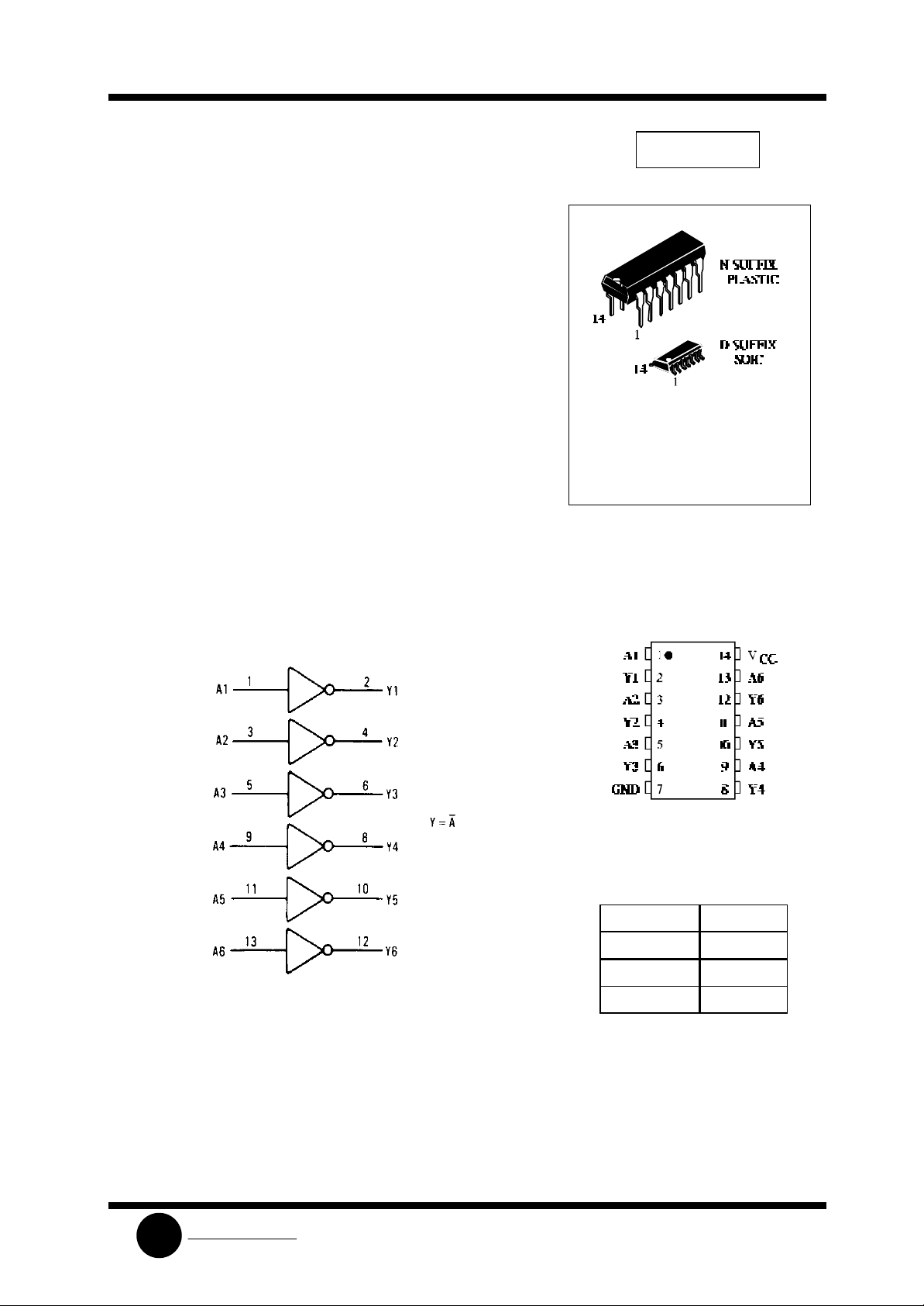
LOGIC DIAGRAM
ORDERING INFORMATION
SL74LV04N Plastic
SL74LV04D SOIC
SL74LV04 Chip
TA = -40° ÷ 125° C for all packages
PIN ASSIGNMENT
SLS
System Logic
PIN 14 =VCC
PIN 7 = GND
FUNCTION TABLE
Input Output
A Y
L H
H L
1
Page 2
SL74LV04
Semiconductor
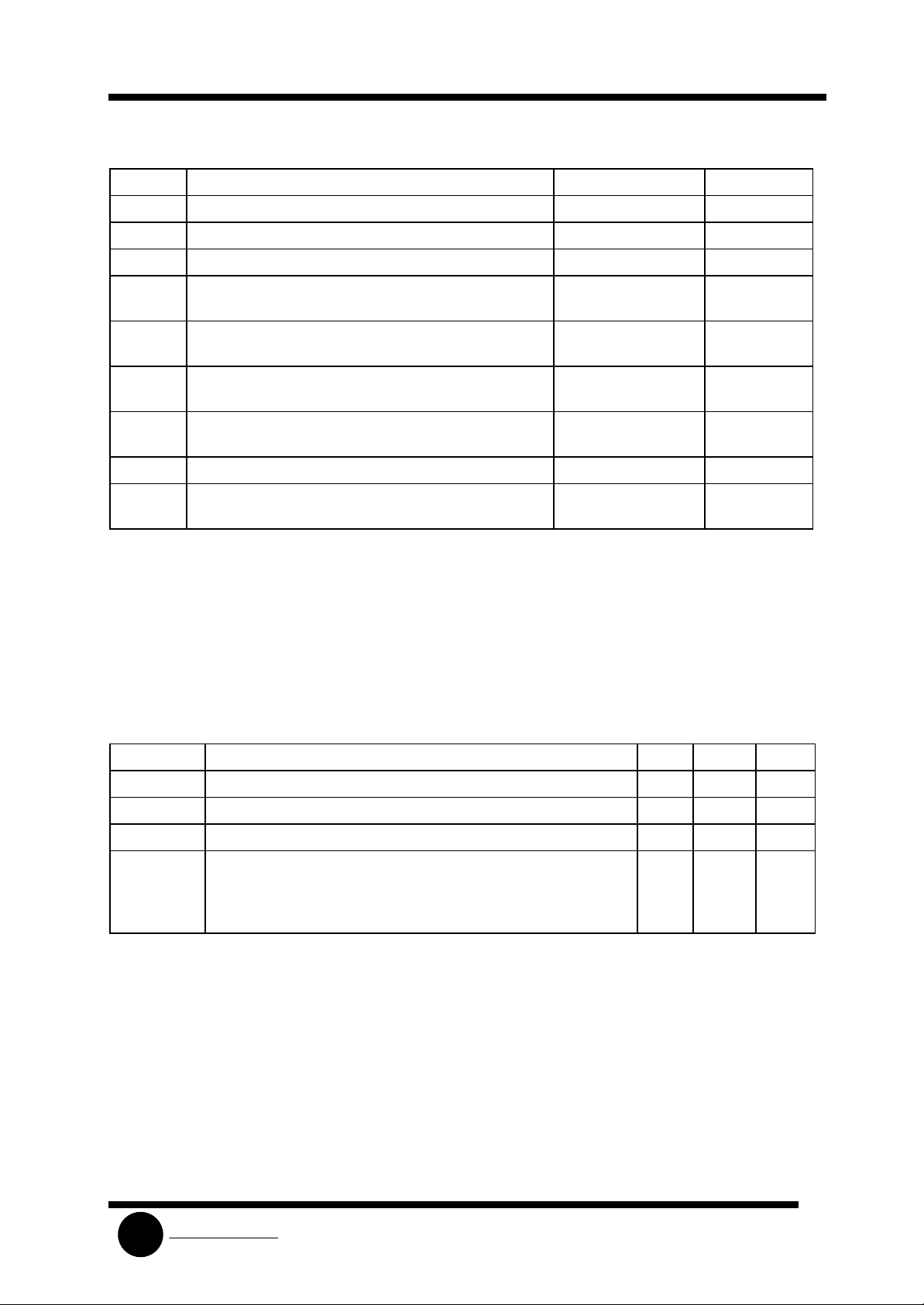
MAXIMUM RATINGS*
Symbol Parameter Value Unit
VCC DC supply voltage (Referenced to GND) -0.5 ~ +7.0 V
IIK*1 DC input diode current ±20 mA
IOK*2 DC output diode current ±50 m A
Io*3 DC output source or sink current
±25 mA
-bus driver outputs
I
DC GND current for types with
GND
±50 mA
- bus driver outputs
ICC DC VCC current for types with
±50 mA
- bus driver outputs
PD Power dissipation per package, plastic DIP+
SOIC package+
750
500
Tstg Storage temperature -65 ~ +150 °C
TL Lead temperature, 1.5 mm from Case for 10 seconds
260 °C
(Plastic DIP ), 0.3 mm (SOIC Package)
*
Maximum Ratings are those values beyond which damage to the device may occur.
Functional operation should be restricted to the Recommended Operating Conditions.
+Derating - Plastic DIP: - 12 mW/°C from 70° to 125°C
SOIC Package: : - 8 mW/°C from 70° to 125°C
*1: VI < -0.5V or V
> VCC+0.5V
I
*2: Vo < -0.5V or Vo > VCC+0.5V
*3: -0.5V < Vo < VCC+0.5V
RECOMMENDED OPERATING CONDITIONS
mW
Symbol Parameter Min Max Unit
VCC DC Supply Voltage (Referenced to GND) 1.0 5.5 V
VIN, V
DC Input Voltage, Output Voltage (Referenced to GND) 0 VCC V
OUT
TA Operating Temperature, All Package Types -40 +125 °C
tr, tf Input Rise and Fall Time VCC =1.2 V
VCC =2.0 V
V
=3.0 V
CC
V
=3.6 V
CC
0
0
0
0
1000
700
500
400
ns
This device contains protection circuitry to guard against damage due to high static voltages or electric
fields. However, precautions must be taken to avoid applications of any voltage higher than maximum rated
voltages to this high-impedance circuit. For proper operation, VIN and V
GND≤(VIN or V
OUT
)≤VCC.
should be constrained to the range
OUT
Unused inputs must always be tied to an appropriate logic voltage level (e.g., either GND or VCC). Unused
outputs must be left open.
SLS
System Logic
2
Page 3
Semiconductor
Level Output
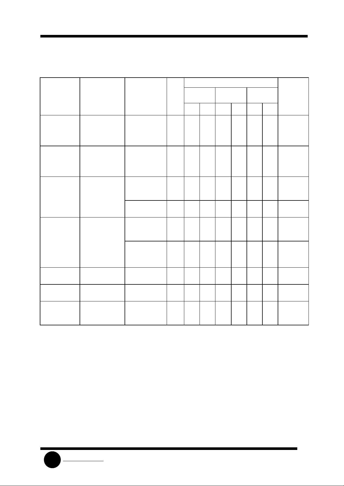
DC ELECTRICAL CHARACTERISTICS (Voltages Referenced to GND)
Guaranteed Limit
Symbol Parameter Test Conditions
VCC,
V
25°C -40°C ÷ 85°C -40°C ÷
min max min max min max
SL74LV04
125°C
Unit
VIH High-Level Input
Voltage
VIL Low-Level Input
Voltage
Voltage
VOL Low-Level Output
Voltage
VI = VIH or VIL
IIL Low-Level Input
Leakage Current
IIÍ High-Level Input
Leakage Current
IÑÑ Quiescent Supply
Current
(per Package)
1.2
1.2
VI = VIL
IO = -50 µA
VI = VIL
IO = -6.0 µA
VI = VIH
IO = 50 µA
IO = 6.0 m À
- -0.1 - -1.0 - -1.0
VI = VCC * - 0.1 - 1.0 - 1.0
VI = 0 Â or V
IO = 0 µA
CC
0.9
2.0
1.4
3.0
2.1
3.6
2.5
2.0
3.0
3.6
1.2
1.1
2.0
1.92
*
2.92
* 2.48 - 2.34 - 2.20 - V
1.2
2.0
3.0 - 0.33 - 0.4 - 0.5 V
* - 2.0 - 20 - 40
-
0.9
-
1.4
-
2.1
-
2.5
-
0.3
-
0.6
-
0.9
-
1.1
-
1.0
-
1.9
-
2.9
-
0.09
-
0.09
-
0.09
-
0.9
-
1.4
-
2.1
-
2.5
-
0.3
-
0.6
-
0.9
-
1.1
-
1.0
-
1.9
-
2.9
-
0.1
-
0.1
-
0.1
-
-
-
-
-
0.3
-
0.6
-
0.9
-
1.1
-
-
-
-
0.1
-
0.1
-
0.1
V
V
V VOH High-
V
µA
µA
µA
* : VCC= (3.3±0.3) V
System Logic
SLS
3
Page 4
SL74LV04
Semiconductor
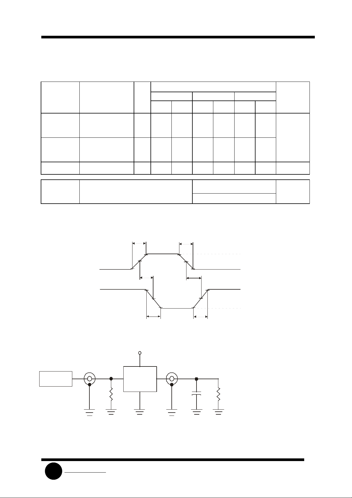
AC ELECTRICAL CHARACTERISTICS (C
VCC
V
=50 pF , tLH = tHL = 6.0 ns, VIL=0V, VIH=V
L
Guaranteed Limit
25°C -40°C ÷ 85°C -40°C ÷ 125°C Symbol Parameter
min max min max min max
t
t
THL,
PHL,
(t
(t
Output Transition
TLH)
Time, Any Output
(Figure 1)
Propagation Delay,
PLH)
Input A to Output Y
(Figure 1)
1.2
2.0
*
1.2
2.0
*
-
-
-
-
-
70
16
10
90
23
14
-
-
-
-
-
-
85
20
13
120
28
18
-
-
-
-
-
-
CI Input Capacitance 3.0 - - - 3.5 - 3.5 pF
ÒÀ=25°Ñ, VI=0V÷VCC CPD Power Dissipation Capacitance (Per Inverter)
42
Used to determine the no-load dynamic power consumption:
P
= CPDV
D
(CLV
2
fI+ (CLV
CC
2
fo) – sum of the outputs
CC
Input À
2
fo), fI - input frequency, fo - output frequency (MHz)
CC
t
HL
0.9
V
1
0.1
t
PHL
t
LH
V
0.9
V
1
0.1
t
PLH
CC
GND
100
24
15
150
34
21
CC, RL
=1 kÙ)
Unit
ns
pF
PULSE
GENERATOR
Output Y
V
0.9
V
1
t
TLH
V
GND
CC
V = 0.5 V
1 C C
0.9
t
THL
V
1
0.1 0.1
Figure 1. Switching Waveforms
V
CC
I
DEVICE
UNDER
R
TEST
T
V
O
C
L
Termination resistance RT – should
be equal to Z
of pulse
OUT
generators
R
L
Figure 2. Test Circui t
SLS
System Logic
4
Page 5
Semiconductor
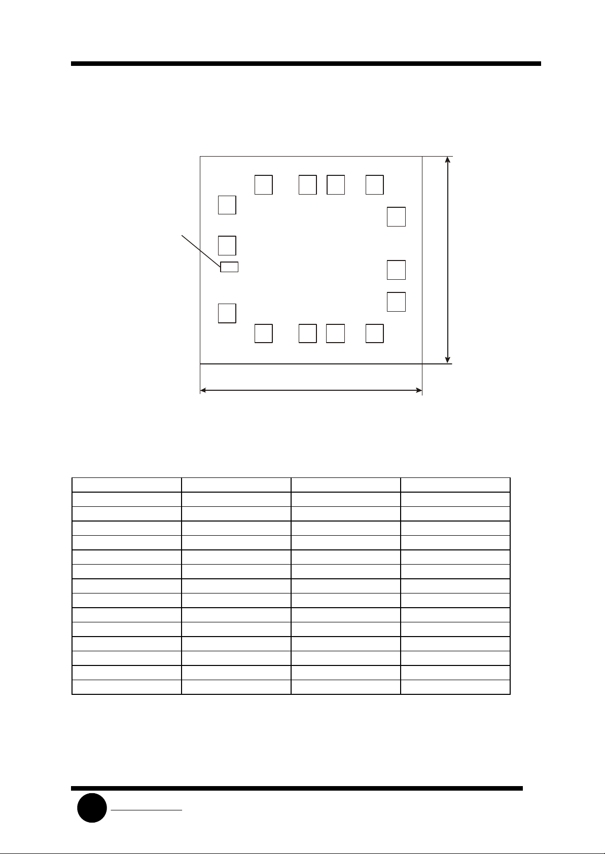
CHIP PAD DIAGRAM SL74LV04
SL74LV04
12
11
10
13
Chip marking
25LV04
(x=0.127; y=0.580
)
14
01
02
1.35 0.03
Pad size 0.108 x 0.108 mm (Pad size is given as per metallization layer)
Thickness of chip 0.46 ± 0,02 mm
03
±
04 05
PAD LOCATION
Pad No Symbol X Y
01 À1 0.111 0.228
02 Y1 0.333 0.111
03 A2 0.600 0.111
04 Y2 0.770 0.111
05 A3 1.006 0.111
06 Y3 1.138 0.293
07 GND 1.138 0.477
08 Y4 1.138 0.786
09 A4 1.006 0.970
10 Y5 0.771 0.970
11 A5 0.600 0.970
12 Y6 0.332 0.970
13 A6 0.111 0.855
14 Vcc 0.111 0.619
09
08
±
07
1.20 0.03
06
SLS
System Logic
5
 Loading...