

Page 1
Semiconductor
Octal 3-State Noninverting
Bus Transceiver
These octal bus transceiver are designed for asynchronous two way communication between data buses. The control function
implementation minimized external timing requirements.
The device allows data transmission from the A bus to the B bus or
from the B bus to the A bus depending upon the logic level at the
directional control (DIR) input. The enable input(E) can be used to
disable the device so that the buses are effectively isolated.
• Bidirectional Bus Transceiver in a High-Density 20-Pin Package
• 3-state Outputs Dirve Bus Lines Directly
• P-N-P Inputs D-C Loading on Bus Lines
• Hysteresis at Bus Inputs Improve Noise Margins
• Typical Propagation Delay Times; Port to Port ... 8 ns
SL74LS245
ORDERING INFORMATION
SL74LS245N Plastic
SL74LS245D SOIC
TA = 0° to 70° C
for all packages
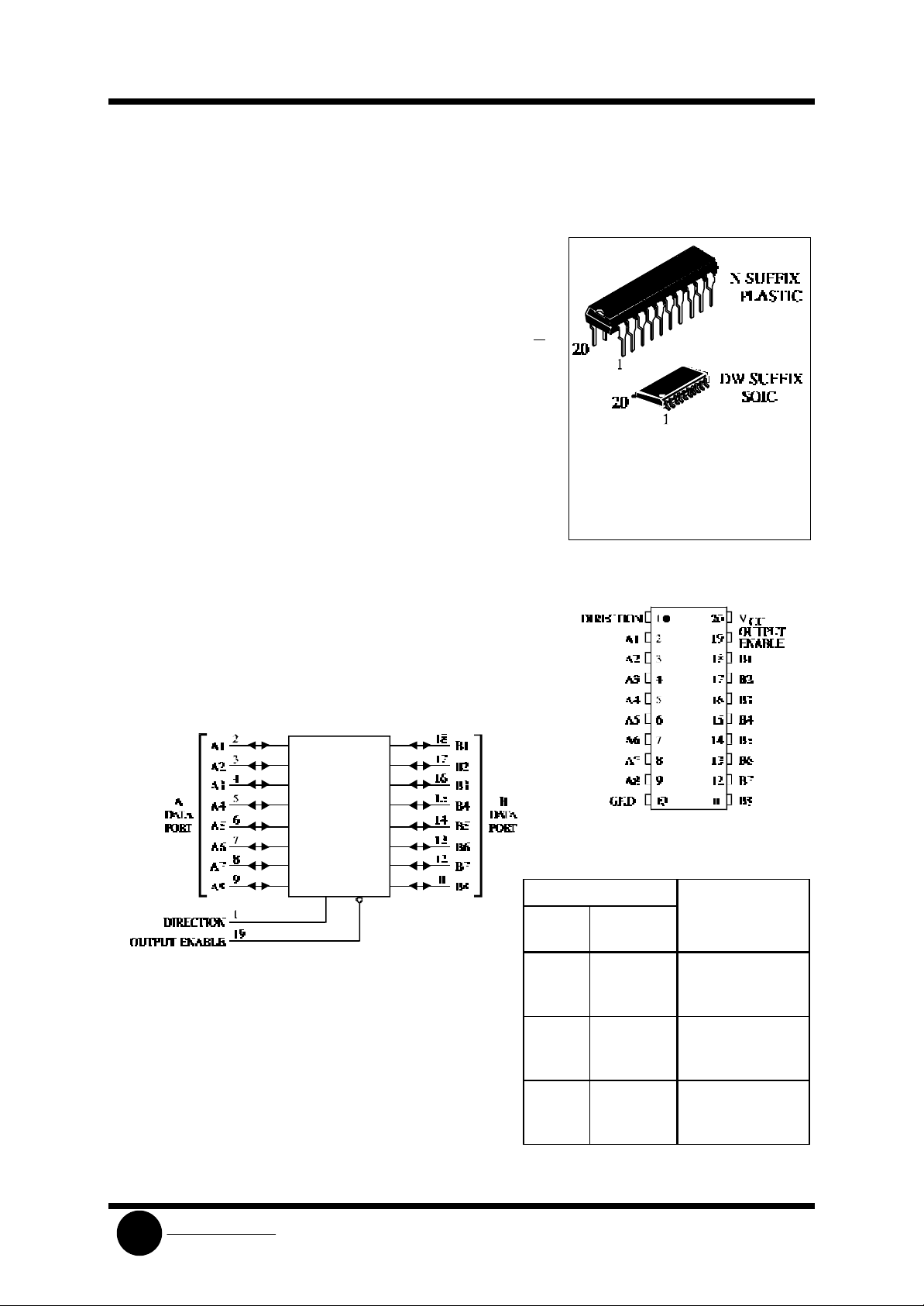
LOGIC DIAGRAM
PIN 20=VCC
PIN 10 = GND
PIN ASSIGNMENT
FUNCTION TABLE
Control Inputs
Output
Enable
L L Data Transmitted
L H Data Transmitted
Direction Operation
from Bus B to Bus
A
from Bus A to Bus
B
SLS
H X Buses Isolated
(High Impedance
State)
X = don’t care
System Logic
Page 2
SL74LS245
Semiconductor
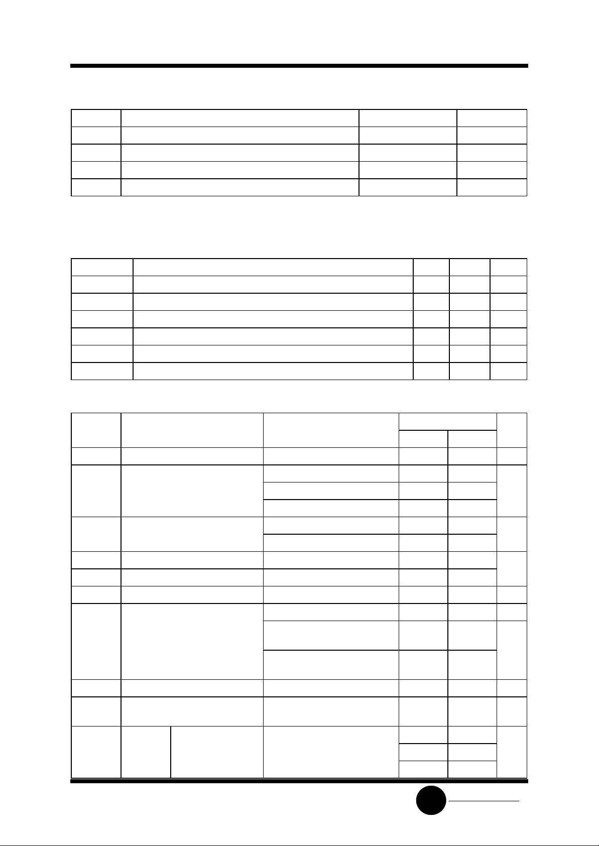
MAXIMUM RATINGS*
Symbol Parameter Value Unit
VCC Supply Voltage 7.0 V
VIN Input Voltage 7.0 V
V
Output Voltage 5.5 V
OUT
Tstg Storage Temperature Range -65 to +150 °C
*
Maximum Ratings are those values beyond which damage to the device may occur.
Functional operation should be restricted to the Recommended Operating Conditions.
RECOMMENDED OPERATING CONDITIONS
Symbol Parameter Min Max Unit
VCC Supply Voltage 4.75 5.25 V
VIH High Level Input Voltage 2.0 V
VIL Low Level Input Voltage 0.8 V
IOH High Level Output Current -15 mA
IOL Low Level Output Current 24 mA
TA Ambient Temperature Range 0 +70 °C
DC ELECTRICAL CHARACTERISTICS over full operating conditions
Guaranteed Limit
Symbol Parameter Test Conditions Min Max Unit
VIK Input Clamp Voltage VCC = min, IIN = -18 mA -1.5 V
VOH High Level Output Voltage VCC = min, IOH = -1.0 mA 2.7 V
VCC = min, IOH = -3.0 mA 2.4
VCC = min, IOH = -15 mA 2.0
VOL Low Level Output Voltage VCC = min, IOL = 12 mA 0.4 V
VCC = min, IOL = 24 mA 0.5
VT+ - VT- Hysteresis VCC = min 0.2 V
I
Output Off Current HIGH VCC = max, V
OZH
I
Output Off Current LOW VCC = max, V
OZL
IIH High Level Input Current VCC = max, VIN = 2.7 V 20 µA
VCC = max, VIN = 5.5 V
(A or B)
= 2.7 V 20 µA
OUT
= 0.4 V -0.2 mA
OUT
0.1 mA
VCC = max, VIN = 7.0 V
0.1
for Pin1, Pin 19
IIL Low Level Input Current VCC = max, VIN = 0.4 V -0.2 mA
IO Output Short Circuit Current VCC = max, VO =0 V
-40 -225 mA
(Note 1)
ICC Supply Outputs High VCC = max 70 mA
Current Outputs Low Outputs open 90
All outputs disable 95
System Logic
SLS
Page 3
SL74LS245
Semiconductor
Note 1: Not more thanone output should be shorted at a time, and duration of the short-circuit should not exceed
one second.
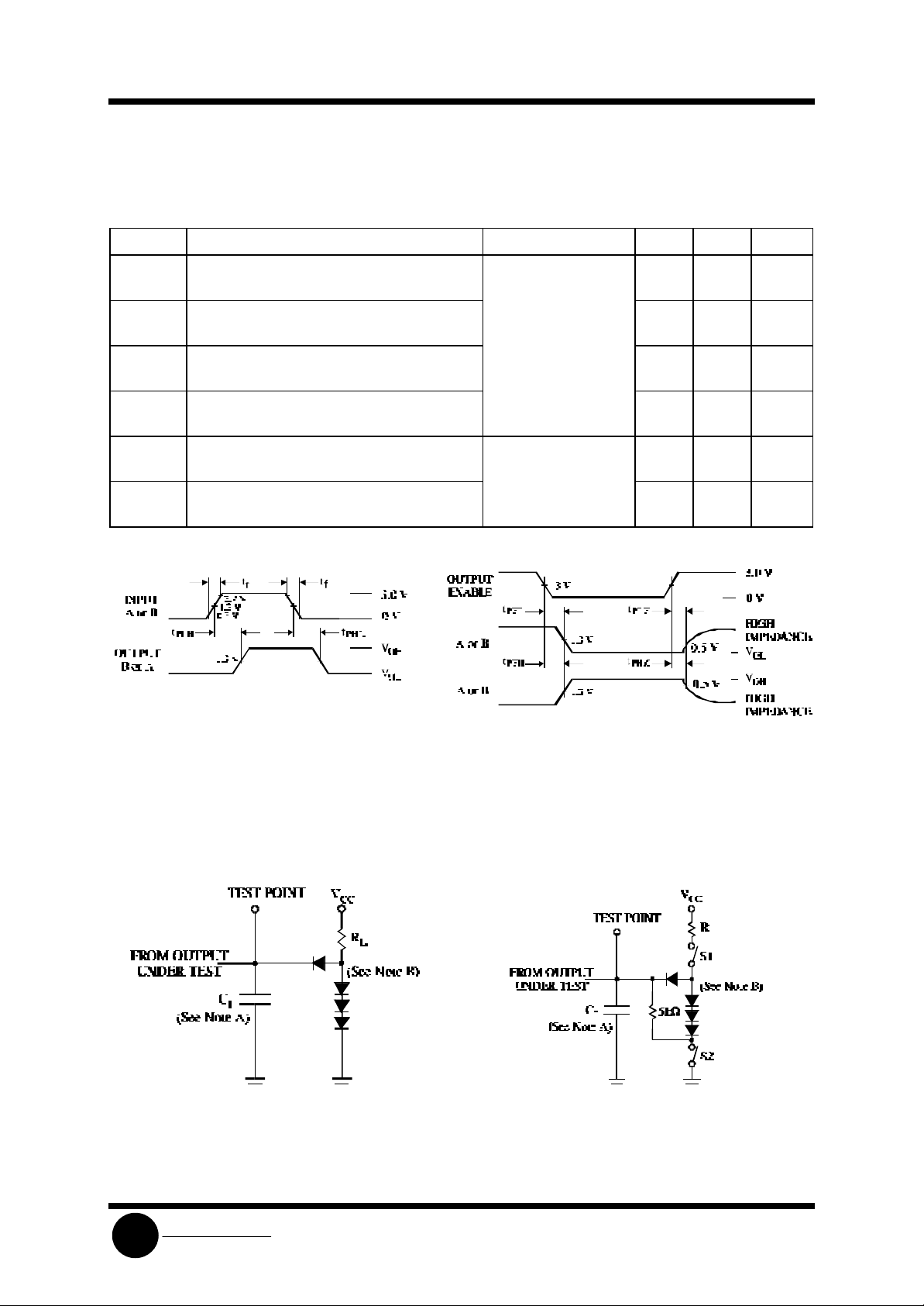
AC ELECTRICAL CHARACTERISTICS (T
tf = 6.0 ns)
Symbol Parameter Test Condition Min Max Unit
t
Propagation Delay Time, Low -to-High Level
PLH
Output (from A or B to Output)
t
Propagation Delay Time, High-to-Low Level
PHL
Output (from A or B to Output)
t
Output Enable Time to High Level (from OE
PZH
to Output)
t
Output Enable Time to Low Level (from OE
PZL
to Output)
t
Output Disable Time from High Level
PHZ
(from OE to Output)
t
Output Disable Time from Low Level
PLZ
(from OE to Output)
= 25°C, VCC = 5.0 V, tr = 15 ns,,
A
12 ns
CL = 45 pF,
12 ns
RL = 667 Ω
40 ns
40 ns
25 ns
CL = 5 pF
RL = 667 Ω 25 ns
t
Figure 1. Switching Waveforms
(See Figure 3)
NOTES A. CL includes probe and jig capacitance.
B. All diodes are 1N916 or 1N3064.
Figure 3. Test Circuit
- S1 closed, S2 opened
PZL
t
- S1 opened, S2 closed
PZH
t
, t
PLZ
- S1 and S2 closed
PHZ
Figure 2. Switching Waveforms
(See Figure 4)
NOTES A. CL includes probe and jig capacitance.
B. All diodes are 1N916 or 1N3064.
Figure 4. Test Circuit
SLS
System Logic
Page 4
SL74LS245
Semiconductor
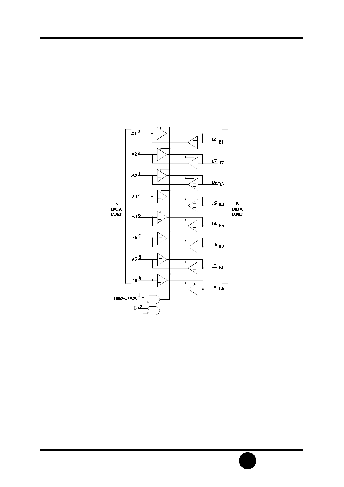
EXPANDED LOGIC DIAGRAM
SLS
System Logic
 Loading...