

Page 1
SL7101
S
EARTH LEAKAGE CURRENT DETECTOR
Description
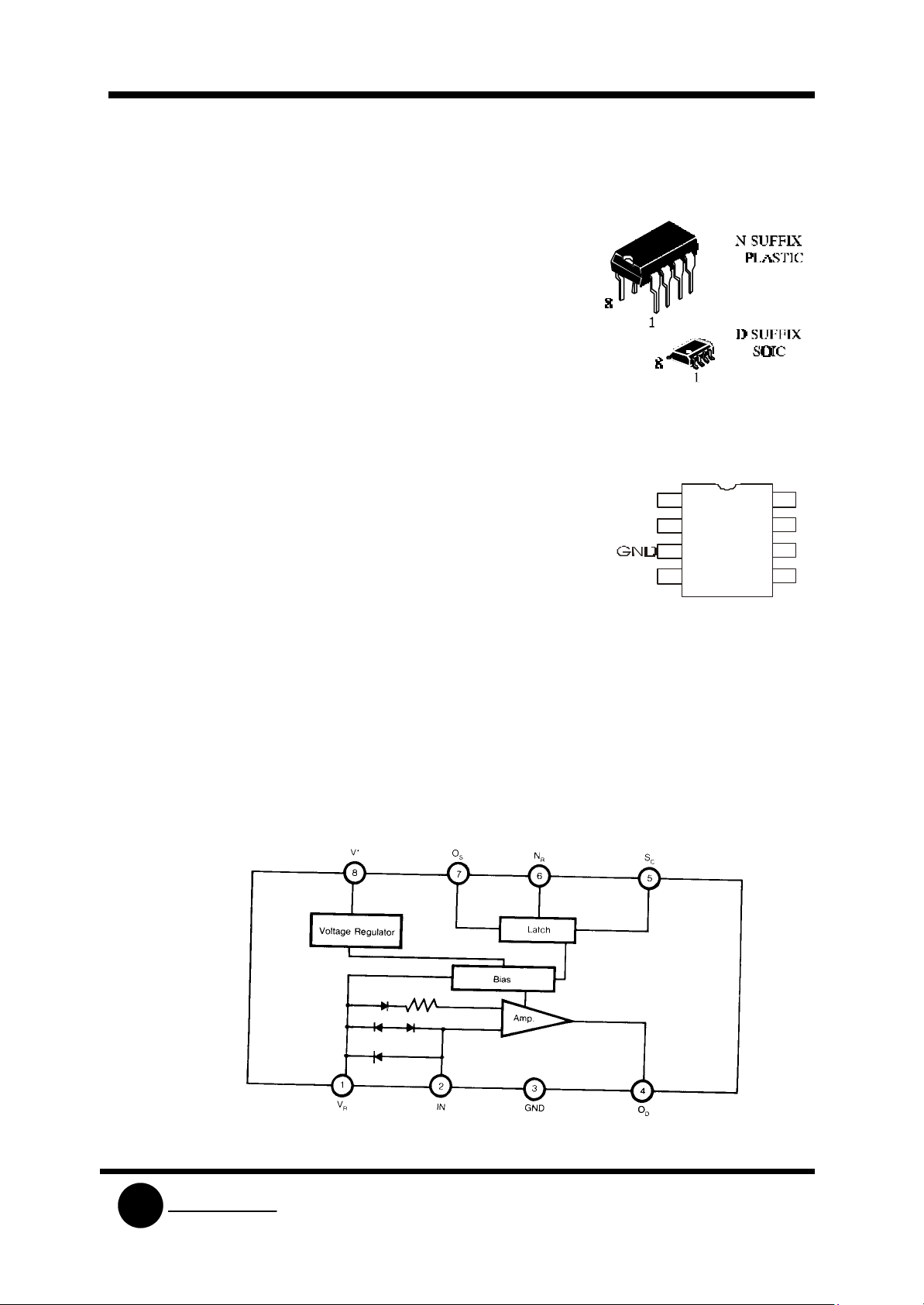
The SL7101 is designed for use in earth leakage circuit
interrupters for operation directly of the AC Line in breakers.
It contains pre regulator, main regulator, after regulator,
differential amplifier, leve l comparator, latch circuit. The input in
the differential amplifier is connect to the secondary node of
zero current transformer. The level comparator generates high
level when earth leakage current is greater than some level.
Feature
• Low Power Consumption (PD=5mW) 100V/200V
• 100V/200V Common Built-in Voltage Regulator
• High Gain Differential Amplifier
• High Input Sensitivity
• Minimum External Parts
• Large Surge Margin
• Wide Operating Temperature Range (TÀ=-30 to 85°C)
• High Noise Immunity
Pin Configuration
V
R
IN
O
D
(Top View )
1
2
3
4
8
7
6
5
+
V
O
N
R
S
C
Absolute Maximum Ratings (T^=25°c)
§ Supply Voltage
§ Supply Current
§ Power Dissipation
§ Operating Temperature
§ Storage Temperature
- 30 to 85°C
- 55 to 125°C
20V
8mA
200mW
Block Diagram
System Logic
SLS
Semiconductor
Page 2
SL7101
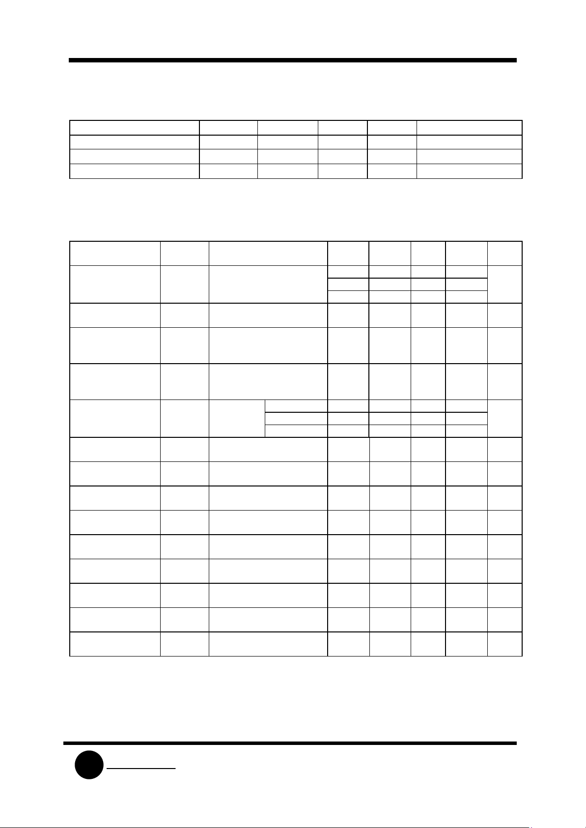
Recomended Operating Condition: TA=-30°C to 80°C
PARAMETER SYMBOL MIN. TYP. MAX UNIT
Supply Voltage V+ 12 V
Vs-GND Capacitor Cvs 1 µF
OS-GND Capacitor Cos 1 µF
Electrical Characteristics
PARAMETER
Supply Current 1 lS1
* Trip Voltage VT V+ = 16V,
Differential
Amplifier
Output Current 1
Differential
Amplifier Output
current 2
Output Current IO
S
ON Voltage V
C
SC Input Current ISC ON V+ = l2V
Output "L" Current I
Input Clamp
Voltage
Differential Input
Clamp Voltaqe
Max. Current
Voltage
Supply Current 2 IS2 VOS = 0.5 V,
Latch Circuit Off
Supply Votaqe
Response Time TON V+ = 16 V,
* A: 9 ~12.5 B: 11.5~15.5 C: 14.5~18
SYMBOL
CONDTIONS TEMP.
MIN. TYP. MAX. UNIT
(°C)
V+=12V,
VR - VI = 30 mV
VR - VI = X
I
V+ = 16 V,
TD1
-30 - - 580
25 300 400 530
µA
85 - - 480
-30
85
9 13.5 18 mV
(rms)
25 -12 -20 -30 µA
VR - VI = 30 mV
VOD = 1.2 V
I
V+ = 16 V,
TD2
V
- V
R
= short
I
25 17 27 37 µA
VOD = 0.8 V
VSC = 1.4 V
VOS = 0.8 V
lSI = 580µA -30 -200 -
lSI = 530µA 25 -100 -
µA
lSI = 480µA 85 -75 -
ON V+ = 16 V
SC
25 0.7 1.0 1.4 V
25 - - 5 µA
V+ = 12 V,
OSL
V
= 0.2 V
OSL
VIC V+ = 12 V,
IIC = 20 mA
V
IDC
I
= 100mA
IDC
VSM ISM = 7 mA
-30
200 800 1400 µA
85
-30
4.3 - 6.7 V
85
-30
0.4 1.2 2 V
85
25 20 24 28 V
V
- VI = X
R
-30
85
- - 1200 µA
V+ OFF 25 0.5 V
25 1 3 4 ms
V
- VI = 0.3 V
R
System Logic
SLS
Semiconductor
Page 3
SL7101
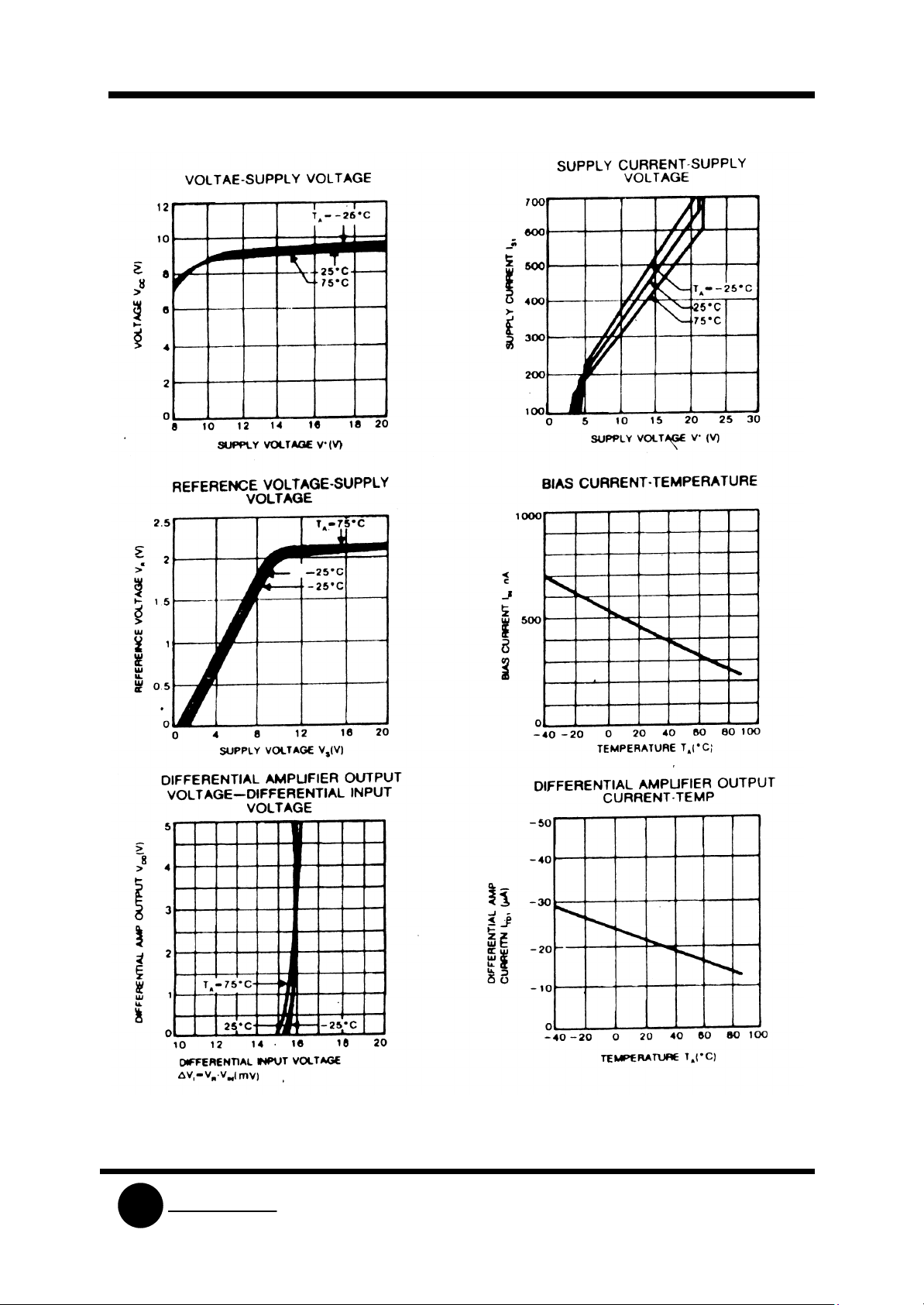
Typical Performance Curves
System Logic
SLS
Semiconductor
Page 4
SL7101
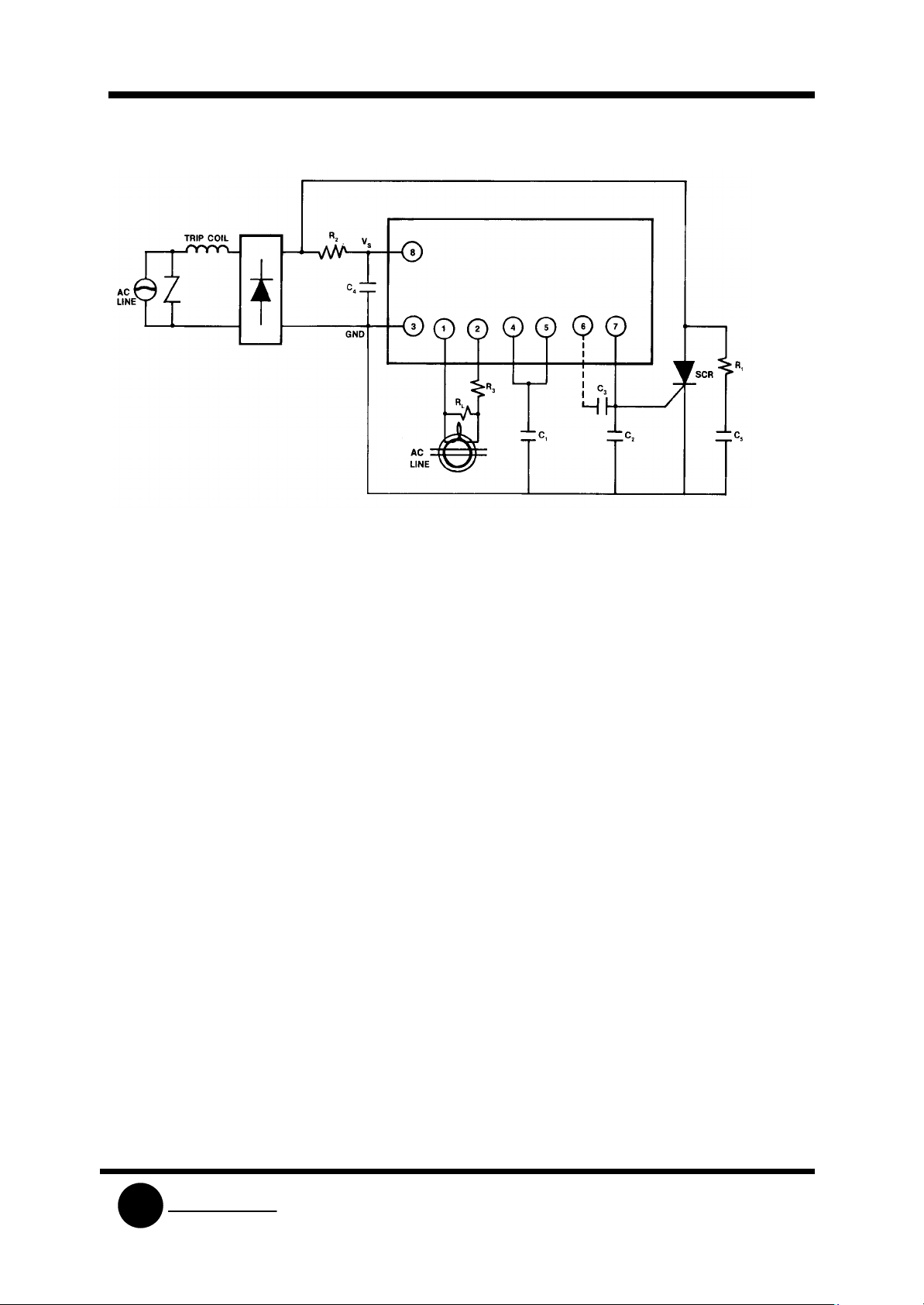
Typical Application
Description of elements of application diagram
1. The resistance of R1 resistor is chosen in such a way so that to limit IC’s consumption
current (not more than 8 mA), and here the voltage drop is around 21-28V.
2. R2 resistor provides the necessary bias of the differential cascade.
3. R3 resistor is a loading one per input.
4. R4 resistor limits the charging current of C4 electrolytic capacitor are required to maintain
IC performance until the fuse is completely burn out. Its value is chosen correspondingly.
5. C1 electrolytic capacitor is a filtering one as per supply (around 1 – 10 µF ).
6. Ñ2 and C3 capacitors are filtering ones (not more than 1 µF)
System Logic
SLS
Semiconductor
 Loading...