

Page 1
Features
● 400MHz Bandwidth (R
● High voltage Gain 45dB (R
● 70dB Gain Control Range
● High Output Level at Low Gain
● Surface Mount Plastic Package
● Low Cost
=50Ω)
L
=1kΩ)
L
Applications
● RF/IF Amplifier
● High Gain Mixers
● Video Amplifiers
Description
The SL6140 is an integrated broadband AGC amplifier,
designed on an advanced bipolar process. The
amplifier provides over 15dB of linear gain into 50Ω at
400MHz. Gain control is also provided with over 70dB
of dynamic range. The SL6140 offers over 45dB of
voltage gain with an RL of 1kΩ.
SL6140
SL6140
400MHz Wideband AGC Amplifier
DS2159 Issue no 5.0 July 1999
Ordering Information
SL6140/NA/MP Industrial temperature range
SL6140/NA/MPTC Tape and Reel
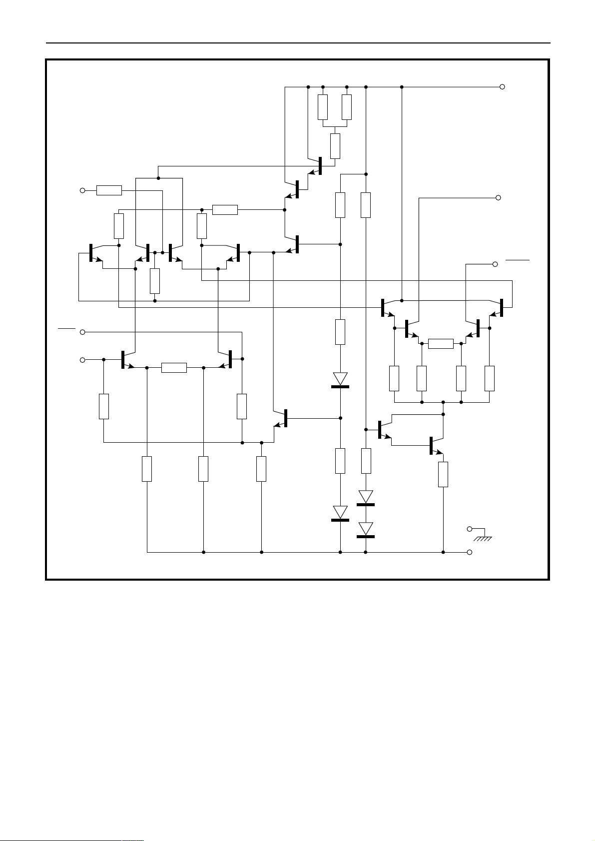
The SL6140 (Figure 3) is a high gain amplifier with an
AGC control capable of reducing the gain of the amplifier
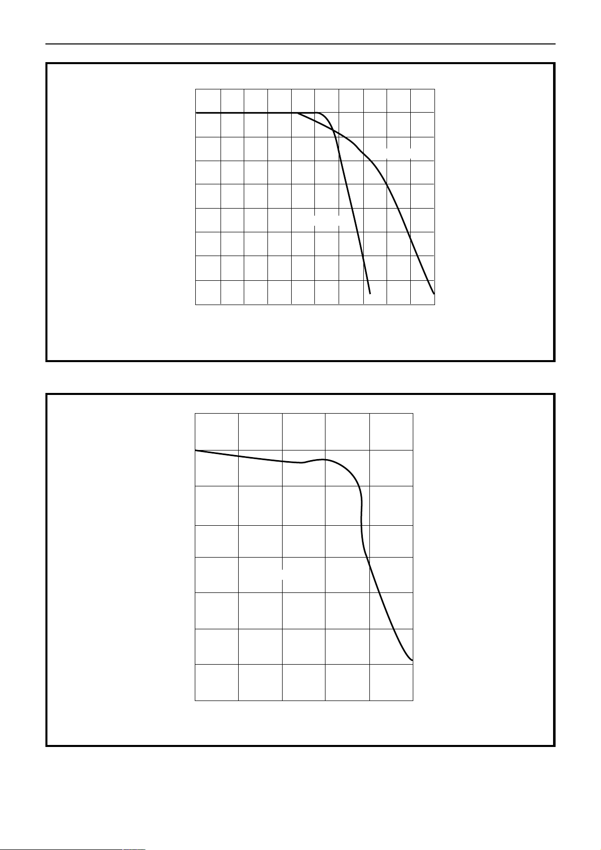
by over 70dB. The gain is adjustable by applying a
voltage to the AGC input via an external resistor (R
the value of which adjusts the curve of gain reduction
versus control voltage (see Figure 4). As the output
stage of the amplifier is an open collector the maximum
voltage gain is determined by RL. With load resistance
of 1kΩ the single ended voltage gain is 45dB and with a
load resistance of 50Ω the voltage gain is 15dB (20log
V
OUT/VIN
). Another parameter that depends on the load
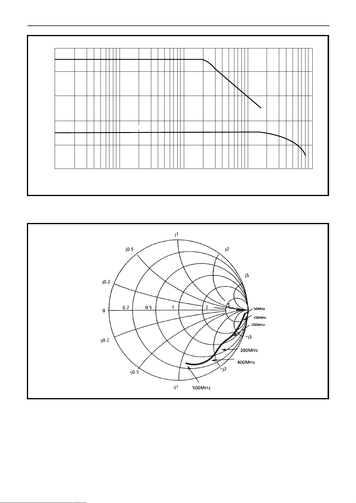
resistance is the bandwidth: 25MHz for RL = 1kΩ, as
compared with 400MHz for RL = 50Ω. RL is chosen to
give either the required bandwidth or voltage gain for the
circuit.
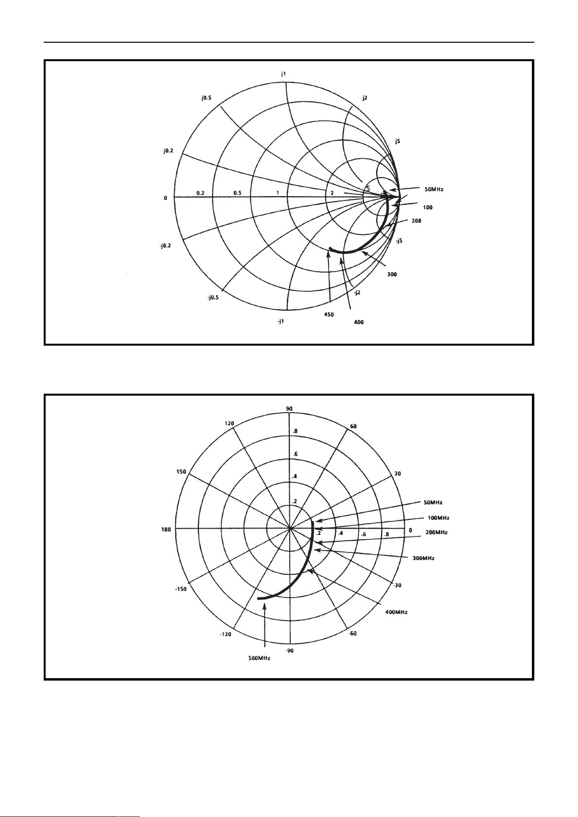
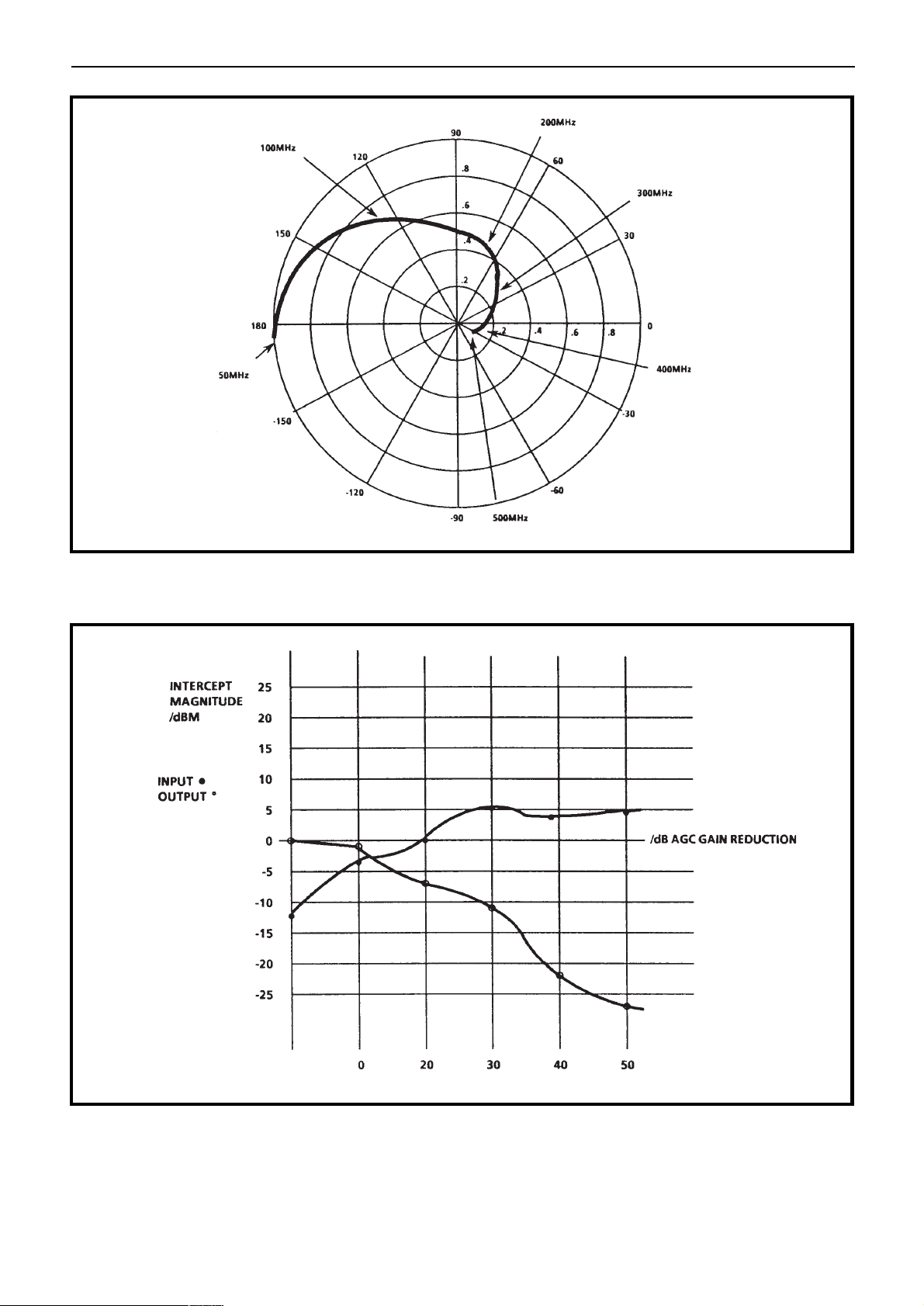
Figure 7 through to 10 show the typical S parameters for
the device. Figures 11 and 12 show the typical variation
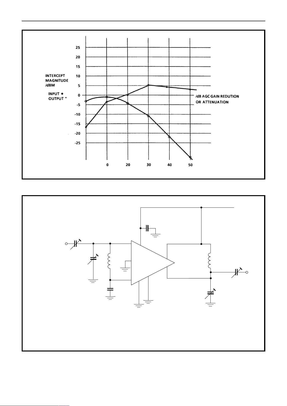
in 3rd order intercept performance with AGC.
In any application, the substrate should be connected to
the most negative point in the circuit, usually to the same
point as pin 3.
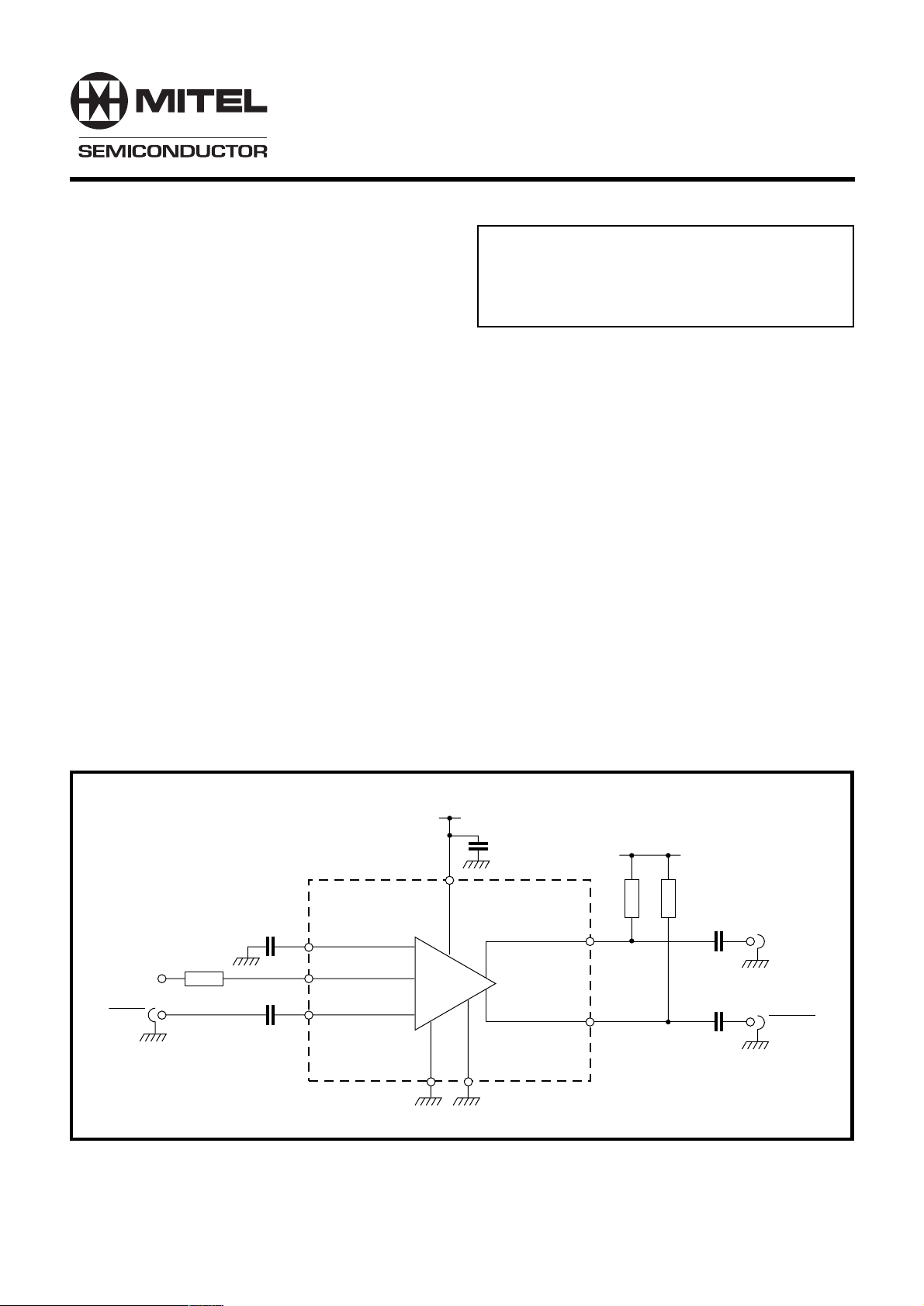
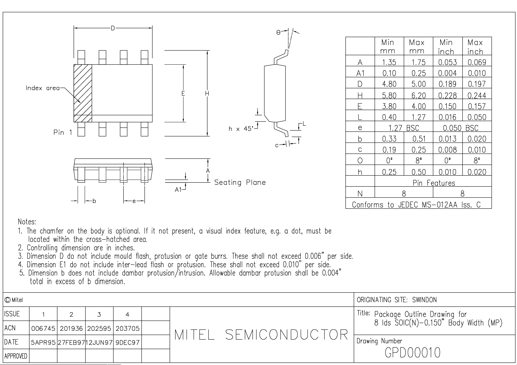
miniature plastic package
AGC
10
),
AGC
INPUT
INPUT
R
AGC
10n
10n
+VCC
1.0 F
2
6
5
SL6140
4
37
Figure 1 Typical Application
8
1
RLR
+VCC
L
10n
OUTPUT
10n
OUTPUT
1
Page 2
SL6140
OUTPUT
+V
CC
GROUND INPUT
INPUT
18
27
36
45
OUTPUT
GROUND
AGC INPUT
MP8
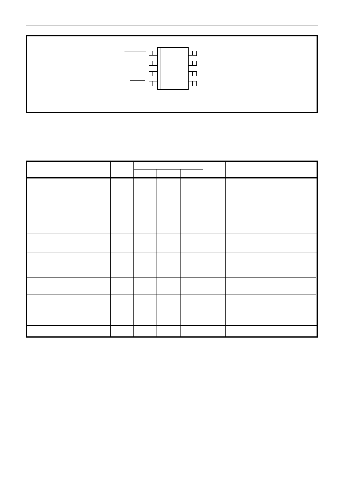
Figure 2 Pin Connections Diagram (top view)
Electrical Characteristics
T
= 25°C, VCC = 12V +5%, VIN = 1mV
amb
These characteristics are guaranteed over the following conditions (unless otherwise stated)
Characteristic
Supply current
Output stage current
Output current matching
(magnitude of difference of output
currents)
Pin
5,6,7
5,6
(sum)
5,6
, Frequency = 6MHz, Load (RL) = 10KOHms, R
RMS
Value
TypMin
19
5
7
1.0
Max
23
9
Units
mA
mA
mA
No input signal
No input signal
Conditions
= 22KOHm
AGC
AGC range
Voltage gain (single ended)
Bandwidth (-3dB)
Maximum output level (single
ended)
0dB AGC
-30dB AGC
Noise figure
Note. 1 Guaranteed but not tested.
2
5,6
5,6
5,6
5,6
5,6
5,6
60
40
Absolute Maximum Ratings
Supply voltage, V
Input voltage (differential) +5V
AGC supply V
Storage temperature -55°C to +150°C
Operating temperature range
SL6140 MP -40°C to +85°C
Chip operating temperature
SL6140 MP +150°C
CC
at 200mW
+18V
CC
75
45
55
15
25
400
3.5
3.5
5
Thermal Resistance
Chip-to-ambient
SL6140 MP 163°C/W
Chip-to-case
SL6140 MP 57°C/W
dB
dB
dB
dB
MHz
V p-p
V p-p
dB
See Figure 4 & Note 1
(VAGC = 0V to 10V)
R
= 1kΩ See Figure 5 & Note 1
L
Tuned input and output
R
= 50Ω
L
RL = 1kΩ See Figure 5
RL = 50Ω
Note 1
R
= 1kΩ. Note 1
L
Test CCT Figure 13
2
Page 3
180
470
X 2
SL6140
2
V
CC
AGC
INPUT
INPUT
70
5
I/P
2k
4
6
66
180
470470
5k5k
2.1k1.1k1.1k
7k 12.1k
1.4k
5.6k
1.9k
45
2.8k 2.8k200 200
200
1
8
OUTPUT
OUTPUT
Figure 3 Full Circuit Diagram of SL6140
7
3
SUBSTRATE
GROUND
3
Page 4
SL6140
G
A
I
N
R
E
D
U
C
T
I
O
N
(dB)
0
10
20
30
40
R
=5.6k
50
60
70
1 2 3 4 5 6 7 8 9100
AGC
AGC VOLTAGE
Figure 4 Gain Reduction v. AGC Voltage
R
AGC
=22k
D
I
F
F
E
R
E
N
T
I
A
L
O
U
T
P
U
T
(V p-p)
8
7
6
5
4
1MHzSINEWAVE
3
2
1
0
10 20 30 40 500
GAIN REDUCTION (dB)
Figure 5 Max Differential O/P Voltage v. Gain Reduction
4
Page 5
dB
G
A
N
SL6140
50
RL=1kΩ
40
30
I
20
10
RL=50Ω
0
0.1 10 100 1000
FREQUENCY (MHz)
Figure 6 Voltage Gain v. Frequency
Figure 7 Input Impedance 50Ω System
5
Page 6
SL6140
Figure 8 Output Impedance 50Ω System
Figure 9 Reverse Transmission Coefficient S12 SL6140
6
Page 7
SL6140
Figure 10 Forward Transmission Coefficient S12 SL6140
Figure 11 3rd Order Intercept Point Against Gain Reduction At 250.0MHz and 254.0MHz
7
Page 8
SL6140
Figure 12 3rd Order Intercept Point Against Gain Reduction At 100.0MHz and 104.0MHz
+12V
1nF
6
2
1nF
L1
5
4
7
3
1
8
L2
O/P
VARIABLE CAPS 3-25pF
L1 7 TURNS # 18 SWG 8mm DIA 16mm LONG
L2 6 TURNS # 16 SWG 14mm DIA 19mm LONG
Figure 13 50MHz Noise Figure Test Circuit
8
Page 9
Page 10

http://www.mitelsemi.com
World Headquarters - Canada
Tel: +1 (613) 592 2122
Fax: +1 (613) 592 6909
North America Asia/Pacific Europe, Middle East,
Tel: +1 (770) 486 0194 Tel: +65 333 6193 and Africa (EMEA)
Fax: +1 (770) 631 8213 Fax: +65 333 6192 Tel: +44 (0) 1793 518528
Fax: +44 (0) 1793 518581
Information relating to products and services furnished herein by Mitel Corporation or its subsidiaries (collectively “Mitel”) is believed to be reliable. However, Mitel assumes no
liability for errors that may appear in this publication, or for liability otherwise arising from the application or use of any such information, product or service or for any infringement of
patents or other intellectual property rights owned by third parties which may result from such application or use. Neither the supply of such information or purchase of product or
service conveys any license, either express or implied, under patents or other intellectual property rights owned by Mitel or licensed from third parties by Mitel, whatsoever.
Purchasers of products are also hereby notified that the use of product in certain ways or in combination with Mitel, or non-Mitel furnished goods or services may infringe patents or
other intellectual property rights owned by Mitel.
This publication is issued to provide information only and (unless agreed by Mitel in writing) may not be used, applied or reproduced for any purpose nor form part of any order or
contract nor to be regarded as a representation relating to the products or services concerned. The products, their specifications, services and other information appearing in this
publication are subject to change by Mitel without notice. No warranty or guarantee express or implied is made regarding the capability, performance or suitability of any product or
service. Information concerning possible methods of use is provided as a guide only and does not constitute any guarantee that such methods of use will be satisfactory in a specific
piece of equipment. It is the user’s responsibility to fully determine the performance and suitability of any equipment using such information and to ensure that any publication or
data used is up to date and has not been superseded. Manufacturing does not necessarily include testing of all functions or parameters. These products are not suitable for use in
any medical products whose failure to perform may result in significant injury or death to the user. All products and materials are sold and services provided subject to Mitel’s
conditions of sale which are available on request.
M Mitel (design) and ST-BUS are registered trademarks of MITEL Corporation
Mitel Semiconductor is an ISO 9001 Registered Company
Copyright 1999 MITEL Corporation
All Rights Reserved
Printed in CANADA
TECHNICAL DOCUMENTATION - NOT FOR RESALE
 Loading...