

Page 1
SL4093B
Semiconductor
Quad 2-Input NAND Schmitt Triggers
High-Voltage Silicon-Gate CMOS
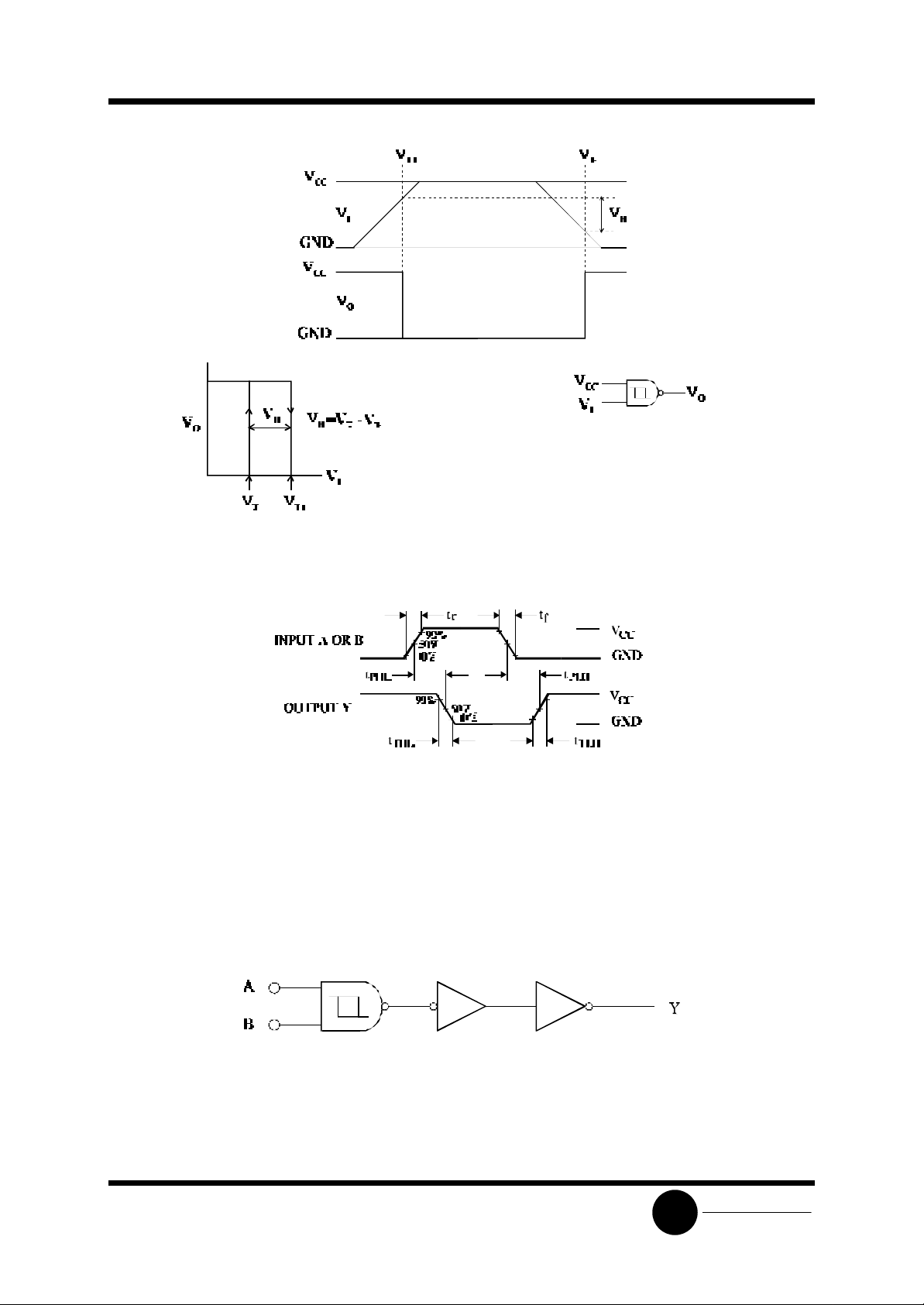
The SL4093B consists of four Schmitt-trigger circuits. Each circuit
functions as a two-input NAND gate with Schmitt-trigger action on
both inputs. The gate switches at different points for positive- and
negative- going signals. The difference between the positive voltage
(VP) and the negative voltage (VN) is defined as hysteresis voltage (VH)
(see Fig.1).
• Operating Voltage Range: 3.0 to 18 V
• Maximum input current of 1 µA at 18 V over full package-
temperature range; 100 nA at 18 V and 25°C
• Noise margin (over full package temperature range):
1.0 V min @ 5.0 V supply
2.0 V min @ 10.0 V supply
2.5 V min @ 15.0 V supply
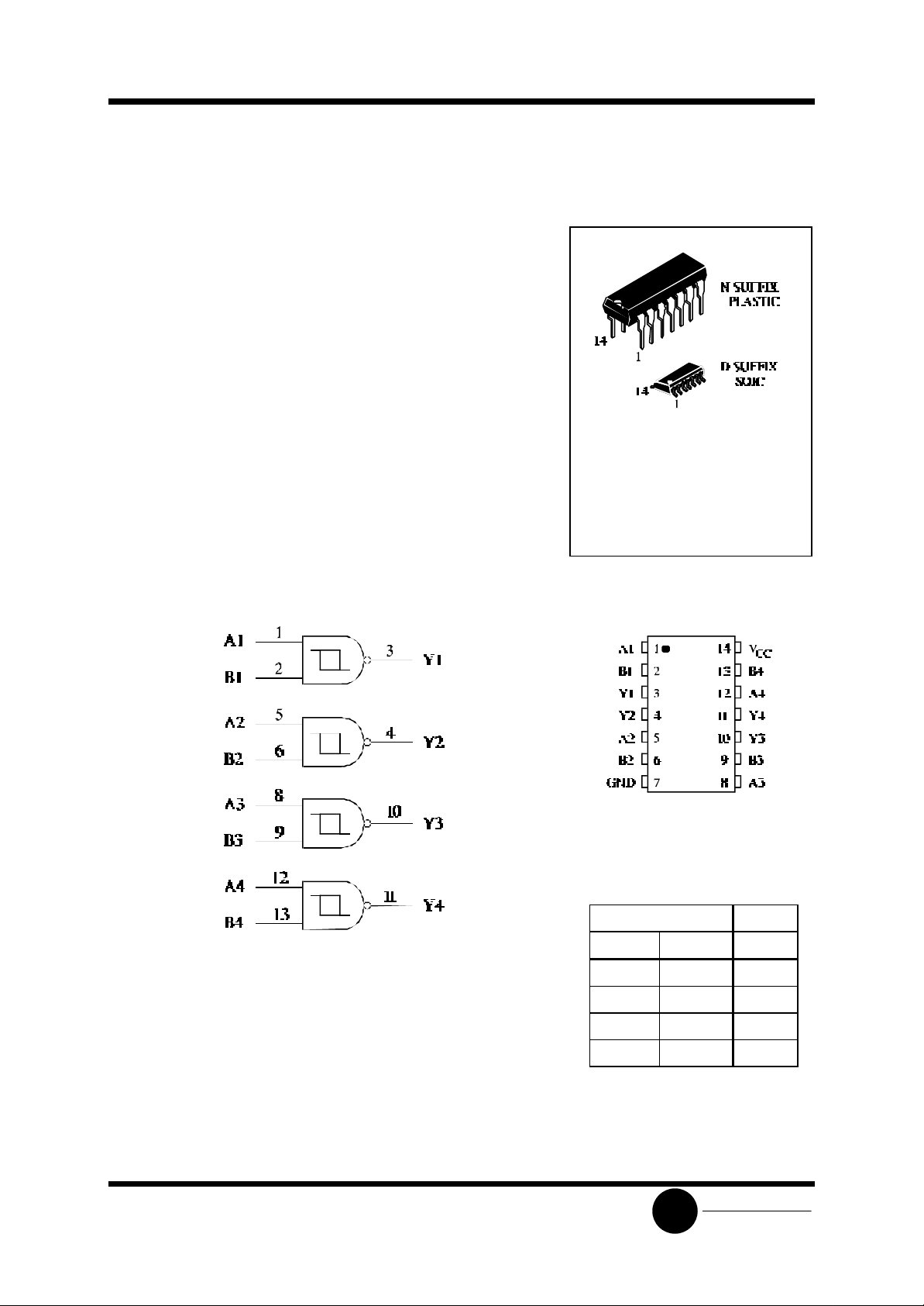
LOGIC DIAGRAM
ORDERING INFORMATION
SL4093BN Plastic
SL4093BD SOIC
TA = -55° to 125° C for all packages
PIN ASSIGNMENT
PIN 14 =VCC
PIN 7 = GND
FUNCTION TABLE
Inputs Output
A B Y
L L H
L H H
H L H
H H L
System Logic
SLS
Page 2
SL4093B
Semiconductor
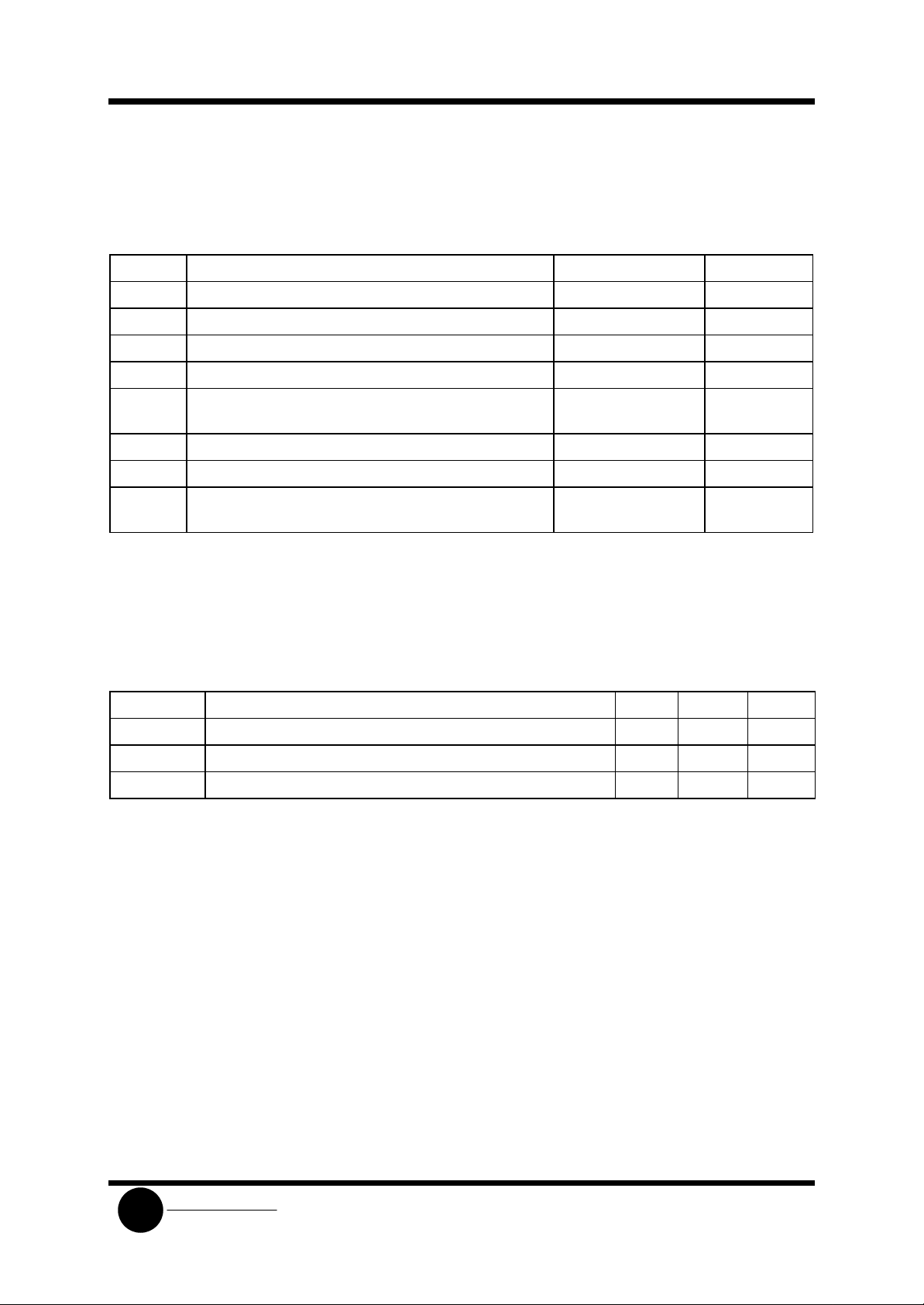
MAXIMUM RATINGS*
Symbol Parameter Value Unit
VCC DC Supply Voltage (Referenced to GND) -0.5 to +20 V
VIN DC Input Voltage (Referenced to GND) -0.5 to VCC +0.5 V
V
DC Output Voltage (Referenced to GND) -0.5 to VCC +0.5 V
OUT
IIN DC Input Current, per Pin ±10 mA
PD Power Dissipation in Still Air, Plastic DIP+
SOIC Package+
PD Power Dissipation per Output Transistor 100 mW
Tstg Storage Temperature -65 to +150 °C
TL Lead Temperature, 1 mm from Case for 10 Seconds
(Plastic DIP or SOIC Package)
*
Maximum Ratings are those values beyond which damage to the device may occur.
Functional operation should be restricted to the Recommended Operating Conditions.
+Derating - Plastic DIP: - 10 mW/°C from 65° to 125°C
SOIC Package: : - 7 mW/°C from 65° to 125°C
750
500
260 °C
RECOMMENDED OPERATING CONDITIONS
Symbol Parameter Min Max Unit
VCC DC Supply Voltage (Referenced to GND) 3.0 18 V
VIN, V
DC Input Voltage, Output Voltage (Referenced to GND) 0 VCC V
OUT
TA Operating Temperature, All Package Types -55 +125 °C
mW
This device contains protection circuitry to guard against damage due to high static voltages or electric
fields. However, precautions must be taken to avoid applications of any voltage higher than maximum rated
voltages to this high-impedance circuit. For proper operation, VIN and V
GND≤(VIN or V
Unused inputs must always be tied to an appropriate logic voltage level (e.g., either GND or VCC).
Unused outputs must be left open.
System Logic
SLS
OUT
)≤VCC.
should be constrained to the ra nge
OUT
Page 3
SL4093B
Semiconductor
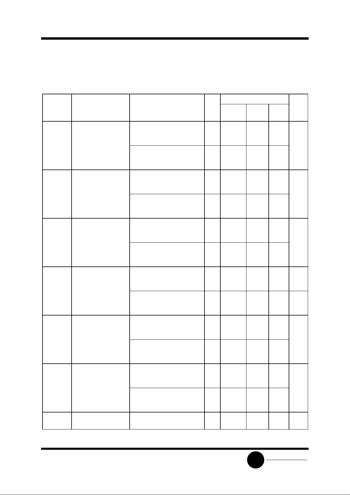
DC ELECTRICAL CHARACTERISTICS(Voltages Referenced to GND)
VCC Guaranteed Limit
Symbol Parameter Test Conditions V ≥-55°C 25°C ≤125
°C
VT+min Minimum Positive-
Going Input
Threshold Voltage
Input on terminals A and B;
VT+max Maximum Positive-
Going Input
Threshold Voltage
Input on terminals A and B;
VT-min Minimum Negative-
Going Input
Threshold Voltage
Input on terminals A and B;
VT-max Maximum Negative-
Going Input
Threshold Voltage
Input on terminals A or B;
other inputs to VCC
other inputs to VCC
Input on terminals A or B;
other inputs to VCC
other inputs to VCC
Input on terminals A or B;
other inputs to VCC
other inputs to VCC
Input on terminals A or B;
other inputs to VCC
5.0
10
15
5.0
10
15
5.0
10
15
5.0
10
15
5.0
10
15
5.0
10
15
5.0
10
15
2.2
4.6
6.8
2.6
5.6
6.3
3.6
7.1
10.8
4
8.2
12.7
0.9
2.5
4
1.4
3.4
4.8
2.8
5.2
7.4
2.2
4.6
6.8
2.6
5.6
6.3
3.6
7.1
10.8
4
8.2
12.7
0.9
2.5
4
1.4
3.4
4.8
2.8
5.2
7.4
2.2
4.6
6.8
2.6
5.6
6.3
3.6
7.1
10.8
4
8.2
12.7
0.9
2.5
4
1.4
3.4
4.8
2.8
5.2
7.4
Unit
V
V
V
V
Input on terminals A and B;
other inputs to VCC
VHmin
Note
VHmax
Note
IIN Maximum Input
Minimum Hysteresis
Voltage
Input on terminals A and B;
Maximum Hysteresis
Voltage
Input on terminals A and B;
Leakage Current
Input on terminals A or B;
other inputs to VCC
other inputs to VCC
Input on terminals A or B;
other inputs to VCC
other inputs to VCC
VIN= GND or VCC 18 ±0.1 ±0.1 ±1.0 µA
5.0
10
15
5.0
10
15
5.0
10
15
5.0
10
15
5.0
10
15
3.2
6.6
9.6
0.3
1.2
1.6
0.3
1.2
1.6
1.6
3.4
5
1.6
3.4
5
3.2
6.6
9.6
0.3
1.2
1.6
0.3
1.2
1.6
1.6
3.4
5
1.6
3.4
5
SLS
3.2
6.6
9.6
0.3
1.2
1.6
0.3
1.2
1.6
1.6
3.4
5
1.6
3.4
5
System Logic
V
V
Page 4
Semiconductor
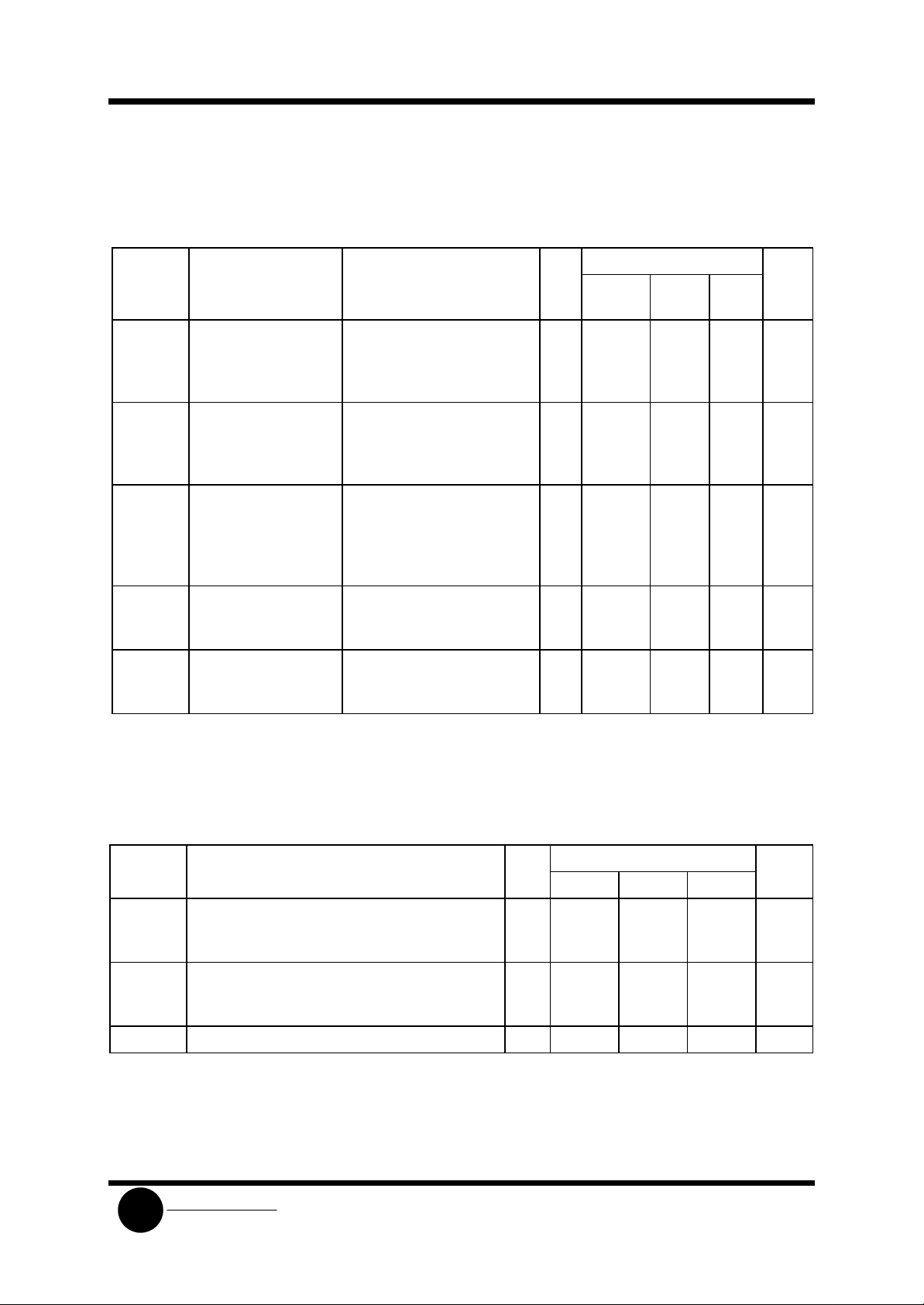
DC ELECTRICAL CHARACTERISTICS(Voltages Referenced to GND) - continued
VCC Guaranteed Limit
SL4093B
Symbol Parameter Test Conditions V ≥-55°C 25°C ≤125
ICC Maximum Quiescent
Supply Current
(per Package)
IOL Minimum Output Low
(Sink) Current
IOH Minimum Output High
(Source) Current
VOH Minimum High-Level
Output Voltage
VOL Maximum Low -Level
Output Voltage
Note. VHmin>(VT+min) -(VT-max); VHmax=(VT+max)+(VT-min).
VIN= GND or VCC 5.0
10
15
20
VIN= GND or VCC
UOL=0.4 V
UOL=0.5 V
UOL=1.5 V
VIN= GND or VCC
UOH=2.5 V
UOH=4.6 V
UOH=9.5 V
UOH=13.5 V
VIN=GND or VCC 5.0
VIN= VCC 5.0
5.0
10
15
5.0
5.0
10
15
10
15
10
15
1
2
4
20
0.64
1.6
4.2
-2.0
-0.64
-1.6
-4.2
4.95
9.95
14.95
0.05
0.05
0.05
1
2
4
20
0.51
1.3
3.4
-1.6
-0.51
-1.3
-3.4
4.95
9.95
14.95
0.05
0.05
0.05
°C
30
60
120
600
0.36
0.9
2.4
-1.15
-0.36
-0.9
-2.4
4.95
9.95
14.95
0.05
0.05
0.05
Unit
µA
mA
mA
V
V
AC ELECTRICAL CHARACTERISTICS(C
VCC Guaranteed Limit
Symbol Parameter V ≥-55°C 25°C ≤125°C Unit
t
, t
Maximum Propagation Delay, Input A or B to
PHL
Output Y (Figure 2)
, t
Maximum Output Transition Time, Any Output
THL
(Figure 2)
CIN Maximum Input Capacitance - 7.5 pF
System Logic
PLH
t
TLH
SLS
=50pF, RL=200kΩ, Input tr=tf=20 ns)
L
5.0
10
15
5.0
10
15
380
180
130
200
100
80
380
180
130
200
100
80
760
360
260
400
200
160
ns
ns
Page 5
SL4093B
Semiconductor
a) Definition of VT+, VT-, V
b) Transfer characteristic of 1 of 4 gates
Figure 1. Hysteresis definition, characteristic, and test setup
Figure 2. Switching Waveforms
EXPANDED LOGIC DIAGRAM
(1/4 of the Device)
H
c) Test setup
System Logic
SLS
 Loading...