

Page 1
SL4066B
Semiconductor
Quad Bilateral Switch
High-Voltage Silicon-Gate CMOS
The SL4066B is a quad bilateral switch intended for the
transmission or multiplexing of analog or digital signals. In addition, the
on-state resistance is relatively constant over the full input-signal
range.
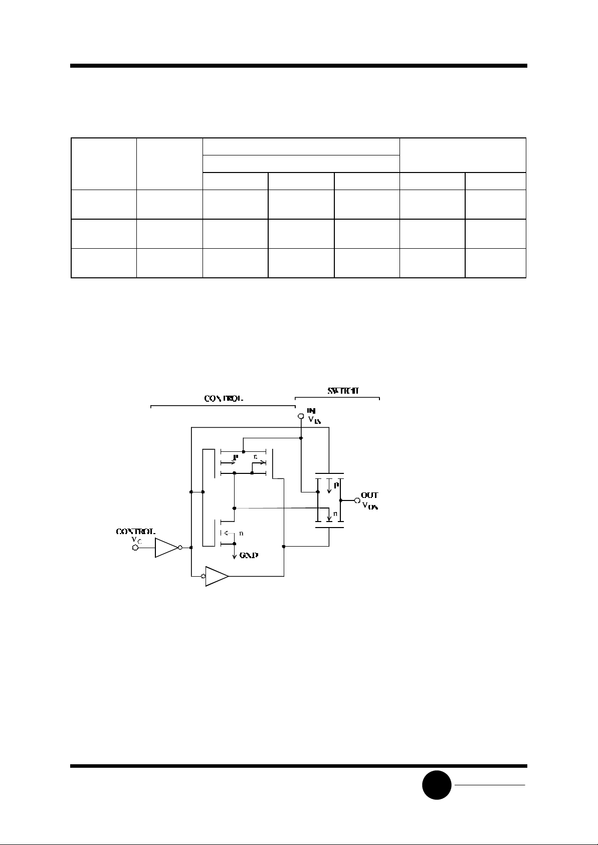
The SL4066B consists of four independent bilateral switches. A
single control signal is required per switch. Both the p and the n device
in a given switch are biased on or off simultaneously by the control
signal.(As show in Fig.1.)The well of the n-channel device on each
switch is either tied to the input when the switch is on or to GND when
the switch is off. This configuration eliminates the variation of the
switch-transistor threshold voltage with input signal, and thus keeps
the on-state resistance low over the full operating-signal range.
The advantages over single -channel switches include peak inputsignal voltage swings equal to the full supply voltage, and more
constant on-state impedance over the input-signal range.
• Operating Voltage Range: 3.0 to 18 V
• Maximum input current of 1 µA at 18 V over full package-
temperature range; 100 nA at 18 V and 25°C
• Noise margin (over full package temperature range) :
1.0 V min @ 5.0 V supply
2.0 V min @ 10.0 V supply
2.5 V min @ 15.0 V supply
ORDERING INFORMATION
SL4066BN Plastic
SL4066BD SOIC
TA = -55° to 125° C for all packages
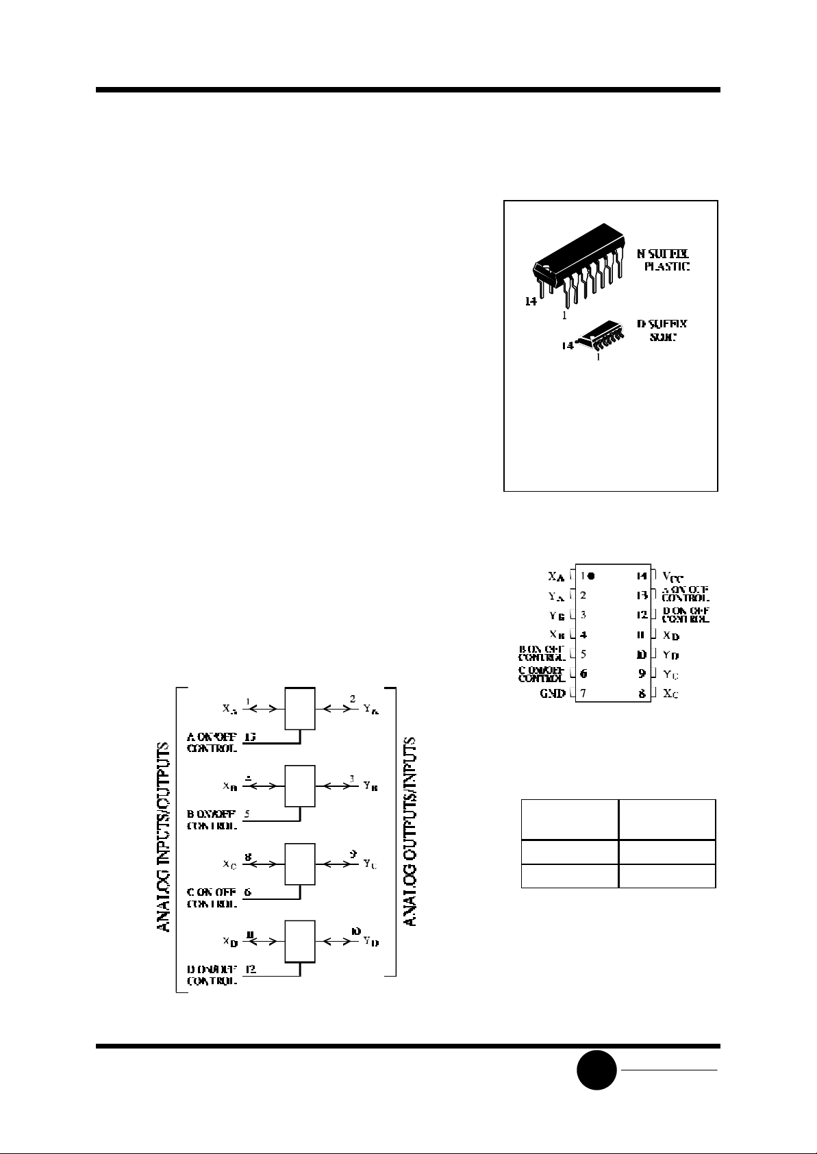
PIN ASSIGNMENT
LOGIC DIAGRAM
PIN 14 =VCC
PIN 7 = GND
FUNCTION TABLE
On/Off Control
Input
L Off
H On
State of
Analog Switch
SLS
System Logic
Page 2
SL4066B
Semiconductor
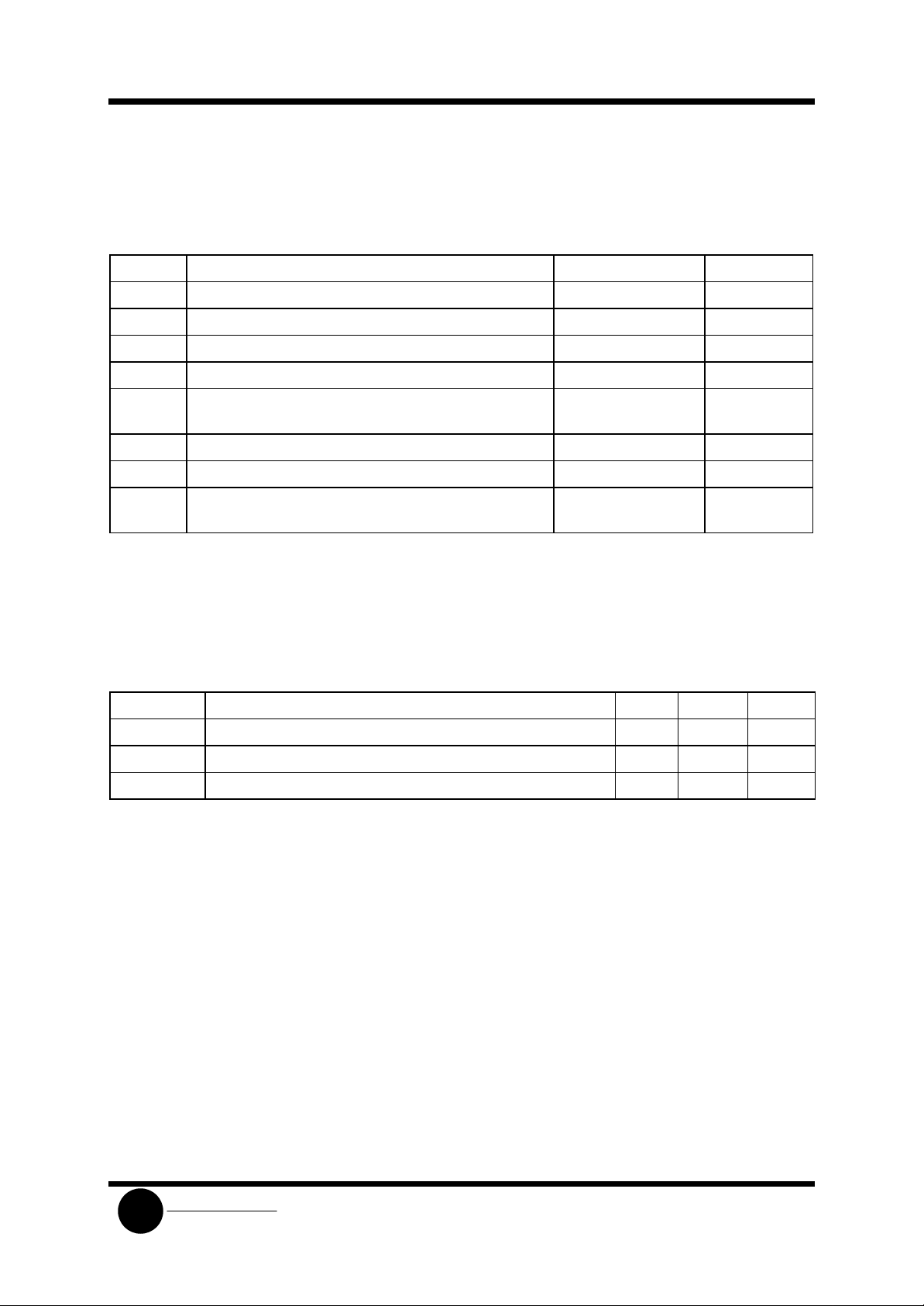
MAXIMUM RATINGS*
Symbol Parameter Value Unit
VCC DC Supply Voltage (Referenced to GND) -0.5 to +20 V
VIN DC Input Voltage (Referenced to GND) -0.5 to VCC +0.5 V
V
DC Output Voltage (Referenced to GND) -0.5 to VCC +0.5 V
OUT
IIN DC Input Current, per Pin ±10 mA
PD Power Dissipation in Still Air, Plastic DIP+
SOIC Package+
PD Power Dissipation per Output Transistor 100 mW
Tstg Storage Temperature -65 to +150 °C
TL Lead Temperature, 1 mm from Case for 10 Seconds
(Plastic DIP or SOIC Package)
*
Maximum Ratings are those values beyond which damage to the device may occur.
Functional operation should be restricted to the Recommended Operating Conditions.
+Derating - Plastic DIP: - 10 mW/°C from 65° to 125°C
SOIC Package: : - 7 mW/°C from 65° to 125°C
750
500
260 °C
RECOMMENDED OPERATING CONDITIONS
Symbol Parameter Min Max Unit
VCC DC Supply Voltage (Referenced to GND) 3.0 18 V
VIN, V
DC Input Voltage, Output Voltage (Referenced to GND) 0 VCC V
OUT
TA Operating Temperature, All Package Types -55 +125 °C
mW
This device contains protection circuitry to guard against damage due to high static voltages or electric
fields. However, precautions must be taken to avoid applications of any voltage higher than maximum rated
voltages to this high-impedance circuit. For proper operation, VIN and V
GND≤(VIN or V
Unused inputs must always be tied to an appropriate logic voltage level (e.g., either GND or VCC).
Unused outputs must be left open.
System Logic
SLS
OUT
)≤VCC.
should be constrained to the range
OUT
Page 3
SL4066B
Semiconductor
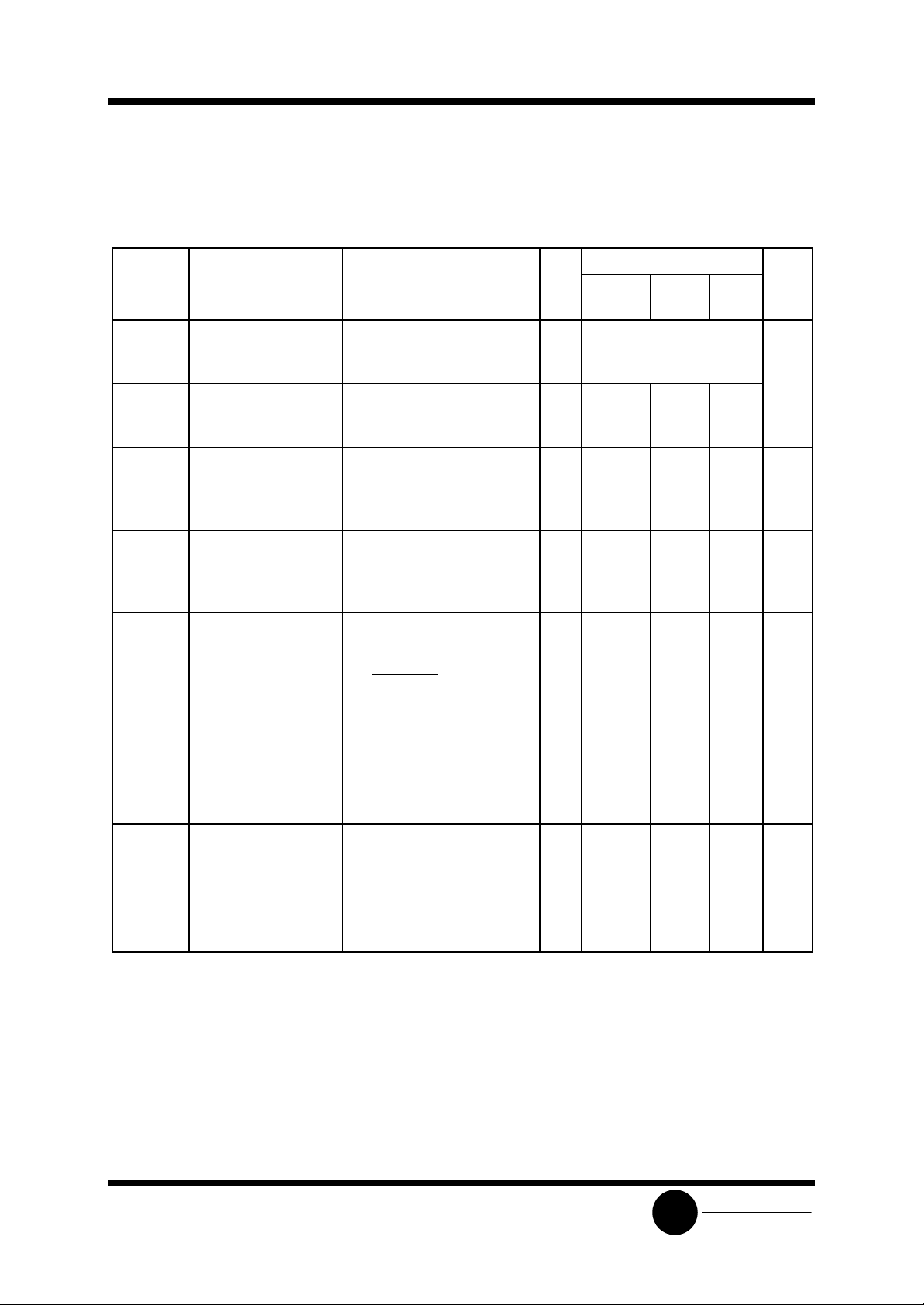
DC ELECTRICAL CHARACTERISTICS(Voltages Referenced to GND)
VCC Guaranteed Limit
Symbol Parameter Test Conditions V ≥-55°C 25
°C
VIH Minimum High-Level
Voltage ON/Off
Control Inputs
VIL Minimum Low -Level
Voltage ON/Off
Control Inputs
IIN Maximum Input
Leakage Current,
ON/OFF Control
Inputs
ICC Maximum Quiescent
Supply Current
(per Package)
RON Maximum “ON”
Resistance
∆RON Maximum Difference
in “ON” Resistance
Between Any Two
Channels in the Same
Package
RON= Per Spec 5.0
10
15
R
= Per Spec 5.0
ON
10
15
VIN = VCC or GND 18 ±0.1 ±0.1 ±1.0 µA
VIN = VCC or GND 5.0
10
15
20
VC= VCC
RL=10 kΩ returned
V
- GND
CC
to
2
VIS= GND to VCC
VC= VCC
RL=10 kΩ
5.0
10
15
5.0
10
15
1
2
2
0.25
0.5
1
5
800
310
200
-
-
-
3.5(Min)
7(Min)
11(Min)
1
2
2
0.25
0.5
1
5
1050
400
240
15
10
5
≤125
°C
1
2
2
7.5
15
30
150
1300
550
320
-
-
-
Unit
V
V
µA
Ω
Ω
I
Maximum Off-Channel
OFF
Leakage Current, Any
One Channel
ION Maximum On-Channel
Leakage Current, Any
One Channel
VC= 0 V
VIS=18 V; VOS= 0 V
VIS=0 V; VOS= 18V
VC= 0 V
VIS=18 V; VOS= 0 V
VIS=0 V; VOS= 18V
18 ±0.1 ±0.1 ±1.0 µA
18 ±0.1 ±0.1 ±1.0 µA
System Logic
SLS
Page 4
SL4066B
Semiconductor
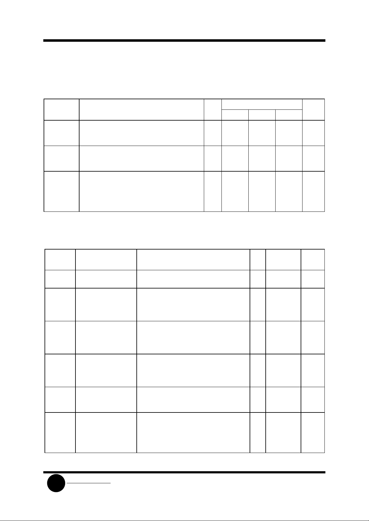
AC ELECTRICAL CHARACTERISTICS(C
=50pF, RL=200kΩ, Input tr=tf=20 ns)
L
VCC Guaranteed Limit
Symbol Parameter V ≥-55°C 25°C ≤125°C Unit
t
, t
PLH
Maximum Propagation Delay, Analog Input to
PHL
Analog Output (Figure 2)
t
, t
,
PLZ
t
PZL
PHZ
, t
Maximum Propagation Delay, ON/OFF Control
to Analog Output (Figure 3)
PZH
C Maximum Capacitance
ON/OFF Control Input
Control Input = GND
Analog I/O
Feedthrough
5.0
10
15
5.0
10
15
40
20
15
70
40
30
-
40
20
15
70
40
30
15
7.5
0.6
80
40
30
140
80
60
pF
ns
ns
ADDITIONAL APPLICATION CHARACTERISTICS(Voltages Referenced to GND Unless Noted)
VCC Limit*
Symbol Parameter Test Conditions V 25°C Unit
THD Total Harmonic
Distortion
BW Maximum On-Channel
Bandwidth or
V
= VCC , GND = -5 V
C
R
= 10 kΩ, f
L
V
= VCC , GND = -5 V
C
R
= 1 kΩ
L
IS
=1 kHz sine wave
Minimum Frequency
Response
BW Maximum On-Channel
Bandwidth or
V
= GND , VIS = 5 V
C
R
= 1 kΩ
L
Minimum Frequency
Response
BW Maximum On-Channel
Bandwidth or
Minimum Frequency
Response
- Cross talk (Control
Input to Signal
Output)
- Maximum Control
Input Repetition Rate
V
(A) = VCC = 5 V
C
V
(B) = GND = -5 V
C
V
(A) = 5 V
IS
R
= 1 kΩ
L
VC= 10 V
tr, tf = 20 ns
R
= 10 kΩ
L
VIS= VCC, R
C
L
L
= 50 pF
,50 Ω source
P - P
= 1 kΩ
VC= 10 V (square wave centered on 5 V)
tr, tf = 20 ns,
VOS= 1/2 V
*
Guaranteed limits not tested. Determined by design and verified by qualification.
@1 kHz
OS
5 0.4 %
5 40 MHz
10 1 MHz
5 8 MHz
10 50 mV
5
10
15
6
9
9.5
MHz
SLS
System Logic
Page 5
SL4066B
Semiconductor
Switch Input Switch Output,
IIS (mA) VOS (V)
VCC (V) VIS (V) -55 °C +25 °C +125 °C Min Max
5
5
10
10
15
15
0
5
0
10
0
15
0.64
-0.64
1.6
-1.6
4.2
-4.2
0.51
-0.51
1.3
-1.3
3.4
-3.4
0.36
-0.36
0.9
-0.9
2.4
-2.4
-
4.6
-
9.5
-
13.5
0.4
-
0.5
-
1.5
-
GND ≤ VIS ≤ VCC
Figure 1. Schematic diagram of 1 of 4 identical switches and its associated control circuitry.
System Logic
SLS
Page 6
SL4066B
Semiconductor
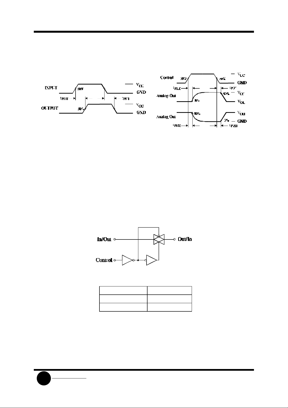
Figure 2. Switching Waveforms Figure 3. Switching Waveforms
EXPANDED LOGIC DIAGRAM
(1/4 of the Device)
SLS
Control Switch
GND = L OFF
VCC = H ON
System Logic
 Loading...