

Page 1
Low Voltage Audio Power AMP
SL386
The SL386 is a power amplifier designed for use in low voltage
consumer applications. The gain is internally set to 20 to keep external
part count low, but the addition of an external resistor and capacitor
between pins 1 and 8 will increase the gain to any value up to 200.
The inputs are ground referenced while the output is automatically
biased to one half the supply voltage. The quiescent powe r drain is
only 24 milliwatts when operating from a 6 volt supply, making the
SL386 ideal for battery operation.
• Battery Operation
• Minimum External Parts
• Wide Supply Voltage Range: 4 V - 12 V
• Low Quiescent Current Drain: 4 mA
• Voltage Gains from 20 to 200
• Ground Referenced Input
• Self-Centering Output Quiescent Voltage
• Low Distortion
• Eight Pin Dual -In-Line Package
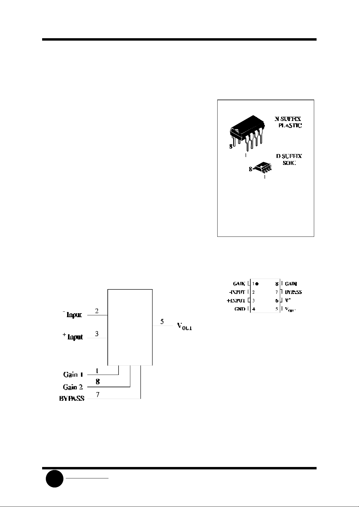
LOGIC DIAGRAM
ORDERING INFORMATION
SL386N Plastic
SL386D SOIC
TA = 0° to 70° C for
package
PIN ASSIGNMENT
Pin 4 = GND
Pin 6 = Supply Voltage V+
System Logic
SLS
Semiconductor
Page 2
SL386
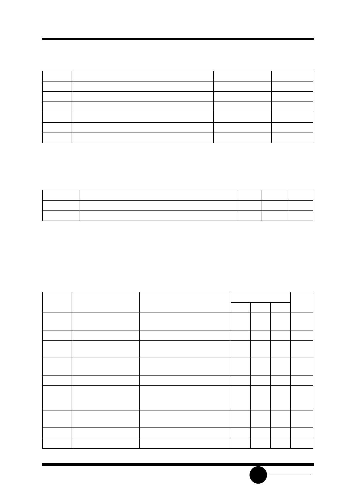
MAXIMUM RATINGS*
Symbol Parameter Value Unit
VCC Supply Voltage 15 V
VIN Input Voltage ±0.4 V
PD Power Dissipation 1.25 W
Tstg Storage Temperature -65 to +150 °C
TJ Junction Temperature +150 °C
TL Lead Temperature +300 °C
*
Maximum Ratings are those values beyond which damage to the device may occur.
Functional operation should be restricted to the Recommended Operating Conditions.
RECOMMENDED OPERATING CONDITIONS
Symbol Parameter Min Max Unit
VCC Supply Voltage 4.0 12 V
TA Operating Temperature, All Package Types 0 +70 °C
This device contains protection circuitry to guard against damage due to high static voltages or electric
fields. However, precautions must be taken to avoid applications of any voltage higher than maximum rated
voltages to this high-impedance circuit. For proper operation, VIN and V
GND≤(VIN or V
Unused inputs must always be tied to an appropriate logic voltage level (e.g., either GND or VCC).
Unused outputs must be left open.
OUT
)≤VCC.
should be constrained to the range
OUT
ELECTRICAL CHARACTERISTICS(T
Symbol Parameter Test Conditions Guara nteed Limits Unit
Min Typ Max
V+ Operating Supply
Voltage
I+ Quiescent Current V+ = 6 V, VIN = 0 8 mA
PO Output Power V+= 6V, RL =8Ω, THD=10%
AV Voltage Gain V+= 6V, f=1kHz
BW Bandwidth V+= 6V, Pins 1 and 8 Open 250 KHz
4 12 V
V+= 9V, RL =8Ω, THD=10%
10µF from Pin 1 and 8
= 25°C)
A
325
1000
26
46
mW
dB
THD Total Harmonic
Distortion
PSRR Power Supply Rejection
Ratio
RIN Input Resistance 30 80 KΩ
IB Input Bias Current V+= 6V, Pins 2 and 3 Open 250 nA
V+= 6V, RL =8Ω, P
f=1kHz,
Pins 1 and 8 Open
V+= 6V, f=1kHz, C
Pins 1 and 8 Open
=125mW,
OUT
BYPASS
=10µF,
3.0 %
45 dB
System Logic
SLS
Semiconductor
Page 3
APPLICATION INFORMATION
GAIN CONTROL
To make the SL386 a more versatile amplifier, two
pins (1 and 8) are provided for gain control. With
pins 1 and 8 open the 1.35 KΩ res istor sets the gain
at 20 (26 dB). If a capacitor is put from pin 1 to 8,
bypassing the 1.35 KΩ resistor, the gain will go up to
200 (46 dB). If a resistor is placed in series with the
capacitor, the gain can be set to any value from 20 to
200. Gain control can also be done by capacitively
coupling a resistor (or FET) from pin 1 to ground.
Additional external components can be placed in
parallel with the internal feedback resistors to tailor
the gain and frequency response for individual
applications. For example, we can compensate poor
speaker bass response by frequency shaping the
feeback path. This is done with a series RC from pin 1
to 5 (paralleling the internal 15 KΩ resistor). For 6 dB
effective bass boots: R≅15 KΩ, the lowest value for
good stable operation is R=10 KΩ if pin 8 is open. If
pins 1 and 8 are bypassed then R as low as 2 KΩ can
be used. This restriction is because the amplifier is
only compensated for closed-loop gains greater the
9.
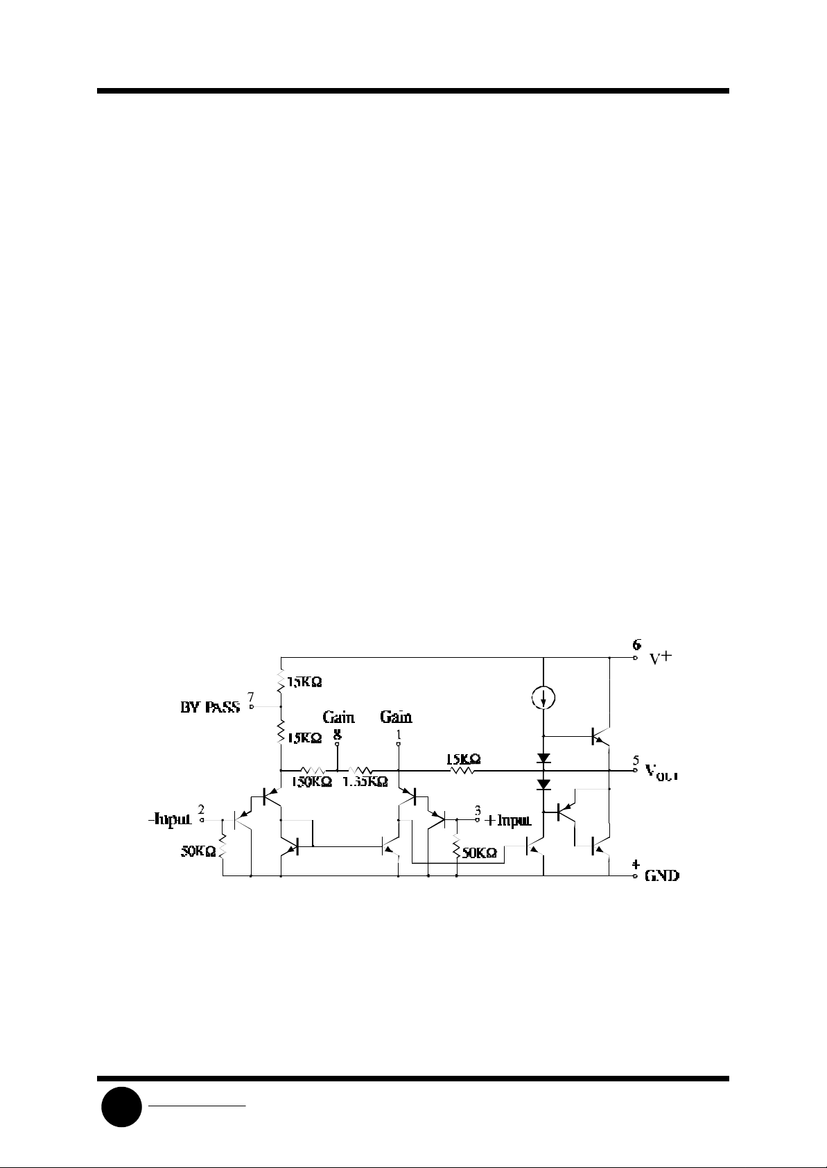
SCHEMATIC DIAGRAM
SL386
INPUT BIASING
The schematic shows that both inputs are biased to
ground with a 50 KΩ resistor. The base current of the
input transistors is about 250 nA, so the inputs are at
at out 12.5 mV when left open. If the dc source
resistance oriving the IL386 is higher than 250 KΩ it
will contribute very little additional offset (about
2.5 mV at the input, 50 mV at the output). If the dc
source resistance is less than 10 KΩ, then shorting
the unused input to ground will keep the offset low
(about 2.5 mV at the input, 50 mV at the output). For
dc source resistances between these values we can
eliminate excess offset by putting a resistor from the
unesed input to ground, equal in value to the dc
source resistance. Of course all affset problems are
eliminated if the input is capacitively coupled.
When using the IL386 with higher gains (by pessing
the 1.35 KΩ resistor between pins 1 and 8) it is
necessary to bypass the unused input, preventing
degradation of gain and possible instabilities. This is
done with a 0.1 µF capacitor or a short to ground
depending on the dc source resistance on the driven
input.
System Logic
SLS
Semiconductor
 Loading...