

Page 1
Semiconductor
Low Power Audio Amplifier
SL34119
The SL34119 is a low power audio amplifier integrated circuit intended
(primarily) for telephone applications, such as in speakerphones. It
provides differential speaker outputs to maximize output swing at low
supply voltages (2.0 volts minimum). Coupling capacitors to the
speaker are not required. Open loop gain is 80 dB, and the closed loop
gain is set with two external resistors. A Chip Disable pin permits
powering down and/or muting the input signal. The SL34119 is
available in a standard 8 pin DIP or a surface mount package.
• Wide Operating Supply Voltage Range (2-16 Volts) - Allows
Telephone Line Powered Applications
• Low Quiescent Supply Current for Battery Powered Applications
• Chip Disable Input to Power Down the IC
• Low Power Down Quiescent Current
• Drives a Wide Range of Speaker Loads (8-100Ω)
• Output Power Exceeds 250 mW with 32Ω Speaker
• Low Total Harmonic Distortion
• Gain Adjustable from <0 dB to >46 dB for Voice Band
• Requires Few External Components
ORDERING INFORMATION
SL34119N Plastic
SL34119D SOIC
TA = -10° to 70° C for
all packages
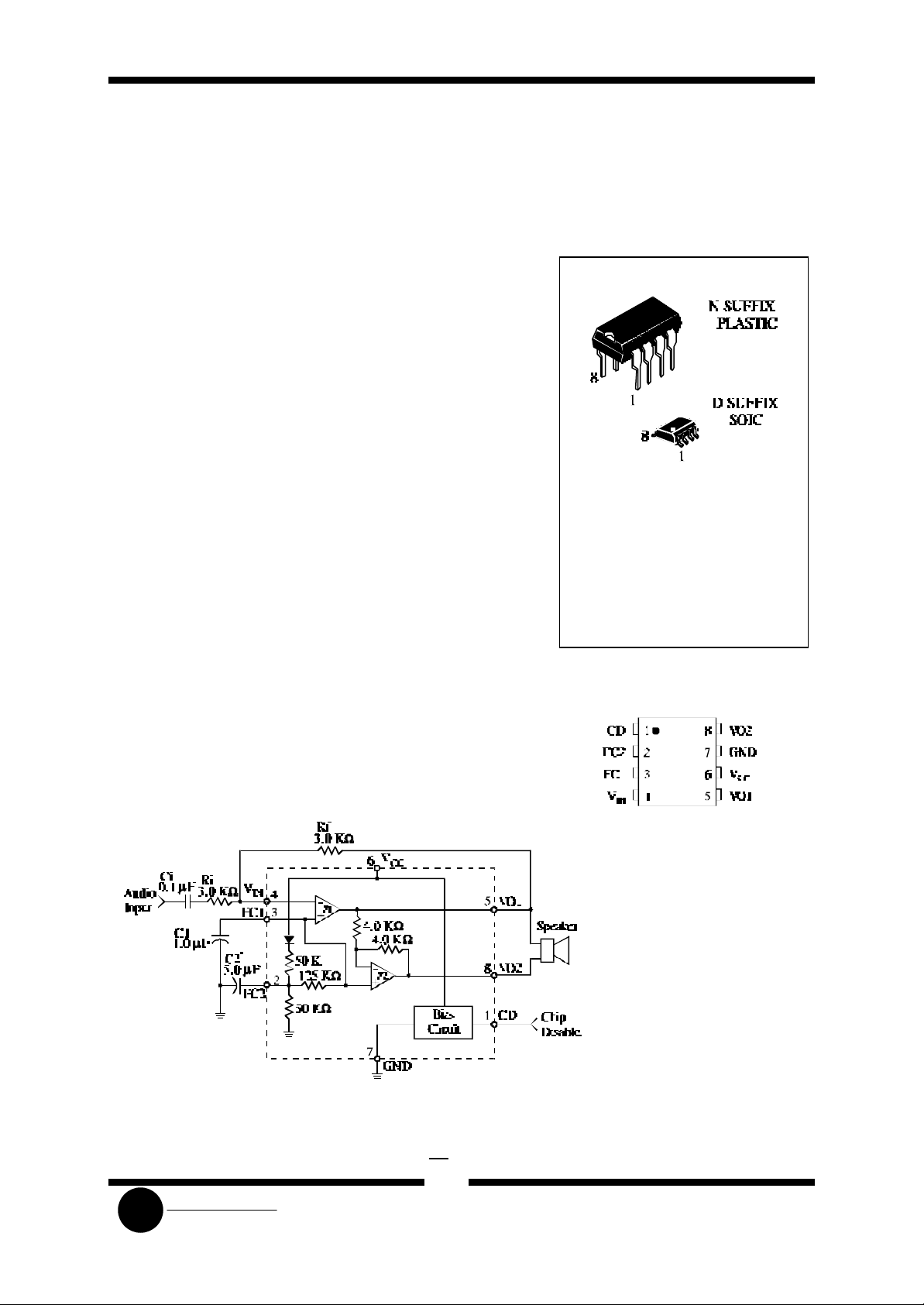
PIN ASSIGNMENT
SLS
SIMPLIFIED BLOCK DIAGRAM
* = Optional
Differential Gain = 2 x
System Logic
R
Ri
f
Page 2
SL34119
Semiconductor
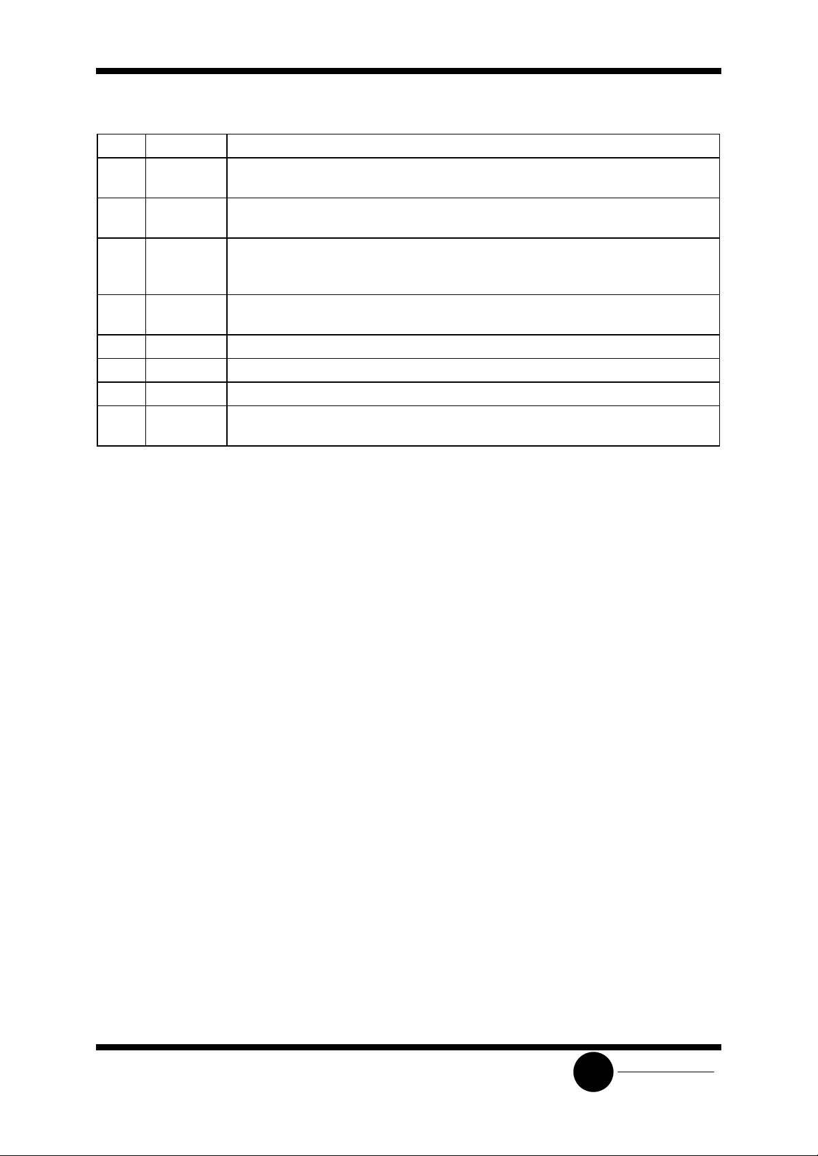
PIN DESCRIPTION
Pin Symbol Description
1 CD Chip Disable - Digital input. A Logic “0” (<0.8 V) sets normal operation. A Logic “1”
(≥2.0 V) sets the power down mode. Input impedance is nominally 90 KΩ.
2 FC2 A capacitor at this pin increases power supply rejection, and affects turn-on time. This
pin can be left open if the capacitor at FC1 is sufficient.
3 FC1 Analog Ground for the amplifiers. A 1.0 µF capacitor at this pin (with a 5.0 µF capacitor
at Pin 2) provides 52 dB of power supply rejection. Turn-on time of the circuit is
affected by the capacitor on this pin. This pin can be used as an alternate input.
4 VIN Amplifier input. The input capacitor and resistor set low frequency rolloff and input
impedance. The feedback resistor is connected to this pin and VO1.
5 VO1 Amplifier Output #1. The dc level is ≈ (VCC - 0.7 V)/2.
6 VCC DC supply voltage (+2.0 to +16 Volts) is applied to this pin.
7 GND Ground pin for the entire circuit.
8 VO2 Amplifier Output #2. This signal is equal in amplitude, but 180° out of phase with that
at VO1. The dc level is ≈ (VCC - 0.7 V)/2.
DESIGN GUIDELINES
GENERAL
The SL34119 is a low power audio amplifier
capable of low voltage operation (VCC = 2.0 V
minimum) such as that encountered in line-powered
speakerphones. The circuit provides a differential
output (VO1-VO2) to the speaker to maximize the
available voltage swing at low voltages. The
differential gain is set by two external resistors. Pins
FC1 and FC2 allow controlling the amount of power
supply and noise rejection, as well as providing
alternate inputs to the amplifiers. The CD pin permits
powering down the IC for muting purposes and to
conserve power.
AMPLIFIERS
Referring to the block diagram, the internal
configuration consists of two identical operational
amplifiers. Amplifier #1 has an open-loop gain of
≥80 dB (at f ≤ 100 Hz), and the closed loop gain is set
by external resistors Rf and Ri. The amplifier is unity
gain stable, and has a unity gain frequency of
approximately 1.5 MHz. In order to adequately cover
the telephone voice band (300-340 Hz), a maximum
closed loop gain of 46 dB is recommended. Amplifier
#2 is internally set to a gain of -1.0 (0 dB).
The outputs of both amplifiers are capable of
sourcing and sinking a peak current of 200 mA. The
outputs can typically swing to within ≈0.4 volts
above ground, and to within ≈1.3 volts below VCC, at
the maximum current. The output dc offset voltage
(VO1-VO2) is primarily a function of the feedback
resistor (Rf), and secondarily due to the amplifiers’
input offset voltages. The input offset voltage of the
two amplifiers will generally be similar for a particular
IC, and therefore nearly cancel each other at the
outputs. Amplifier #1’s bias current, however, flows
out of VIN (Pin 4) and through Rf, forcing VO1 to shift
negative by an amount equal to [Rf x IIB]. VO2 is
shifted positive an equal amount. The output offset
voltage specified in the Electrical Characteristics is
measured with the feedback resistor shown in the
Simplified Block Diagram, and therefore takes into
account the bias current as well as internal offset
voltages of the amplifiers. The bias current is
constant with respect to VCC.
FC1 and FC2
Power supply rejection is provided by the
capacitors (C1 and C2 in the Simplified Block
Diagram) at FC1 and FC2. C2 is somewhat dominant at
low frequencies, while C1 is dominant at high
frequencies. The reguired values of C1 and C2
depend on the conditions of each application. A
SLS
System Logic
Page 3
SL34119
Semiconductor
line powered speakerphone, for example, will require
more filtering than a circuit powered by a well
requlated power supply. The amount of rejection is a
function of the capacitors, and the equivalent
impedance looking into FC1 and FC2 (listed in the
Electrical Characteristics as R
FC1
and R
FC2
).
In addition to providing filtering, C1 and C2 also
affect the turn-on time of the circuit at power-up,
since the two capacitors must change up through the
internal 50 KΩ and 125 KΩ resistors.
CHIP DISABLE
The Chip Disable (Pin 1) can be used to power
down the IC to conserve power, or for muting, or both.
When at a Logic “0” (0 to 0.8 Volts), the IL34119 is
enabled for normal operation. When Pin 1 is at a
Logic “1” (2.0 to VCC Volts), the IC is disabled. If Pin 1
is open, that is equivalent to a Logic “0”, although
good design practice dictates that an input should
never be left open. Input impedance at Pin 1 is a
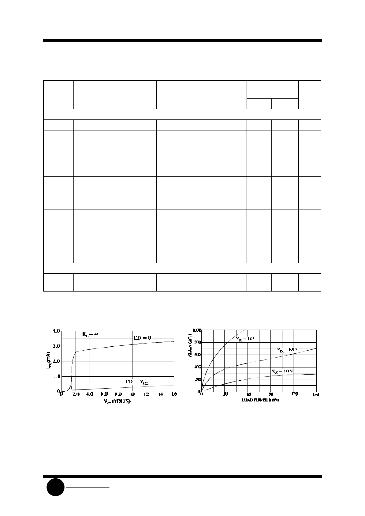
nominal 90 KΩ. The power supply current (when
disabled) is shown in Figure 1.
Muting, defined as the change in differential gain
from normal operation to muted operation, is in excess
of 70 dB. The turn -off time of the audio output, from
the application of the CD signal, is <2.0 µs, and turn
on-time is 12-15 ms. Both times are independent of C1,
C2, and VCC.
When the SL34119 is disabled, the voltages at
FC1 and FC2 do not change as they are powered from
VCC. The outputs, VO1 and VO2, change to a high
impedance condition, removing the signal from the
speaker. If signals from other sources are to be
applied to the outputs (while disabled), they must be
within the range of VCC and Ground.
POWER DISSIPATION
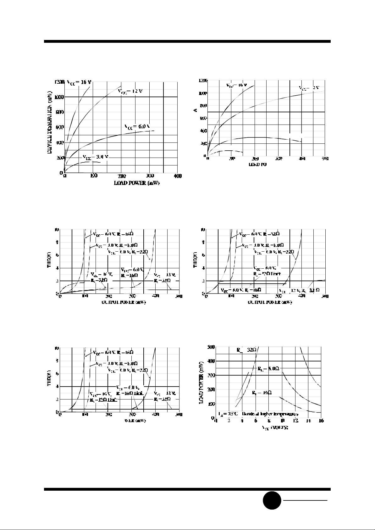
Figures 2-4 indicate the device dissipation (within
the IC) for various combinations of VCC, RL,
MAXIMUM RATINGS*
and load power.The maximum power which can safely
be dissipated within the SL34119 is found from the
following equation:
PD = (140°C - TA)/θJA
where TA is the operating temperature;
and θJA is the package thermal resistance (100°C/W
for the standard DIP package, and 180°C/W for the
surface mount package).
The power dissipated within the SL34119, in a
given application, is found from the following
eguation:
PD = (VCC x ICC) + (I
x VCC) - (RL x I
RMS
RMS
2
).
where ICC is obtained from Figure 1;
and I
is the RMS current at the load;
RMS
and RL is the load resistance.
Figures 2-4, along with Figures 5-7 (distortion
curves), and a peak working load current of ±200 mA,
define the operating range for the IL34119. The
operating range is further defined in terms of
allowable load power in Figure 8 for load of 8.0 Ω,
16 Ω, and 32 Ω. The left (ascending) portion of each
of the three curves is defined by the power level at
which 10% distortion occurs. The center flat portion
of each curve is defined by the maximum output
current capability of the SL34119. The right
(descending) portion of each curve is defined by the
maximum internal power dissipation of the IC at 25°C.
At higher operating be reduced according to the
above equations. Operating the device beyond the
current and junction temperature limits will degrade
long term reliability.
LAYOUT CONSIDERATIONS
Normally a snubber is not needed at the output of
the SL34119, unlike many other audio amplifiers.
However, the PC board layout, stray capacitances,
and the manner in which the speaker wires are
configured, may dictate otherwise. Generally the
speaker wires should be twisted tightly, and be not
more than a few inches in length.
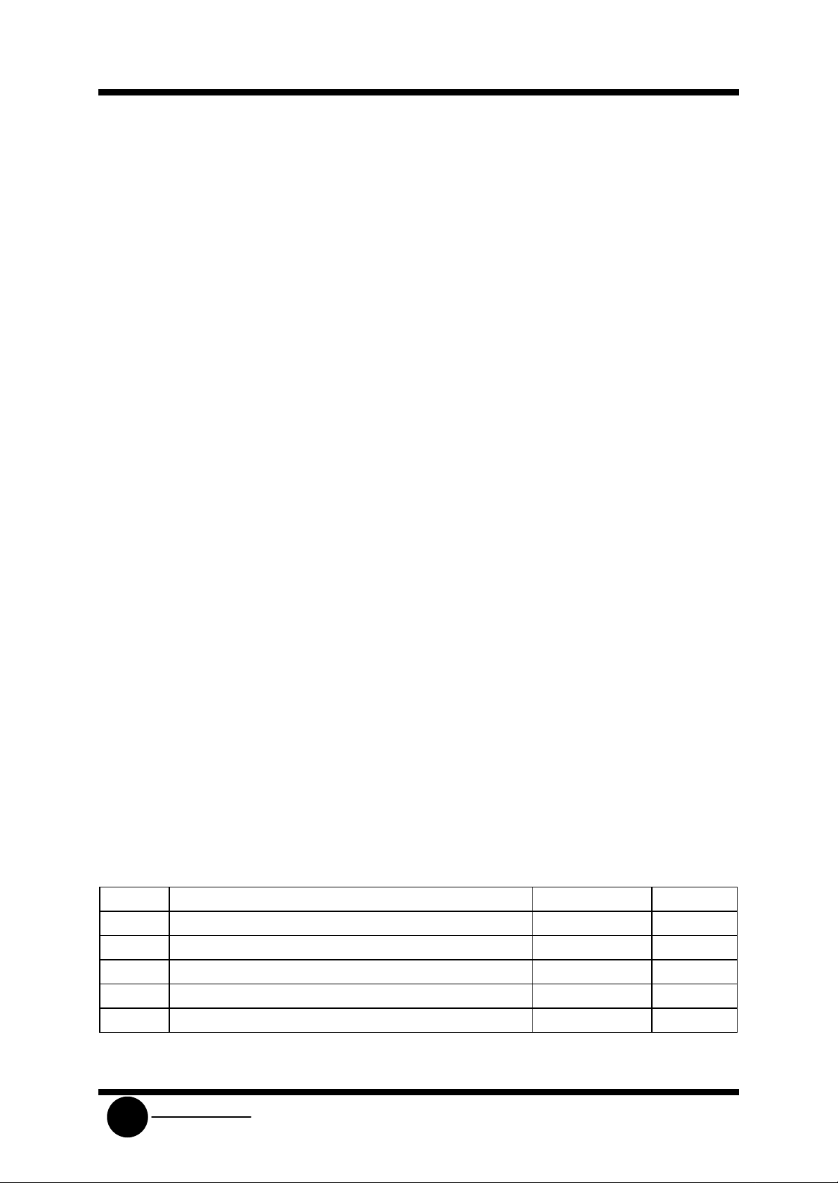
Symbol Parameter Value Unit
VCC Supply Voltage 1.0 to +18 V
I
Maximum Output Current at VO1, VO2 ±250 mA
OUT
VIN MaximumInput Voltage(FC1, FC2, CD, VIN) -1.0 toVCC +1.0 V
VVO Applied Output Voltage to VO1, VO2 when disabled -1.0 toVCC +1.0 V
Tstg Storage Temperature Range -65 to +150 °C
*
Maximum Ratings are those values beyond which damage to the device may occur.
Functional operation should be restricted to the Recommended Operating Conditions.
System Logic
SLS
Page 4
SL34119
Semiconductor
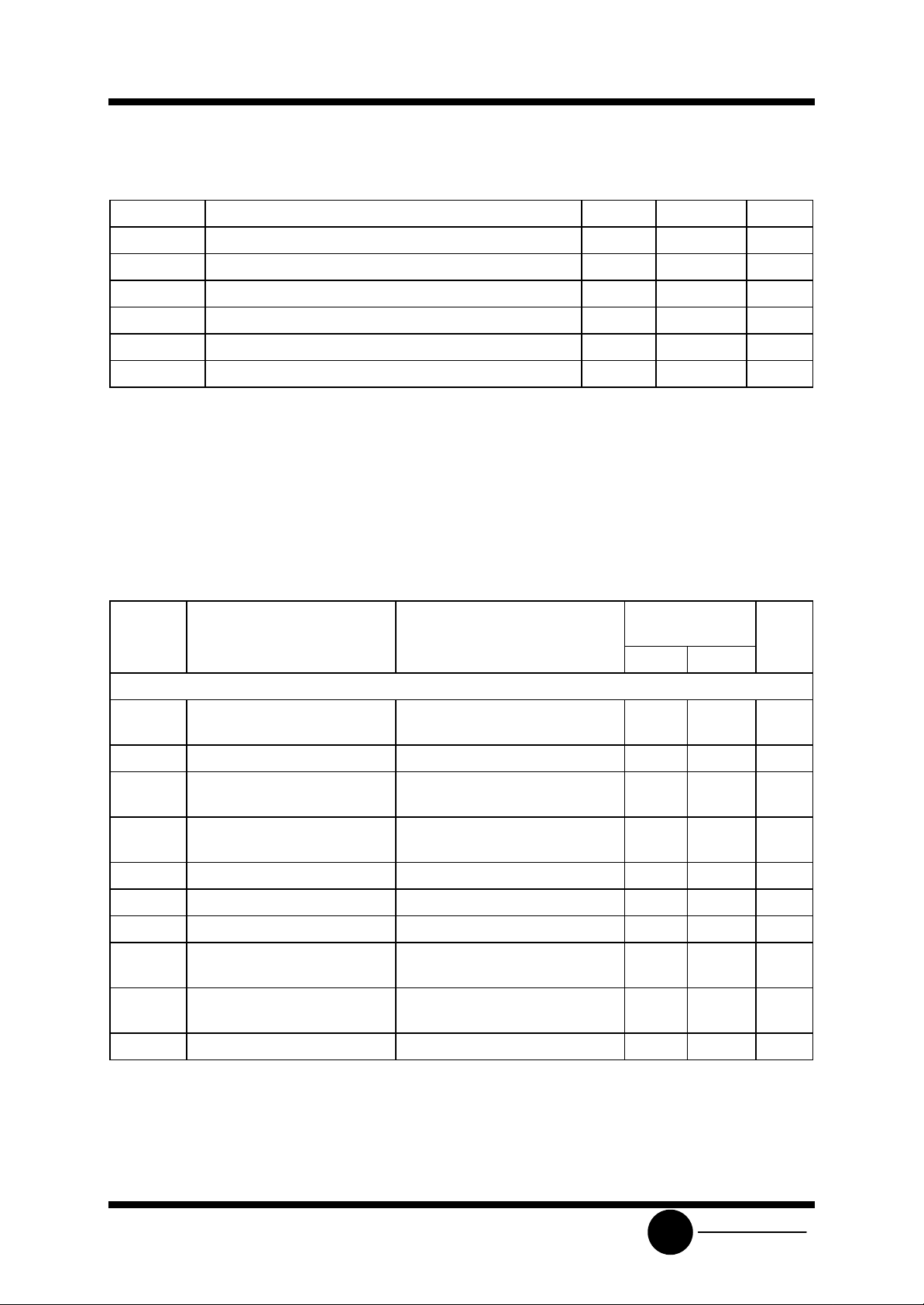
RECOMMENDED OPERATING CONDITIONS
Symbol Parameter Min Max Unit
VCC Supply Voltage 2.0 16 V
RL Load Impedance 8.0 100 Ω
IL Peak Load Current - 200 mA
AVD Differential Gain (5.0 KHz bandwidth) 0 46 dB
VCD Voltage @ CD (Pin 1) 0 VCC V
TA Operating Temperature, All Pakage Types -10 +70 °C
This device contains protection circuitry to guard against damage due to high static voltages or electric
fields. However, precautions must be taken to avoid applications of any voltage higher than maximum rated
voltages to this high-impedance circuit. For proper operation, VIN and V
GND≤(VIN or V
OUT
)≤VCC.
Unused inputs must always be tied to an appropriate logic voltage level (e.g., either GND or VCC).
Unused outputs must be left open.
ELECTRICAL CHARACTERISTICS(T
Symbol
Parameter
= -10 to +70°C, VCD = 0 V)
A
Test Conditions
should be constrained to the range
OUT
Guaranteed
Limits
Unit
Min Max
AMPLIFIERS (DC CHARACTERISTICS)
VO Output DC Level (VO1, VO2) V
=3.0 V, RL =16Ω
CC
0.75 1.75 V
Rf = 75 KΩ
VOH Output High Level I
VOL Output Low Level I
= -75 mA, VCC = 2.0 V 0.5 - V
OUT
= 75 mA,
OUT
- 0.55 V
2.0 V ≤ VCC ≤ 16 V
∆VO Output DC Offset Voltage
(VO1-VO2)
V
=6.0 V, RL =32Ω
CC
Rf = 75 kΩ
-200 200 mV
IIB Input Bias Current @ VIN VCC =6.0 V - 1600 nA
R
Equivalent Resistance @ FC1 VCC = 6.0 V 100 220 KΩ
FC1
R
Equivalent Resistance @ FC2 VCC = 6.0 V 18 40 KΩ
FC2
VIH Minimum High-Level Input
2.0 - V
Voltage
VIL Maximum Low -Level Input
- 0.8 V
Voltage
RCD Input Resistance VCC = VCD = 16 V 50* 175* KΩ
(continued)
SLS
System Logic
Page 5
SL34119
Semiconductor
ELECTRICAL CHARACTERISTICS(T
Symbol
Min Max
AMPLIFIERS (AC CHARACTERISTICS)
ri AC Input Resistance (VIN) 22.5 - MΩ
A
Open Loop Gain (Amplifier #1) f = 100 Hz, VCC = 6.0 V,
VOL1
AV2 Closed Loop Gain (Amplifier
#2)
GBW Gain Bandwidth Product 1.125 - MHz
Parameter
= -10 to +70°C, VCD = 0 V)
A
Test Conditions
V
= 2.65 V
FC2
f = 1.0 KHz, VCC = 6.0 V,
RL=32 Ω
Guaranteed
Limits
60 - dB
-0.35 +0.35 dB
Unit
P
P
OUT12
OUT3
Output Power VCC = 3.0 V, RL = 16 Ω,
THD ≤ 10%, V
VCC = 12.0 V, RL = 100 Ω,
THD ≤ 10%, V
= 1.15 V
FC2
=12 V
FC2
THD Total Harmonic Distortion VCC = 6.0 V, RL = 32 Ω,
f = 1.0 KHz, P
= 125 mW
OUT
PSRR Power Supply Rejection VCC = 6.0 V, ∆VCC = 3.0 V,
C1 =∞, C2 = 0.01 µF
GMT Muting VCC = 6.0 V, f = 1.0 kHz,
CD = 2.0 V
POWER SUPPLY
I
I
CC1
CC2
Maximum Power Supply
Current
*
@25°C
VCC =3.0 V, RL =∞,CD=0.8V
VCC =3.0 V, RL =∞,CD=2.0V
55
400*
-
-
- 5.0 %
35 - dB
50 - dB
-
-
5.0
125
mW
mA
µA
Figure 1. POWER SUPPLY CURRENT
System Logic
SLS
Figure 2. DEVICE DISSIPATION
8.0 Ω LOAD
Page 6
SL34119
Semiconductor
Figure 3. DEVICE DISSIPATION
16 Ω LOAD
Figure 5. DISTORTION versus POWER
f = 1.0 kHz, AVD = 34 dB
Figure 4. DEVICE DISSIPATION
32 Ω LOAD
Figure 6. DISTORTION versus POWER
f = 3.0 kHz, AVD = 34 dB
Figure 7. DISTORTION versus POWER
f = 1, 3.0 kHz, AVD = 12 dB
Figure 8. MAXIMUM ALLOWABLE LOAD POWER
System Logic
SLS
 Loading...