

Page 1
SL2410
System Logic
Semiconductor
SLS
Tone Ringer
The SL2410 is a bipolar integrated circuit designed for telephone bell
replacement.
• Designed for Telephone Bell Replacement
• Low Curent Drain
• Adjustable 2-frequency Tone
• Adjustable Warbling Rate
• Extension Tone Ringer Modules
• Alarms or Other Alerting Devices
• External Triggering or Ringer Disable
• Built-in hysteresis prevents false triggering and rotary dial ‘Chirps’
ORDERING INFORMATION
SL2410N Plastic
SL2410D SOIC
TA = -45° to 65° C
for package
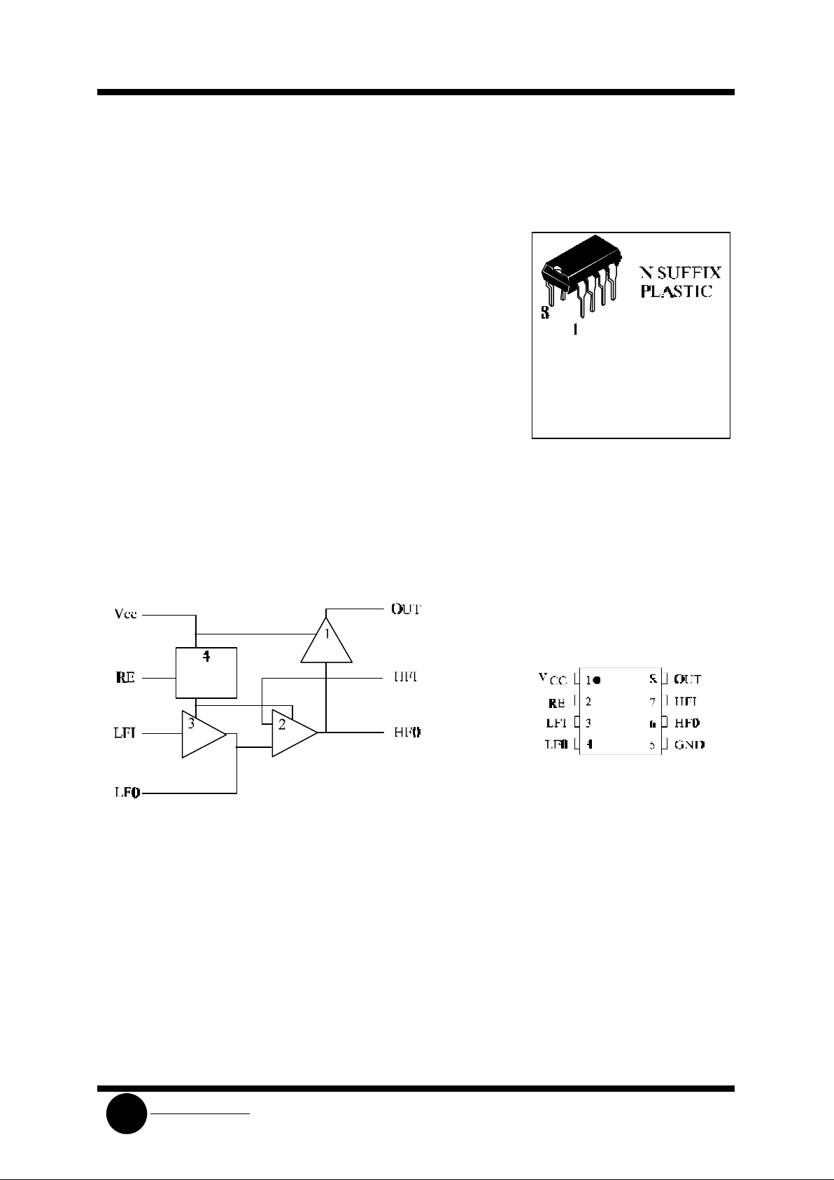
PIN ASSIGNMENT
LOGIC DIAGRAM
PIN 1 = VCC
PIN 5 = GND
1. Output amplifier
2. High frequency oscillator
3. Low frequency oscillator
4. Hysteresis regulator
(Regulator circuit has built-in hysteresis to prevent false
triggering and rotary dial “Chirps”)
Page 2
SL2410
System Logic
Semiconductor
SLS
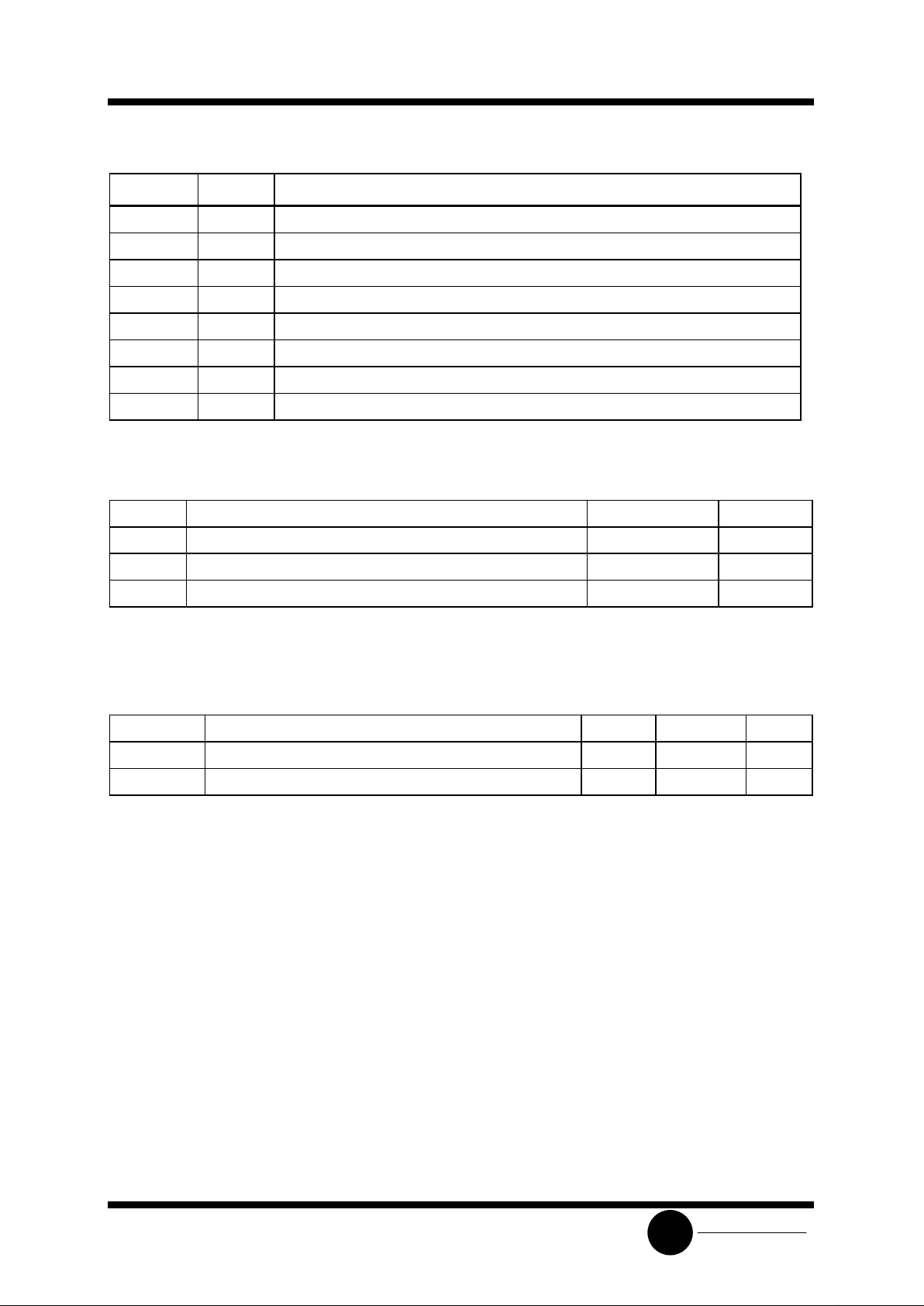
PIN DESCRIPTION
NAME PIN
DESCRIPTION
VCC 1 Positive power supply.
RE 2 Initiation of oscillation start input
LFI 3 Low frequency oscillator input
LF0 4 Low frequency oscillator output
GND 5 Negative power supply
HF0 6 High frequency oscillator output
HFI 7 High frequency oscillator input
OUT 8 Tone output
MAXIMUM RATINGS*
Symbol Parameter Value Unit
VCC DC Supply Voltage (Referenced to GND) to +30.0 V
PD Power Dissipation in Still Air, Plastic DIP 400 mW
Tstg Storage Temperature -65 to +150 °C
*
Maximum Ratings are those values beyond which damage to the device may occur.
Functional operation should be restricted to the Recommended Operating Conditions.
RECOMMENDED OPERATING CONDITIONS
Symbol Parameter Min Max Unit
VCC DC Supply Voltage (Referenced to GND) 13.0 29.0 V
TA Operating Temperature -45 +65 °C
This device contains protection circuitry to guard against damage due to high static voltages or electric
fields. However, precautions must be taken to avoid applications of any voltage higher than maximum rated
voltages to this high-impedance circuit. For proper operation, VIN and V
OUT
should be constrained to the range
GND≤(VIN or V
OUT
)≤VCC.
Unused inputs must always be tied to an appropriate logic voltage level (e.g., either GND or VCC).
Unused outputs must be left open.
Page 3
SL2410
System Logic
Semiconductor
SLS
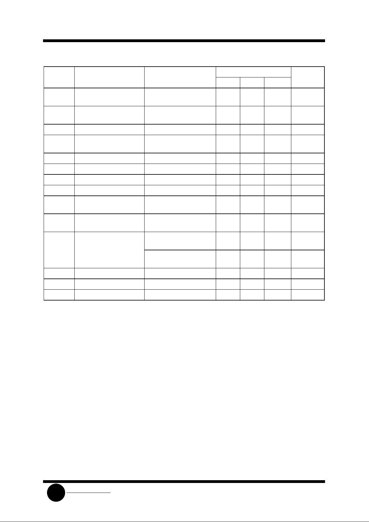
ELECTRICAL CHARACTERISTICS(Voltages Referenced to GND, T
A
= -45 to +65°C)
Guaranteed Limits
Symbol Parameter Test Conditions Min Typ Max Unit
VSI Initiation Supply Voltage
(1)
See Fig. 1 16.8 21.2 V
ISI Initiation Supply Current
(1)
1.4 4.2 mA
V
SUS
Sustaining Voltage (2) See Fig. 1 9.5 12.2 V
I
SUS
Sustaining Current (2) No Load VCC=V
SUS
See Fig. 1
0.7 2.5 mA
VTR Trigger Voltage (3) VCC=15V 8.8 12.2 V
ITR Trigger Current (3,5) VCC=15V 5.0 1000 µA
V
DIS
Disable Voltage (4) VCC=21V - 0.7 V
I
DIS
Disable Current (4) VCC=15V -20 - µA
VOH High-Level Output
Voltage
VCC=21V, IOH=-15mA, Pin
6=6V, Pin 7=GND
16.7 21.0 V
VOL Low-Level Output
Voltage
VCC=21V, IOL=15mA, Pin
6=GND, Pin 7=6V
- 1.8 V
IIN Maximun Input Leakage
Current (Pin 3)
Pin 3=6V,
Pin 4=GND, VCC=21V
- 1.0 µA
(Pin 7) Pin 7=6V,
Pin 6=GND, VCC=21V
- 1.0 µA
fH1 High Frequency 1 R3=191KΩ,C3=6800pF 461 563 Hz
fH2 High Frequency 2 R3=191KΩ,C3=6800pF 576 704 Hz
fL Low Frequency R2=165KΩ, C2=0.47µF 9.0 11.0 Hz
Notes:
1. Initiation supply voltage (VSI) is the supply voltage required to start the tone ringer oscillating.
2. Sustaining voltage (V
SUS
) is the supply voltage required to maintain oscillation.
3. VTR and ITR are the conditions applied to trigger in to start oscillation for V
SUS≤VCC≤VSI
.
4. V
DIS
and I
DIS
are the conditions applied to trigger in to inhibit oscillation for VSI≤VCC.
5. Trigger current must be limited to this value externally.
Page 4
SL2410
System Logic
Semiconductor
SLS
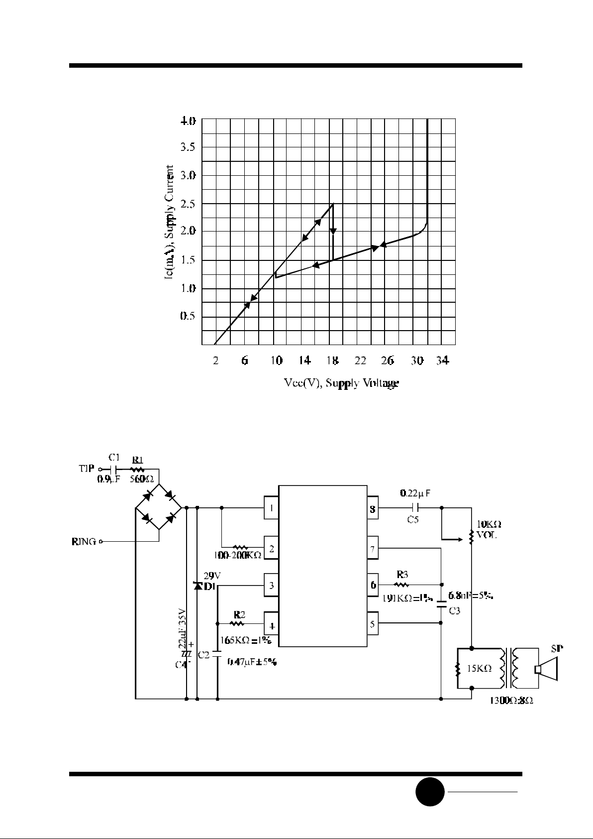
CIRCUIT CURRENT-SUPPLY VOLTAGE (NO LOAD)
Figure 1
APPLICATION CIRCUIT
Figure 2
Page 5
SL2410
System Logic
Semiconductor
SLS
APPLICATION NOTE
The application circuit illustrates the use of the SL2410 devices in typical telephone or extension tone ringer
application.
The AC ringer signal voltage appears across the TIP and RING inputs of the circuit and is attenuated by
capacitor C1 and resistor R1.
C1 also provides isolation from DC voltages (48V) on the exchange line.
After full wave rectification by the bridge diode, the waveform is filtered by capacitor C4 to provide a DC supply
for the tone ringer chip.
As this voltage exceeds the initiation voltage (VSI), oscillation starts.
With the components shown, the ouptut frequency chops between 512(fh1) and 640Hz(fh2) at a 10Hz(fL) rate.
The loudspeaker load is coupled through a 1300Ω to 8Ω ransformer.
The output coupling capacitor C5 is required with transformer coupled loads.
When driving a piezo-ceramic transducer type load, the coupling C5 and transformer (1300Ω:8Ω) are not required.
However, a current limiting resistor is required.
The low frequency oscillator oscillates at a rate (fL) controlled by an external resistor (R2) and capacitor (C2).
The frequency can be determined using the relation fL=1/1.289R2xC2. The high frequency oscillates at a fH1, fH2
controlled by an external resistor (R3) and capacitor (C3). The frequency can be determined using the relation
fH1=1/1.504R3xC3, fH2=1/1.203R3xC3.
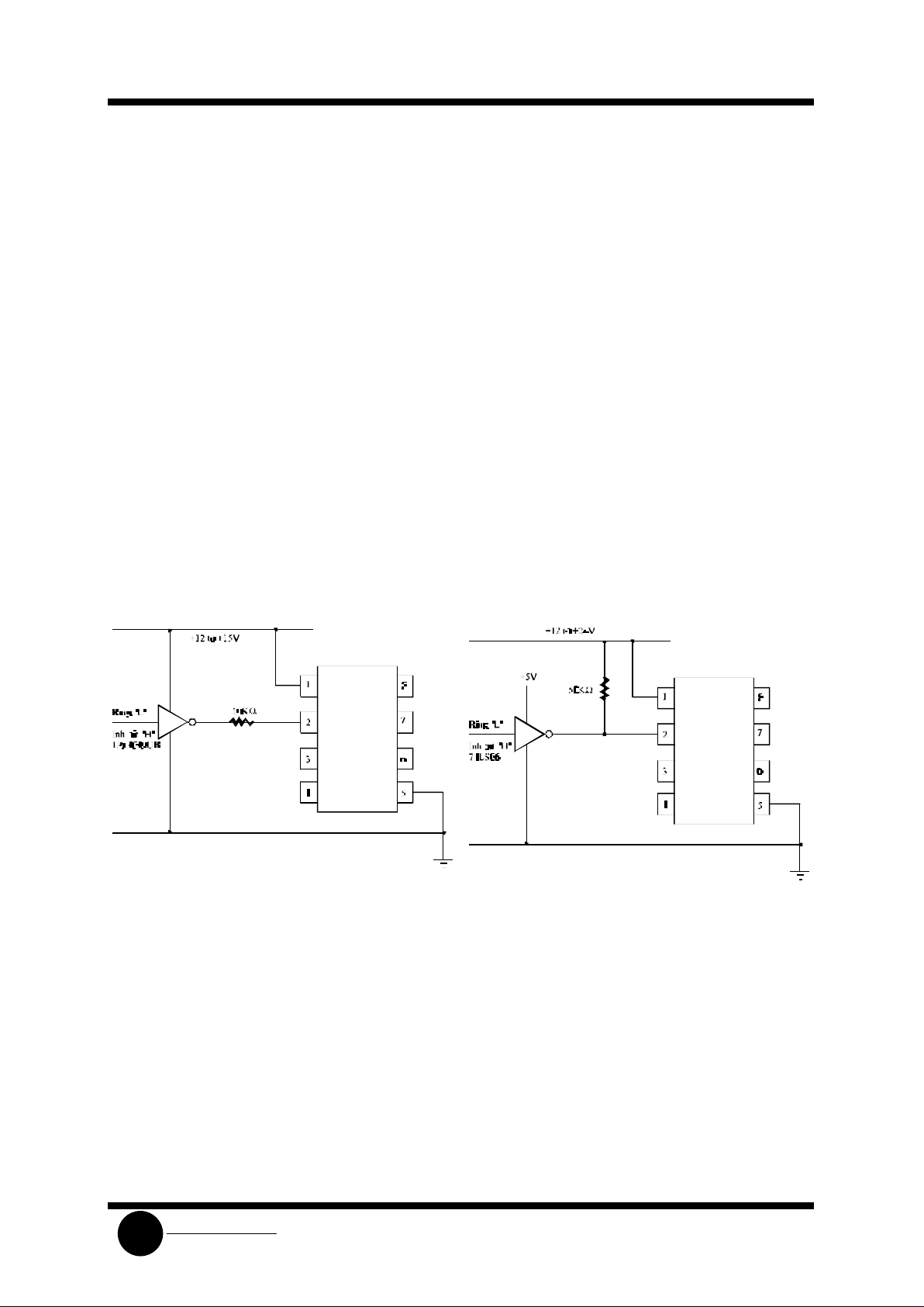
TRIGGERING SL2410 FROM CMOS OR TTL LOGIC
Figure 3
Figure 4
Page 6
SL2410
System Logic
Semiconductor
SLS
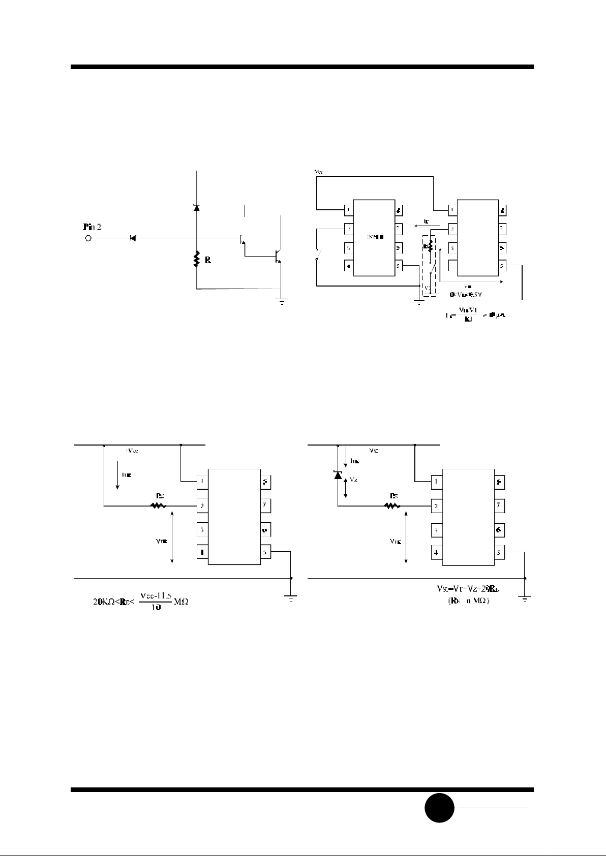
EQUIVALENT CIRCUIT (Pin 2 Input)
INHIVITING OSCILLATION
Figure 5
Figure 6
PROGRAMMING THE SL2410 INITIATION SUPPLY VOLTAGE
Figure 7
Figure 8
 Loading...