

Page 1
FEATURES
■ Single chip full band solution, compatible with
digital and analog transmissions
■ Low noise RF input
■ High input signal handling to eliminate the
requirement for front end AGC
■ Low phase noise local oscillator
■ No prescaler in LO output drive, optimal
architecture for low phase noise applications
■ Low radiation design
■ IF AGC amplifier with dual selectable outputs
■ ESD protection. (Normal ESD handling
procedures should be observed)
ORDERING INFORMATION
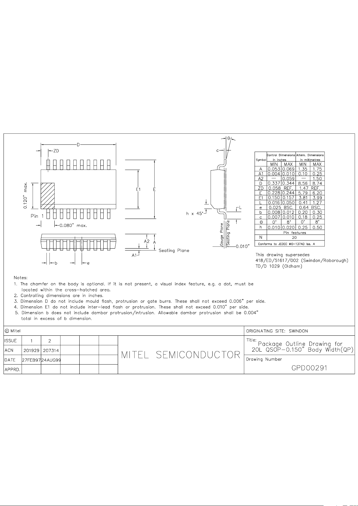
SL2015/KG/QP1S (Tubes)
SL2015/KG/QP1T (Tape and Reel)
The SL2015 is a fully integrated mixer oscillator with output
AGC, intended primarily for application in satellite tuners,
where it downconverts the first high IF from the outdoor unit to
the second IF for data demodulation.
The device contains a low noise RF input amplifier and
mixer functioning to 2.15GHz, an integrated low phase noise
local oscillator and an AGC IF output buffer amplifier. The IF
signal is available at one of two outputs selected by the IF-OPSEL input.
The signal handling of the SL2015 is sufficient to greatly
simplify or remove the requirement for input AGC with
appropriate image filtering in full band systems, or to remove
the requirement for band limit filtering with appropriate AGC
in half band systems.
APPLICATIONS
■ Satellite tuners
■ Communications systems
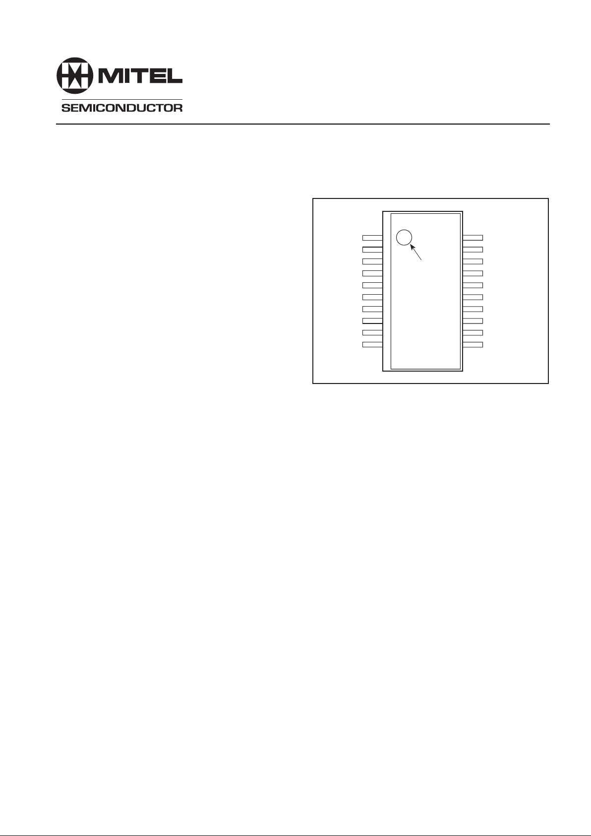
PIN 1
REF. SPOT
Fig.1 Pin connections - top view
V
EE
V
EE
-RF
RF INPUTB
RF INPUT
V
CC
-RF
VCC-LO
TANK
TANKB
V
EE
-LO
IF-OP-SEL
AGC CONTROL
IF OUTPUT1
IF OUTPUT1B
V
CC
-IF
LO OUTPUT
LO OUTPUTB
V
EE
-IF
IF OUTPUT2B
V
EE
IF OUTPUT2
QP20
SL2015
Full Band Satellite Tuner
Advance Information
Supersedes April 1997 version, DS4548 - 2.1 DS4593 - 3.2 February 1998
Page 2
2
SL2015
QUICK REFERENCE DATA
Characteristic Units
RF input noise figure 16 dB
Maximum conversion gain 33 dB
Minimum conversion gain -5 dB
IF1 and IF2 output gain match 2 dB
IP3
2T
input referred at minimum conversion gain +3 dBm
IP22T input referred at minimum conversion gain +17 dBm
LO phase noise at 10kHz -75 dBc/Hz
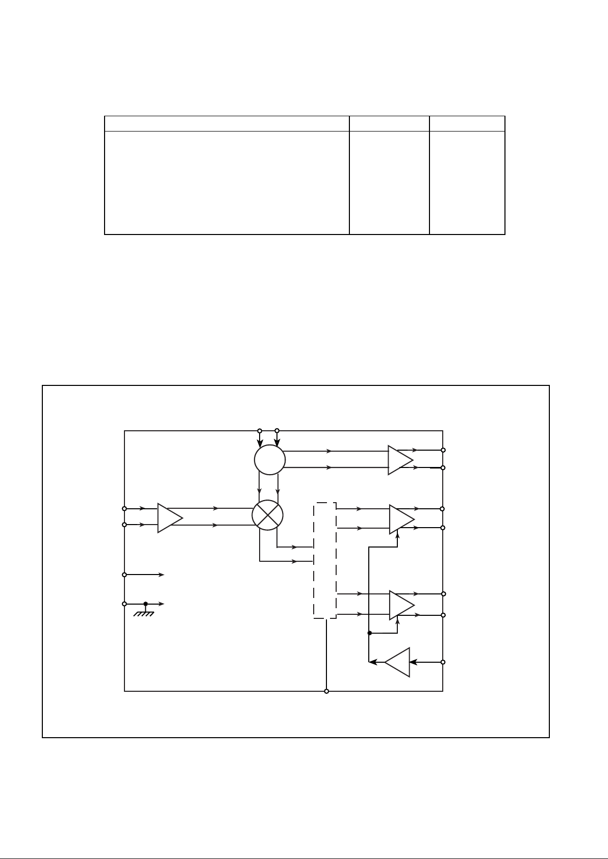
Fig. 2 Block diagram
TANKB
TANK
8
7
16
15
LO OUTPUT
LO OUTPUTB
19
18
IF OUTPUT1
IF OUTPUT1B
13
12
IF OUTPUT2
IF OUTPUT2B
20
AGC CONTROL
10
IF-OP-SEL
3
4
RF INPUTB
RF INPUT
5,6,17
1,2,9,11,14
V
CC
V
EE
Page 3
3
SL2015
The SL2015 is a downconverter mixer oscillator with an
output AGC amplifier, when used with appropriate external
varactor tuned oscillator sustaining network performs the first
IF tuning function for a full band satellite receiver system. A
block diagram is contained in Fig. 2.
In application the RF input of the device is interfaced
through appropriate impedance matching to the first IF
signal, which is downlinked from the outdoor unit at typically
950-2150MHz. The RF input preamplifier of the device is
designed for low noise figure and for low distortion so
eliminating the requirement for RF AGC. The preamplifier
also provides gain to the mixer section and back isolation from
the local oscillator section.
The output of the preamplifier is fed to the mixer section
where the RF signal is mixed with the local oscillator
frequency, which is generated by an on-board oscillator. The
oscillator block uses an external tunable sustaining network
and is optimised for low phase noise. This section also
contains a buffer drive whose outputs can be used to
frequency lock the LO carrier to the required channel.
Signals from the mixer are fed to the AGC IF amplifier,
which gives an overall conversion gain programmable from
-10 to +30dB. The output of this stage can be switched to one
of two outputs to facilitate IF processing.
FUNCTIONAL DESCRIPTION
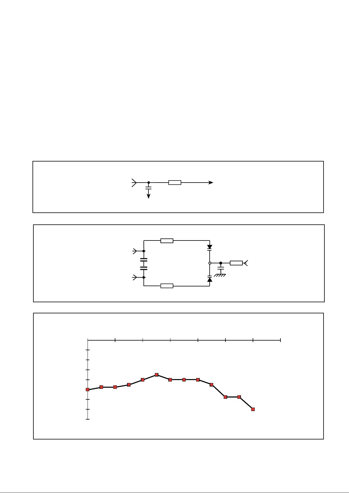
Fig. 3 RF input matching network
Fig. 4 VCO application circuit
6.2nH
TO DEVICE
0.7pF
6mm STRIPLINE
Fig. 5 LO phase noise variation with frequency (typical)
2 x 1T379
10kΩ
Vcnt
0.75p
TANK
TANKB
0.75p
6mm STRIPLINE
SL2015 phase noise
-78.00
-76.00
-74.00
-72.00
-70.00
-68.00
-66.00
-64.00
-62.00
1400 1600 1800 2000 2200 2400 2600 2800
LO frequency MHz
Phase noise dBc/Hz @10kHz
LO frequency MHz
Lo frequency MHz
SL2015 phase noise
Page 4
4
SL2015
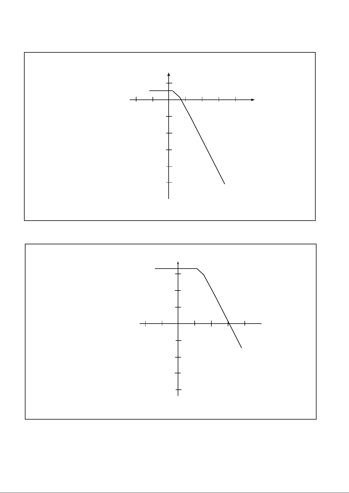
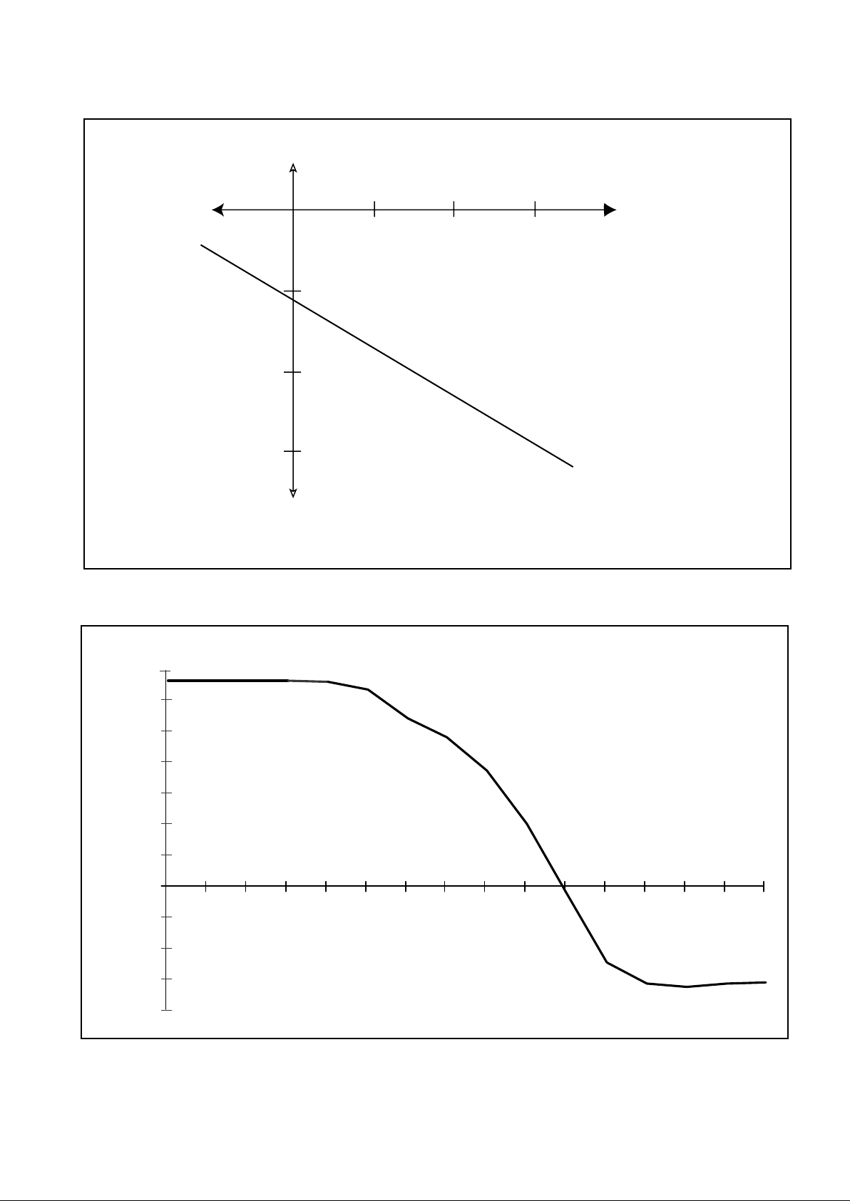
Fig. 6 IP3 variation with gain setting (minimum)
-20 -10 10 20
30 40
-5
-10
-15
-20
-25
IP3 (dBm)
Conversion gain
(dB)
+5
Applies for a constant IF output level of -14dBm
Applies for a constant IF output level of -14dBm
-20 -10 10 20
30 40
-5
-10
-15
-20
+15
+10
+5
IP2 (dBm)
Fig. 7 IP2 variation with gain setting (minimum)
Page 5
5
SL2015
Fig. 8 P1dB with gain setting (typical)
-10
-20
-30
+10
+30
+20
X
X
X
0
-10
RF input level at P1dB (dBm)
Gain setting (dB)
AGC voltage (V)
Conversion gain (dB)
-20
-15
-10
-5
0
5
10
15
20
25
30
1.2
1.4
1.6
1.8 2
2.2 2.4 2.6
2.8 3
3.2 3.4 3.6 3.8
4
35
Fig.9 Gain variation with AGC voltage (typical)
Page 6
6
SL2015
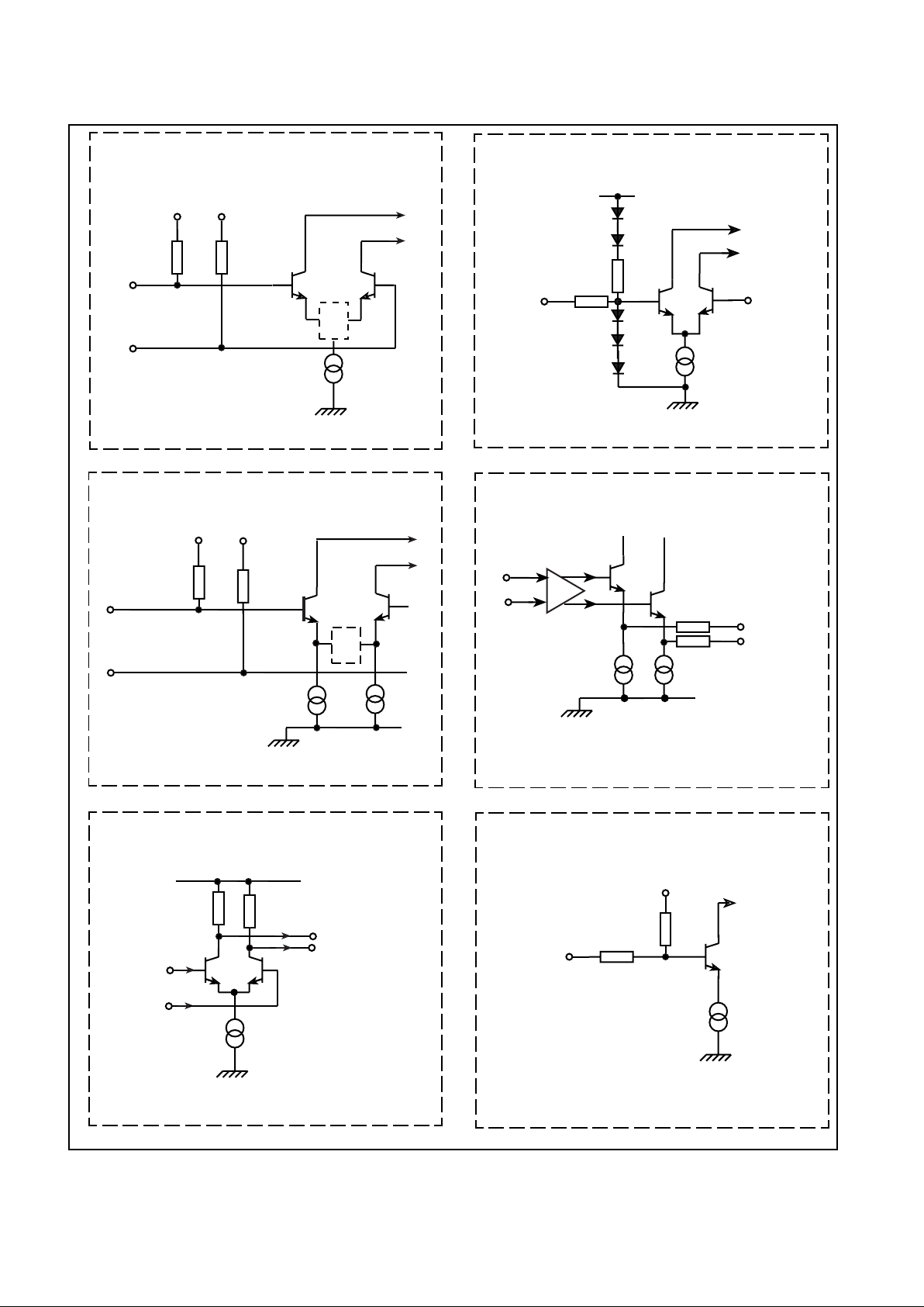
RF inputs IF output select input
Local oscillator inputs
IF outputs
LO buffer drive
AGC input
LO OUTPUT
LO OUTPUTB
V
cc
Fig. 10 Input/output interface circuits
V
REF4
AGC
12K
CONTROL
2K
V
REF 1
300 300
RF INPUTS
V
REF 3
V
cc
IF-OP-SEL
OUTPUT
50
50
OUTPUTB
V
REF 2
1K 1K
TANK
TANKB
Page 7

7
SL2015
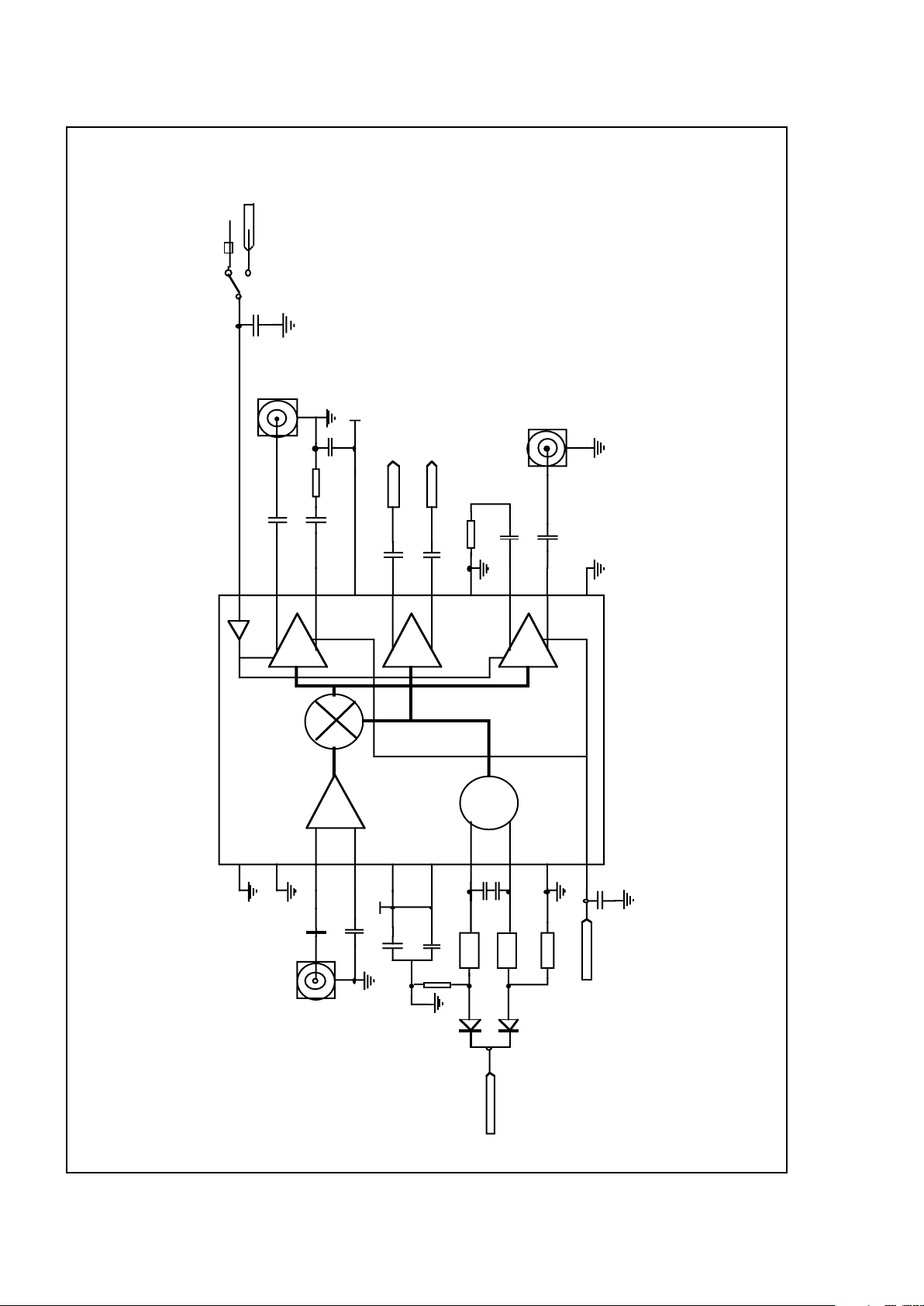
SL2015 Evaluation Board
This board has been created to show the operation of the
SL2015 mixer/oscillator together with the SP5659 low phase
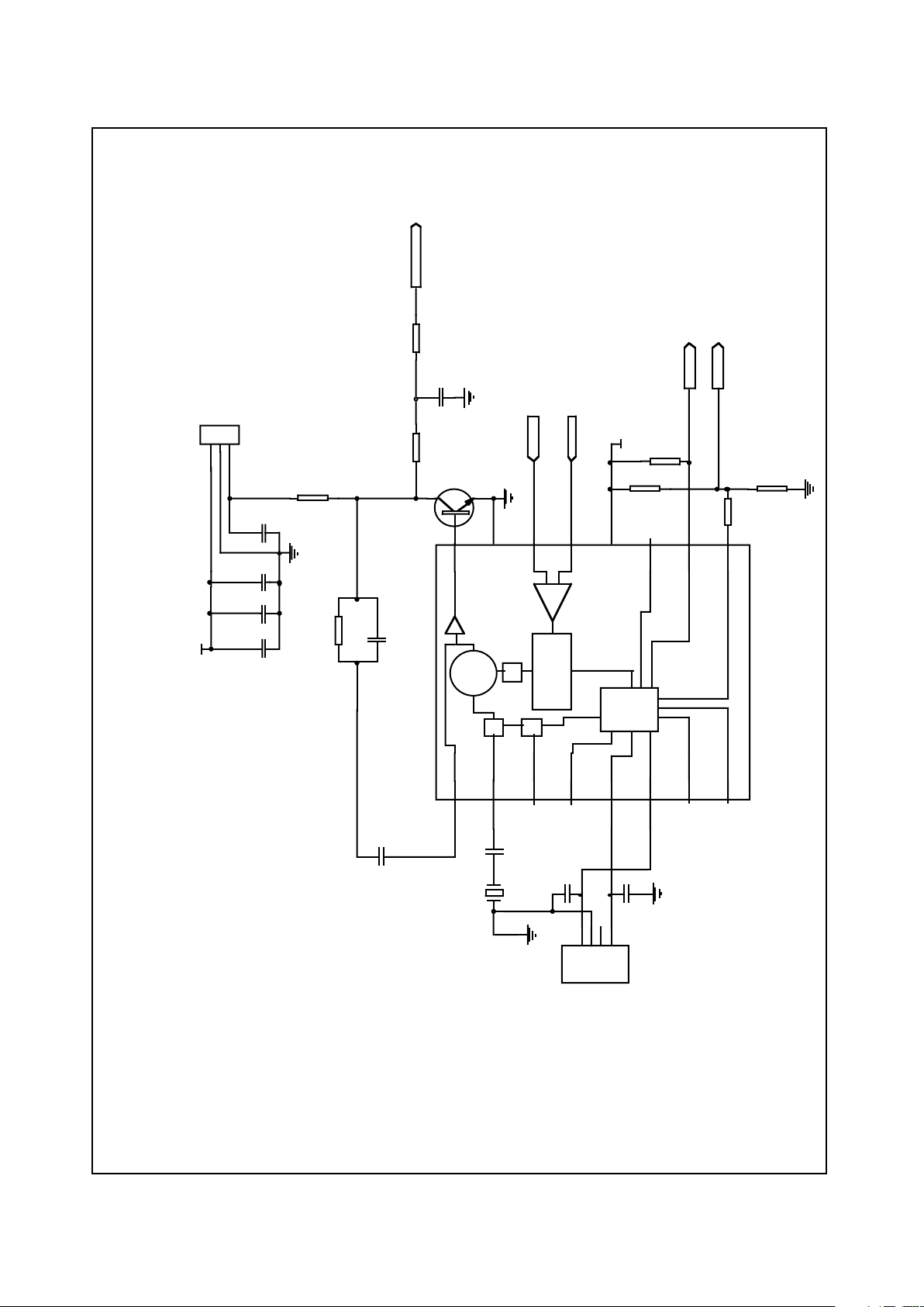
noise synthesiser. Schematics for the board are shown in
Figs. 11a and 11b.
In a real system, the IF output would be fed to a SAW filter
then onto either an FM demodulator such as the SL1466, or an
IQ downconverter such as the SL1710 or SL1711. Control of
the AGC would be via a loop, which should be set up to ensure
that the SL1466, SL1710 or other IF chip receives the correct
level for optimum performance.
For full evaluation, 30V and 5V supplies are necessary,
together with I2C data, RF signal sources and test equipment.
Supplies
The board must be provided with the following supplies:
a) 5V for the SL2015 and SP5659 and 30V for the varactor
line.
The supply connector is a 3 pin 0.1" pitch pin header. The
centre pin of the connector is GND.
I2C Bus connections
b) The board is provided with an RJ11 I2C bus connector
which feeds directly to the SP5659 synthesiser.
This connects to a standard 6-way connector cable which
is supplied with the I
2
C/3-wire bus interface box.
Input and Output connections
The board is provided with the following connectors:
a) RF I/P SMA connector (SMA1) which is AC coupled to the
RF input of the SL2015.
b) IF OUT 1 (SMA2) and IF OUT 2 (SMA5). These outputs
may be selected by switching port P0 on the SP5659.
The standard IF output frequencies used are typically
402.75MHz or 479.5MHz. Either IF output may be connected
directly to 50Ω test equipment such as a spectrum analyser.
Details of programming the SL2015 are included below.
Programming of SP5659 Synthesiser
The SP5659 synthesiser is used to set the frequency of the
SL2015 VCO. Since high sided mixing is normally employed
in satellite tuners, the VCO should be set to the IF above the
wanted input channel.
Example: To mix a wanted channel at 1020.5MHz down
to 479.5MHz.
The synthesiser must be programmed to 1020.5MHz +
479.5MHz = 1500MHz.
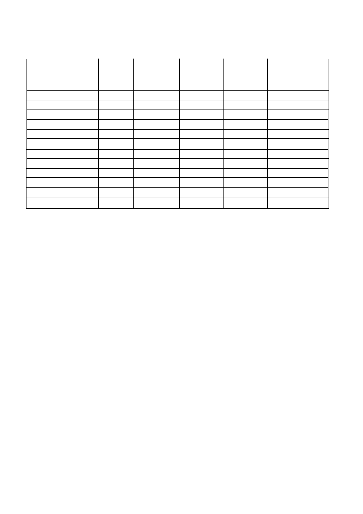
Send I2C data C2 0B B8 93 40 to the SP5659. See Table
1 for example I
2
C codes.
C2 is the address byte (byte 1).
0B B8 is the programmable divider information (bytes 2 and 3).
(i.e. 1500MHz / 500kHz = 3000 = 0BB8Hex)
93 is the programmable and reference divider information
(byte 4). This will enable the prescaler and program the
reference divider to a divide by 16 mode giving a 250kHz
phase comparator frequency with a 500kHz step size when a
4MHz crystal is used.
40 is charge pump and port control data (byte 5).
The code 40 will set the charge pump current to 260uA. All
ports will be switched off.
If it is required to use the SP5659 (for VCO < 2GHz) with the
prescaler disabled it is recommended that data is initially sent
to enable the prescaler. This will avoid a potential 'lock out'
situation arising when the LO frequency is greater than 2GHz.
Links and Switches
The board is provided with the following:
AGC SELECT switch
This switches between programmable control of the
SL2015 AGC, via port P1 of the SP5659, or direct control via
the pin TP1, EXTERNAL AGC VOLTAGE.
In normal application , the AGC will be controlled via a loop,
such that the IF chip which follows is fed with the desired input
level.
Page 8
8
SL2015
Required SL2015 VCO Byte 1 Byte2 Byte 3 Byte 4 Byte 5
Frequency (MHz) Address Prog Divider Prog Divider Prog Divider Charge Pump
8 MSB's 8 LSB's /Reference and Port
Divider Control
1500 C2 0B B8 93 40
1600 C2 0C 80 93 40
1700 C2 0D 48 93 40
1800 C2 0E 10 93 40
1900 C2 0E D8 93 40
2000 C2 0F A0 93 40
2100 C2 10 68 93 40
2200 C2 11 30 93 40
2300 C2 11 F8 93 40
2400 C2 12 C0 93 40
Bottom of Band C2 XX XX 93 11
Top of Band C2 XX XX 93 10
Codes above are for Fcomp = 250kHz, prescaler enabled, giving Fstep = 500kHz.
X = Don't care
Table 1. Example I2C Hex codes for SP5659 synthesiser
Switching of SL2015 IF outputs
Port P0 is used to select the IF ouputs.
When Port P0 is OFF, IF output 1 is selected.
When Port P0 is ON, IF output 2 is selected.
Switching of SL2015 AGC
Port P1 is used to program the AGC gain.
When Port P1 is OFF, AGC is set to 4V (minimum gain).
When Port P1 is ON, the AGC is set to 1V (maximum gain).
SL2015 Operation
The SL2015 is a downconverter mixer oscillator with an
AGC amplifier, which when used with appropriate external
varactor tuned oscillator sustaining network performs the first
IF tuning function for a full band satellite receiver system.
In application the RF input of the device is interfaced
through appropriate impedance matching to the first IF signal,
which is down linked from the outdoor unit at typically 9502150MHz. The RF input preamplifier of the device is designed
for low noise figure and for low distortion so eliminating the
requirement for RF AGC. The preamplifier also provides gain
to the mixer section and back isolation from the local oscillator
section.
The output of the preamplifier is fed to the mixer section
where the RF signal is mixed with the local oscillator
frequency, which is generated by an on board oscillator. The
on board oscillator uses an external tuneable sustaining
network and is optimised for low phase noise. This section
also contains a buffer drive whose outputs can be used to
frequency lock the LO carrier to the required channel.
Signals from the mixer are then fed to the AGC IF amplifier,
which gives an overall conversion gain programmable from
-10 to +30 dB. The output of this stage can be switched to one
of two outputs to facilitate IF processing.
The SL2015 will mix an RF input signal from 950MHz 2150MHz with its own local oscillator, and produce an IF signal
typically at 402.75MHz or 479.5MHz.
The device has a number of features, which may be either
programmable via a synthesiser and operated as part of a
dynamic AGC loop, or hardwired into a fixed mode.
There are a variety of parameters which can be measured
using this evaluation board.
Use with external oscillator.
For applications that require extremely good phase noise,
typically >-75dBc @ 10kHz across the band, it is
recommended that the SL2017 together with an external local
oscillator is used.
The SL2017 is functionally equivalent to the SL2015,
however the tank inputs have been modified to act as a buffer
to an external VCO. Further details of this application are
shown in the SL2017 Datasheet.
Page 9

9
SL2015
Measurement of Phase Noise.
This is best measured by looking at the IF output of the
SL2015. The IF should be fed to a spectrum analyser, where
it can be interpreted.
There are two common methods of doing this:
a) using phase noise analysis software (such a HP85671A
phase noise program)
b) direct measurement of the noise floor at the chosen offset
frequency, and conversion to a dBc/Hz figure.
Since method a) will depend on the software used, a
description of method b) will be given only.
To measure phase noise at 10kHz offset:
a) tune the centre frequency of the spectrum analyer to the
IF - e.g. 479.5MHz
b) Set the span initially wide (10MHz or greater). Gradually
reduce this until it is set to 50kHz or less, taking care to ensure
that the centre frequency of the display matches the IF peak.
c) perform a peak search
d) set marker delta to 10kHz
e) set video averaging ON to ensure that a representative
measurement of the noise floor at the chosen offset frequency
is made.
f) record the level of noise at the 10kHz offset compared to
the peak IF level (in dBc).
Measurement of Conversion Gain
(from a 50Ω source)
a) Connect an RF signal generator to the RF input to the
SL2015.
b) Connect an IF output to a spectrum analyser.
c) Feed the SL2015 with the appropriate signal level,
depending on AGC setting, required output, etc.
d) Note the relative difference in the input and IF level in dB.
This is the conversion gain of the device.
For increased accuracy, the input signal level should also
be checked with a spectrum analyser, since any level
measurement errors that exist within the analyser will then be
relative, rather than literal.
The AGC voltage may be varied and conversion gain
measured at different AGC voltages.
Care must be taken to ensure that the LO is stable, since any
instability will reduce the averaged peak LO value, thus giving
a falsely low phase noise reading.
g) convert the measured reading to a 1Hz bandwidth.
e.g. A measured phase noise of -50dBc/1kHz bandwidth
(RBW of 1kHz) corresponds to -80dBc/Hz.
Since noise floor must be reduced by the ratio of the two
bandwidths
i.e. 10 log 1kHz/1Hz = 30dB.
Page 10

10
SL2015
e) The difference in level in dB between the fundamentals and
the 3rd order products is the IM3 of the device.
f) IP3 may be calculated from the above reading as follows:
IP3 = RF input level + IM3/2.
This level is usually referred to the input.
e.g.
Assuming a measured IM3 of 44dB, and with an input level of
-19dBm,
IP3 = 44/2 + -19dBm = +3dBm
In a 50Ω system, this may be converted to dBuV by adding 107
to the value calculated since 0dBm = 107dBµV.
i.e. +3dBm = 110dBuV.
This is known as the input referred IP3 of the device.
If you experience any difficulties with this board, or require
further help, please contact Robert Marsh on 01793 518234
or Fred Herman on 01793 518423. The fax number is 01793
518411.
The in-band ones are listed below:
fd = flo - (2 x f1 - f2)
fc = flo - (2 x f2 - f1)
fd = 1430MHz - (2 x 950MHz - 951MHz) = 481MHz
fc = 1430MHz - (2 x 951MHz - 950MHz) = 478MHz
fa fb
fc
fd
fundamentals
3rd order product
3rd order product
Measurement of IM3 and IP3
a) Input two signal tones from RF generators. The level of
these should be adjusted so that the device sees an input
signal level of -19dBm from each tone.
Program the local oscillator so that both tones are mixed down
to the IF (approx).
b) Adjust the AGC so that the device gives an overall
conversion gain of +5dB.
c) Connect a spectrum analyser to the selected IF output of
the device.
d) Measure the relative levels of the down converter signals
and the 3rd order products (see diag overleaf).
Two input signals are used:
f1 = 950MHz
f2 = 951MHz
The local oscillator flo is tuned to 1430MHz.
This gives the following at the IF output:
fa = 1430MHz - 950MHz = 480MHz
fb = 1430MHz - 951MHz = 479MHz
Mixing products are also produced in the front end. These
are then downconverted by the mixer.
Page 11
11
SL2015
1
2
3
4
5
P3
7
P2
8
P1
9
P0
10
ADC
11
VCC
12
13
14
VEE
15
16
6
RF Input
RF Input
Xtal
Charge Pump
Drive Output
SDA
SCL
Ref/Comp
Address
I2C Bus
Interface
Programmable
Divider
Phase
Comp
IC2
SP5659
C32
68pF
R7
13K
T1
BCW31
R8
22K
123
J1
POWER CONNECTOR
5V
R9
16K
R10
47K
C39
2n2F
C41
4u7F
C36
100pF
C33
100nF
+5V
+30V
C34
100nF
5V
Varactor line
RF
RF B
R16
10K
IF OP SEL
R13
220R
R15
1K
R14
4K
AGC
C31
15nF
SDA5
3
5V0
4
GND
5
SCL5
6
J3
I2C BUS
C38
100pF
C37
100pF
C30
18pF
X1
4MHz
GND
Fig. 11a Evaluation board schematic PLL section
Page 12
12
SL2015
Fig. 11b Evaluation board schematic SL2015 Section
Vee1Vee RF
2
3
4
Vcc RF
5
7
8
13
Vee IF
14
15
16
Vcc IF
17
18
19
20
Vcc LO
6
Vee LO
9
10
Vee
11
12
RF IP B
RF IP
TANK
TANKB
IF OUT2B
IF OUT2
LO OP2
LO OP
IF OUT1
IF OUT1B
AGC
NOTE: DIFFERENTIAL SIGNALS ARE SHOWN AS THICK LINES
IF OP SEL
OSC
IC1
SL2015
C1
1nF
C7
1nF
RF
C3
1nF
C9
1nF
5V
C4
100pFC5100pF
C6
100pF
5V
C2
1nF
C8
1nF
SMA5
IF OUT 2B
SMA2
IF OUT 1
IF OP SEL
C10
1nF
SMA1
RF INPUT
RF B
C11
1nF
STRIP 6MM
IT379BB835
IT379BB835
VARACTOR LINE
D1
D2
R2
1M
R1
1M
L1
STRIP 6MM
L2
S1
AGC SEL
C13
1nF
C14
1nF
R3
50R
R4
50R
C12
0p75F
0p75F
EXTERNAL AGC
VOLTAGE
TPI
AGC
D1
IT379
D2
IT379
Page 13
13
SL2015
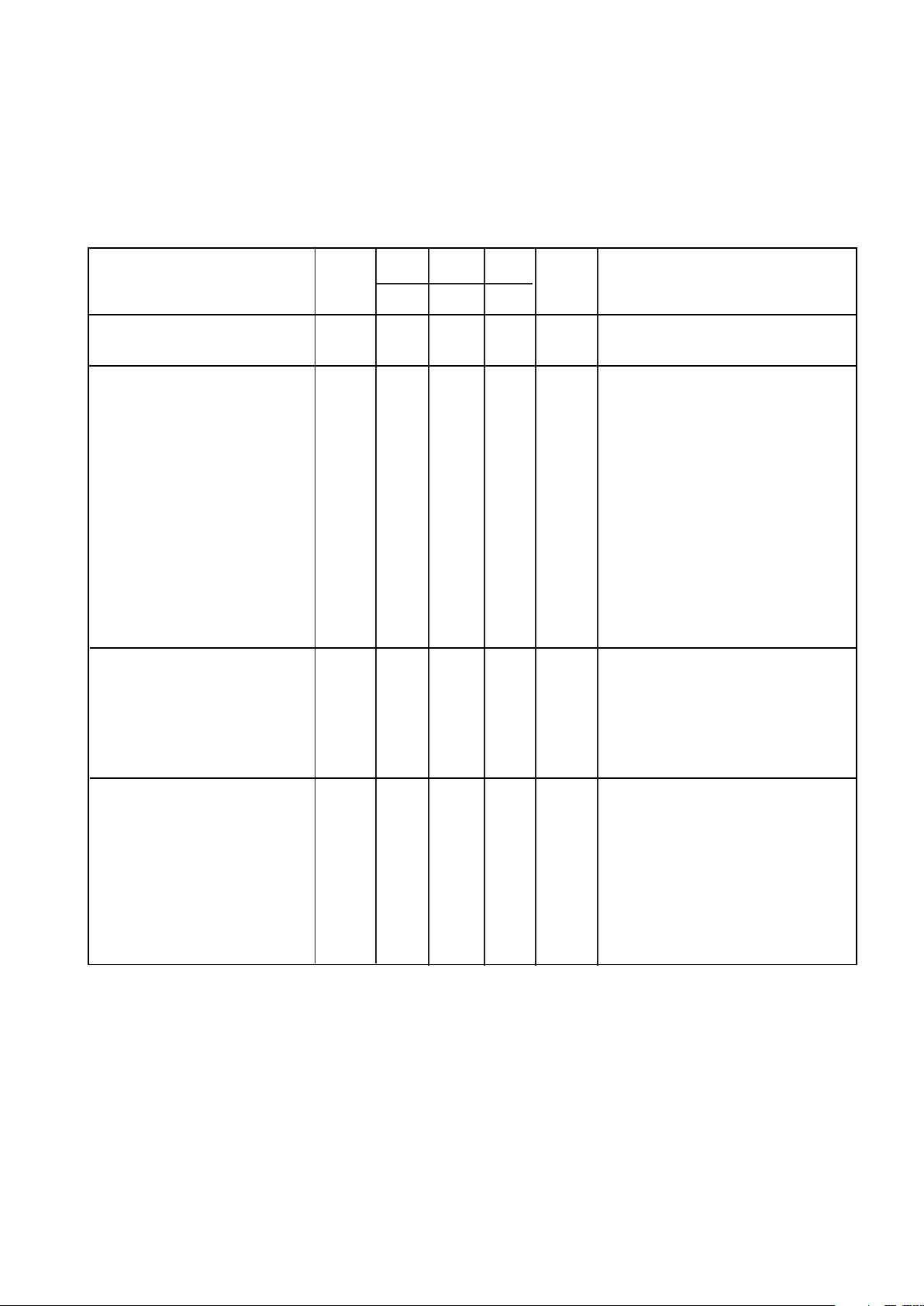
ELECTRICAL CHARACTERISTICS
These characteristics are guaranteed by either production test or design. They apply within the specified
ambient temperature and supply voltage unless otherwise stated.
T
AMB
= -20°C to + 80°C, VCC= + 4.75V to 5·25V.
IF = 403.25MHz or 479.5MHz; IF bandwidth up to 54MHz maximum. RF input frequency = 950MHz - 2150MHz.
Characteristic
Value
Min
Typ Max
Units
Conditions
Supply Current, I
CC
5,6,17 80 115 mA
RF input Noise figure at 3,4 16 dB @ T
amb
= 27°C
maximum gain
Variation of Noise Figure with 1 dB/dB
AGC setting
Conversion gain AGC bandwidth 100kHz
minimum AGC gain -15 -5 dB AGC = 4.0V
maximum AGC gain 25 33 dB AGC = 1.0V
AGC = self bias (2.4V)
Gain inband ripple -0.25 +0.25 dB Channel bandwidth 27MHz
Gain variation across RF input -2 +2 dB
range
Gain imbalance between IF 12,13 -2 +2 dB
outputs 18,19
RF input impedance, single 3,4 50 Ω @ T
amb
= 27°C
ended
RF input return loss 3,4 8 12 dB Input unmatched @ T
amb
= 27°C
RF input IP2 3,4 12 14 dBm See note 2
RF input IP3 3,4 -1 1 dBm See note 2
RF input IP3 variation with gain See Fig. 6
Input referred 1dB gain See Fig. 8
compression
Two tone IM2 distortions with -31 -33 dBc See note 2
Two tone IM3 distortions -36 -40 dBc See note 2
LO tuning range 7,8 1250 2700 MHz Maximum range of 1.4GHz within
band, application circuit as in Fig. 4.
LO phase noise 7,8 -75 dBc/Hz SSB at 10kHz offset, application
circuit as in Fig. 4. ƒ
LO
=2.63GHz
Pin
Page 14
14
SL2015
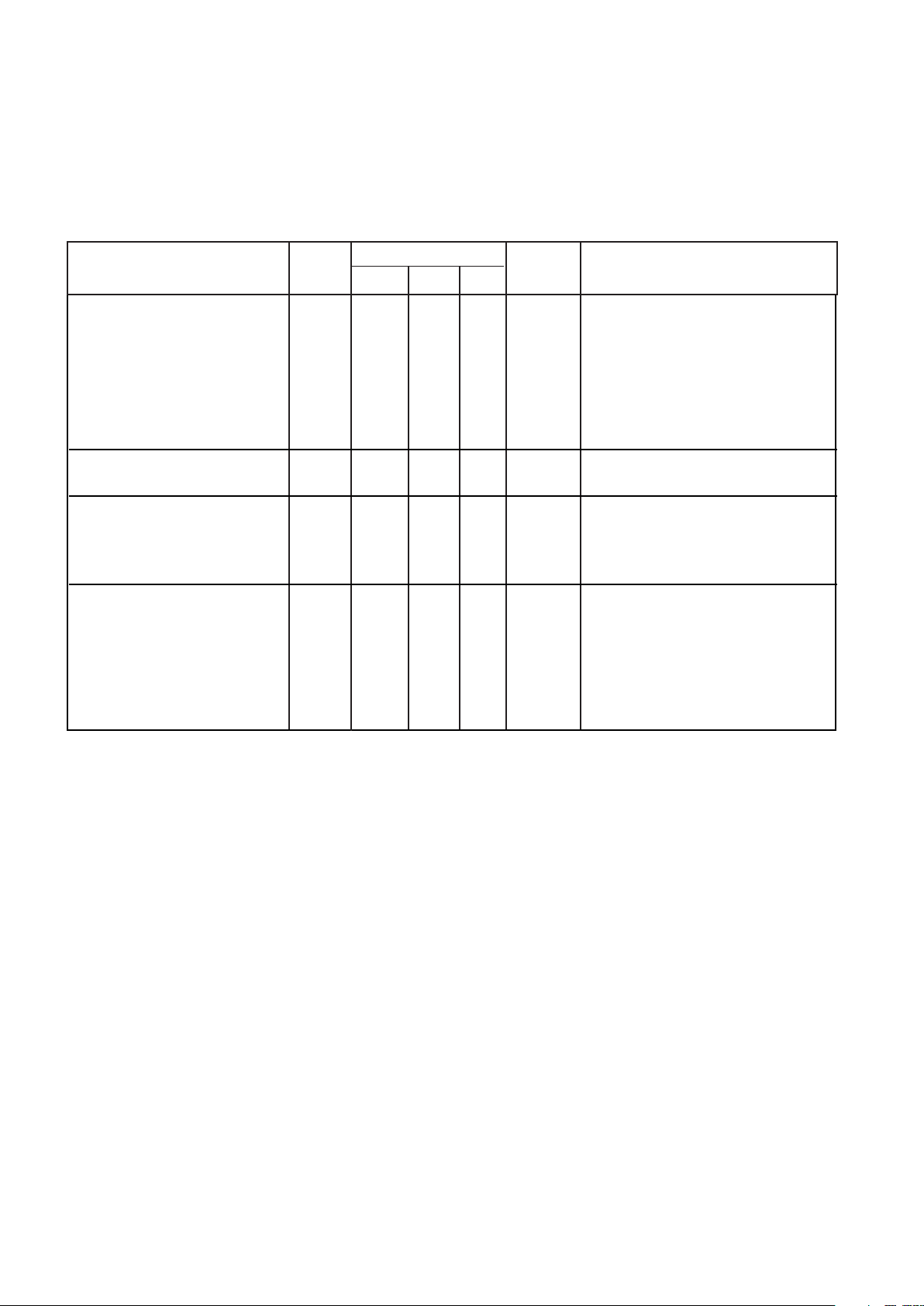
LO leakage to RF input 3,4,7,8 -30 dBm
LO leakage to IF outputs 7,8,12 -10 dBm Maximum conversion gain
LO output drive 15,16 92 dBµV Differential into 100Ω,
NB, synthesiser should be driven
differentially
LO output impedance 15,16 100 Ω Differential
LO output return loss 15,16 8 dB
AGC gain control slope variation 20 Monotonic from V
EE
to V
CC.
See Fig. 9
AGC control input current 20 -250 250 µA
Output select low voltage 10 0.7 V O/P 2 enabled, O/P 1 disabled
Output select high voltage 10 V
CC
-0.7 V O/P 1 enabled, O/P 2 disabled
Output select low current 10 -50 µA
Output select high current 10 200 µA
IF output 1 & 2 12,13, Output in enabled and disabled state
18,19
Output impedance 50 Ω Single ended
Return loss 12 dB
IF output 1 to 2 isolation 12,13 30 dB
18,19
Characteristic
Value
Min
Typ Max
Units
ConditionsPin
ELECTRICAL CHARACTERISTICS
These characteristics are guaranteed by either production test or design. They apply within the specified
ambient temperature and supply voltage unless otherwise stated.
T
AMB
= -20°C to + 80°C, VCC= + 4.75V to 5·25V.
IF = 403.25MHz or 479.5MHz; IF bandwidth up to 54MHz maximum. RF input frequency = 950MHz -2150MHz.
Notes:
1. All dBm units refer to a 50Ω system
2. Applies for any two carriers within band at -19dBm, and with AGC set for +5dB conversion gain.
Page 15
15
SL2015
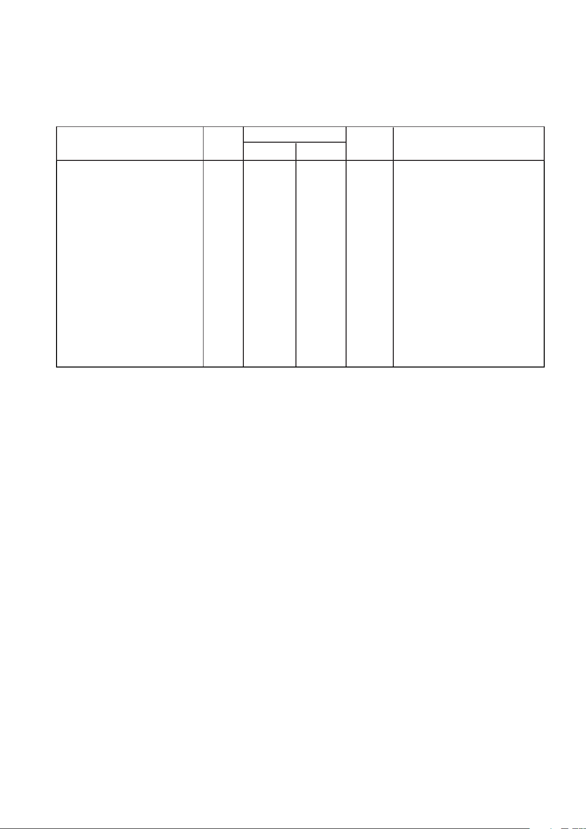
ABSOLUTE MAXIMUM RATINGS
All voltages are referred to VEE = 0V (pins 1,2,9,11,14)
Supply voltages V
CC
5,6,17 -0.3 7 V Transient
RF input voltage 3,4 2.5 Vp-p
RF input DC offset 3,4 -0.3 V
CC
+0.3 V
Tank inputs DC offset 7,8 -0.3 VCC+0.3 V
LO output drive DC offset 15, 16 -0,3 VCC+0.3 V
IF-OP-SEL input DC offset 10 -0.3 V
CC
+0.3
IF outputs 1 and 2 DC offset 12, 13 -0.3 VCC+0.3 V
18, 19
AGC Control input DC offset 20 -0.3 V
CC
+0.3 V
Storage temperature -55 +150 °C
Junction temperature +150 °C
QP20 thermal resistance 100 °C/W
Power consumption at V
CC
=5.25V 580 mW
ESD protection ALL 1.75 kV Mil std 883 latest revision
method 3015 class 1.
Parameter
Value
Min
Max
Units
Conditions
Pin
Page 16
Page 17

M Mitel (design) and ST-BUS are registered trademarks of MITEL Corporation
Mitel Semiconductor is an ISO 9001 Registered Company
Copyright 1999 MITEL Corporation
All Rights Reserved
Printed in CANADA
TECHNICAL DOCUMENTATION - NOT FOR RESALE
World Headquarters - Canada
Tel: +1 (613) 592 2122
Fax: +1 (613) 592 6909
North America Asia/Pacific Europe, Middle East,
Tel: +1 (770) 486 0194 Tel: +65 333 6193 and Africa (EMEA)
Fax: +1 (770) 631 8213 Fax: +65 333 6192 Tel: +44 (0) 1793 518528
Fax: +44 (0) 1793 518581
http://www.mitelsemi.com
Information relating to products and services furnished herein by Mitel Corporation or its subsidiaries (collectively “Mitel”) is believed to be reliable. However, Mitel assumes no
liability for errors that may appear in this publication, or for liability otherwise arising from the application or use of any such information, product or service or for any infringement of
patents or other intellectual property rights owned by third parties which may result from such application or use. Neither the supply of such information or purchase of product or
service conveys any license, either express or implied, under patents or other intellectual property rights owned by Mitel or licensed from third parties by Mitel, whatsoever.
Purchasers of products are also hereby notified that the use of product in certain ways or in combination with Mitel, or non-Mitel furnished goods or services may infringe patents or
other intellectual property rights owned by Mitel.
This publication is issued to provide information only and (unless agreed by Mitel in writing) may not be used, applied or reproduced for any purpose nor form part of any order or
contract nor to be regarded as a representation relating to the products or services concerned. The products, their specifications, services and other information appearing in this
publication are subject to change by Mitel without notice. No warranty or guarantee express or implied is made regarding the capability, performance or suitability of any product or
service. Information concerning possible methods of use is provided as a guide only and does not constitute any guarantee that such methods of use will be satisfactory in a specific
piece of equipment. It is the user’s responsibility to fully determine the performance and suitability of any equipment using such information and to ensure that any publication or
data used is up to date and has not been superseded. Manufacturing does not necessarily include testing of all functions or parameters. These products are not suitable for use in
any medical products whose failure to perform may result in significant injury or death to the user. All products and materials are sold and services provided subject to Mitel’s
conditions of sale which are available on request.
 Loading...