

Page 1
The SL1711 is a quadrature downconverter, intended
primarily for application in professional and consumer digital
satellite tuners.
The device contains all elements necessary, with the
exception of external local oscillator tank to form a complete
system operating at standard satellite receiver intermediate
frequencies. It is intended for use with external carrier
recovery.
The device includes a low noise RF input amplifier, a
reference VCO with prescaler output buffer and In-phase and
Quadrature mixers with baseband buffer amplifiers containing
AGC gain control.
The SL1711 is optimised to drive a dual ADC converter
such as the VP216.
The SL1711 utilises a power MP package, whereas the
SL1711B variant uses a standard MP16 plastic package and
features a revised operating temperature.
FEATURES
■ Single chip system for wideband quadrature
downconversion
■ Compatible with all standard high IF frequencies
■ Excellent gain and phase match up to 30MHz
baseband
■ High output referred linearity for low distortion and
multi channel application
■ Simple low component application
■ Fully balanced low radiation design with fully
integrated quadrature generation
■ High operating input sensitivity
■ On-board AGC facility
■ On chip oscillator for varactor tuning or SAW
resonator operation
■ ESD protection (Normal ESD handling procedures
should be observed)
MH16
SL1711
116
VCCC
AGC
IOUT
VEEA
IFINB
IFIN
IVCCA
QOUT
VEEC
VCCB
VCODIS
VCO B
VCO A
VEEB
PSCAL
PSCALB
APPLICATIONS
■ Satellite receiver systems
■ Data communications systems
■ Cable systems
ORDERING INFORMATION
SL1711/KG/MH1P (Sticks)
SL1711/KG/MH1Q (Tape and Reel)
SL1711B/KG/MP1S (Sticks)
SL1711B/KG/MP1T (Tape and Reel)
Fig. 1 Pin allocation
MP16
SL1711B
116
VCCC
AGC
IOUT
VEEA
IFINB
IFIN
IVCCA
QOUT
VEEC
VCCB
VCODIS
VCO B
VCO A
VEEB
PSCAL
PSCALB
SL1711
Quadrature Downconverter
Preliminary Information
Supersedes November 1996 version, DS4032 - 1.6 DS4032 - 4.0 October 1997
Page 2
2
SL1711
QUICK REFERENCE DATA
Characteristic Value Units
Input noise figure, DSB 17 dB
Maximum conversion gain 44 dB
Minimum conversion gain 28 dB
IP32T output referred +8 dBV
Output clip voltage 1.5 Vp-p
Gain match up to 22MHz ± 0.3 dB
Gain match up to 30MHz ± 0.5 dB
Phase match up to 30MHz ± 1.5 deg
Gain flatness up to 30MHz ± 0.5 dB
VCO phase noise, SSB @ 10kHz offset - 96 dBc/Hz
Prescaler division ratio 32
Prescaler output swing 1.6 Vp-p
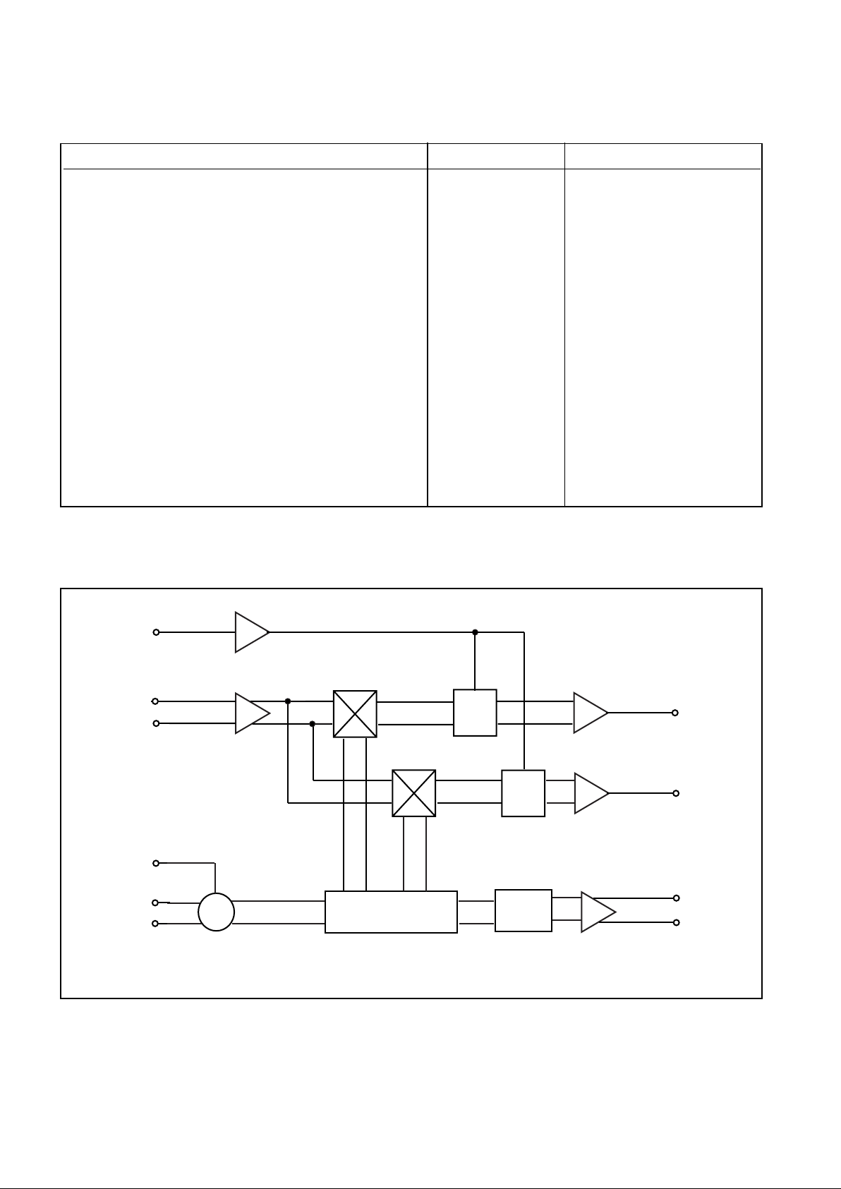
Fig. 2 SL1711 block diagram
AGC
IFIN
VCODIS
VCOA
AGC
AGC
÷32
LO
0 deg 90 deg
Quadrature
generator
PSCALB
PSCAL
Q OUT
I OUT
IFINB
VCOB
Page 3

3
SL1711
FUNCTIONAL DESCRIPTION
The SL1711 is a wideband quadrature downconverter,
optimised for application in both professional and consumer
digital satellite receiver systems and requiring a minimum
external component count. It contains all the elements
required for construction of a quadrature demodulator, with
the exception of tank circuit for the local oscillator.
A block diagram is shown in Fig. 2.
The SL1711 oscillator can be used with either a varator
tuned tank circuit or with a SAW resonator. Both
configurations are described in the Application Notes section
of this Data Sheet.
A typical digital satellite tuner application from tuner input
to data transport stream is shown in Fig. 13
In normal application the second satellite IF frequency of
typically 402.75 or 479.5 MHz is fed from the tuner SAW filter
to the RF preamplifier, which is optimised for impedance
match and signal handling. The amplifier output signal is then
split into two balanced channels to drive the In-phase and
Quadrature mixers. The typical RF input impedance is shown
in Fig. 3
In-phase and Quadrature LO signals for the mixers are
derived from the on board local oscillator, which uses an
external varactor tuned resonant network and is optimised for
low phase noise. The VCO also drives an on board divide by
32 prescaler whose outputs can be used for driving an external
PLL control loop for the VCO, where the PLL loop is contained
within the QPSK demodulator, for example the VP305. For
optimum performance in the varactor tuned application the
VCO should be fully symmetric. The VCO has a disable facility
by grounding pin 15, VCODIS; in normal applications this pin
is pulled to Vcc via a 4K7 resistor.
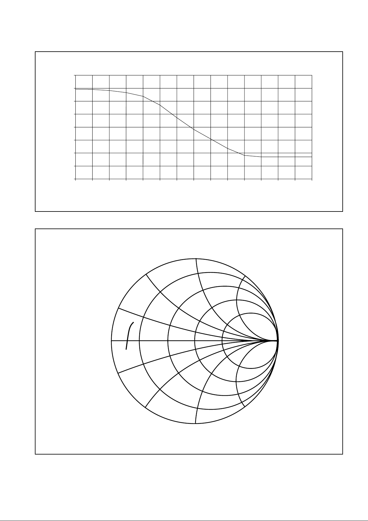
The mixer outputs are fed to balanced baseband AGC
amplifier stages, which provide for a minimum of 16 dB of AGC
control. The typical AGC characteristic is shown in Fig. 4.
These amplifiers then feed a low output impedance true
differential to single-ended converter output stage. In normal
application the output can be either directly AC coupled to the
ADC converter such as the VP216, which will generally have
a high input impedance, or to drive an anti alias filter. In this
later case the maximum load presented to the SL1711 must
not exceed a parallel combination of 1KΩ and 20pF. The
typical baseband output impedance is contained in Fig. 5.
It is recommended that the device is operated with an
output amplitude of 760mV under lock conditions.
Under transient conditions the output should not exceed
the clipping voltage.
Input and output interface circuitry is contained in Fig. 6.
The typical key performance figures at 480 MHz IF, 5V Vcc,
1 kΩ load and 25 deg C ambient are contained in table headed
'QUICK REFERENCE DATA'. With SAWR oscillator
application the gain and phase match performance will
typically exceed these numbers.
Page 4
4
SL1711
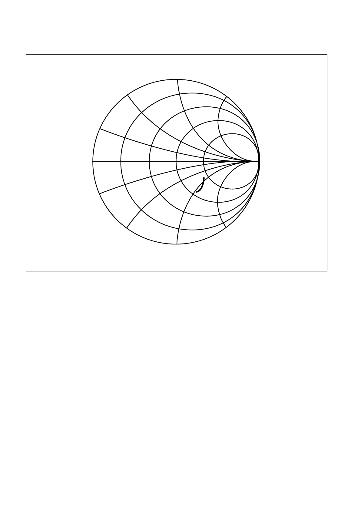
Fig.3 Typical RF input impedance
-j0.2
0
+j0.2
+j0.5
+j1
+j2
-j2
-j1
-j0.5
0.2 0.5
1
START 350 MHz
STOP 650 MHz
Marker 1 480MHz
Zreal = 96Ω
Zimag = 54Ω
X
Page 5
5
SL1711
Fig.4 Typical AGC characteristic
Fig. 5 Typical baseband output impedance
-j0.2
0
+j0.2
+j0.5
j1
+j2
-j2
-j1
-j0.5
0.2
0.5
1
X
X
1
2
1 1MHz
2 15MHz
3 30MHz
X
3
CONVERSION GAIN dB
15
20
25
30
35
40
45
50
55
1
1.25
1.5
1.75
2
2.25
2.5
2.75
3
3.25
3.5
3.75
4
4.25
4.5
AGC CONTROL VOLTS
Page 6
6
SL1711
IF Input
VCO
I & Q baseband output
VCO disable input
Prescaler outputs
AGC input
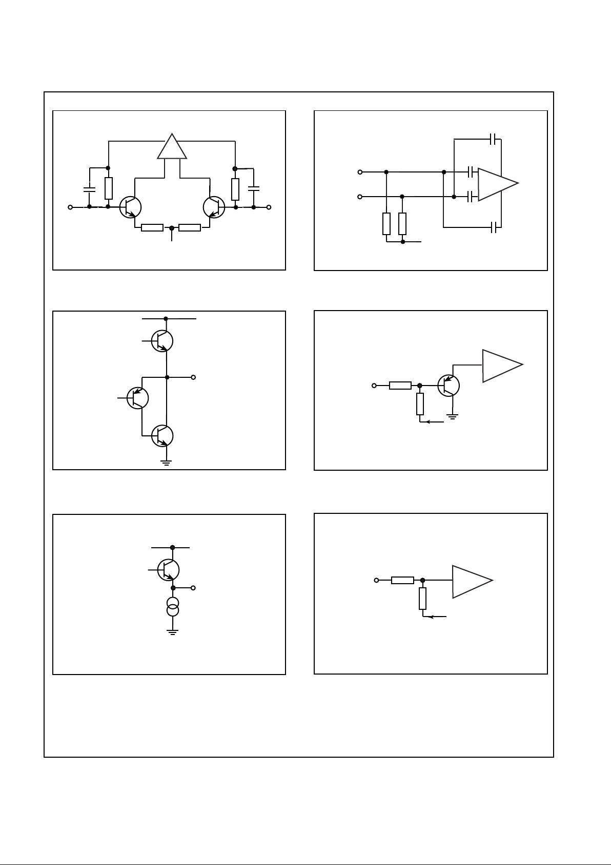
Fig. 6 I/O port peripheral circuitry
IFINB
IFIN
Vcc
O/P
O/P
Vcc
Vref
AGC
50k
Vref
VCO
VCO
2x20k
VCODIS
55k
Vref
Page 7

7
SL1711
CH PUMP
1
XTAL1
2
XTAL2
3
SDA
4
SCL
5
P7
6P67P58
P49P310NC11Vcc12RF I/P13RF I/P14Vee15DRV
16
IC2
SP5611
AGC
1
IOUT
2
VEEA
3
IFINB
4
IFIN
5
VCCA
6
QOUT
7
VEEC
8
VCCC
9
PSCALB
10
PSCAL
11
VEEB
12
VCOA
13
VCOB
14
VCODIS
15
VCCB
16
/32
Osc
I Mixer
Q Mixer
IC 1 SL1711
L1
12nH
C12
3p9
D1
BB811
C13
3p3
1
42
3
LK2
T2
BCW31
5V
R4
110R
SK4
Q CH O/P
C11
220nF
SW1
VCO DISABLE
R2
4K7
5V
SK1
RF IN
C1
100nF
C2
100nF
R1
75R
L5
4u7
L6
4u7
C3
100nF
C4
100pF
C5
100nF
C6
100pF
C7
100nF
C8
100pF
+
C9
47uF
5V
5V 5V 5V
VR1
1K
R5
680R
R6
4K7
R7
680R
T1
BCW31
1
42
3
LK1
R3
110R
SK3
I CH O/P
C10
220nF
C14
10nF
C15
10nF
C19
220nF
C20
47nF
R8
22K
R9 22K
R10
4K7
T3
BCW31
R11
10K
C21
10nF
30V
C18
18pF
X1
4 MHz
C16
10nF
C17
100pF
1
2
3
CN1
DC POWER
30V
5V
SDA5
3
5V04GND5SCL5
6
SK4
I2C
5V
Fig.7 SL1711 standard evaluation board
Page 8

8
SL1711
Fig.8
Fig.9
Page 9

9
SL1711
AGC
1
IOUT
2
VEEA
3
IFINB
4
IFIN
5
VCCA
6
QOUT
7
VEEC
8
VCCC
9
PSCALB
10
PSCAL
11
VEEB
12
VCOA
13
VCOB
14
VCODIS
15
VCCB
16
/32
Osc
I Mixer
Q Mixer
IC1
SL1711
C1
100nF
C2
100nF
R1
75R
C3
100pF
C4
100nF
C5
100pF
C6
100nF
C7
100pF
C8
100nF
SW1
VCO DISABLE
R2
4K7
5V
5V
T1
BCW31
R3
110R
C10
220nF
T2
BCW31
R4
110R
C11
220nF
5V
SK2
I CH OUT
SK3
Q CH OUT
SK1
IF IN
+
C9
47uF
R6
4K7
VR1
1K
R5
680R
R7
680R
1
42
3
LK2
1
4
2
3
LK1
C13
1nF
TP1
AGC VOLTS
1
2
3
CN1
POWER
5V
SAW
RESONATOR
1
2 3
4
SAW1
C12
1nF
C14
100pF
C15
100pF
5V
5V
5V
Fig.10. SL1711 I & Q downconverter with SAW resonator
Page 10

10
SL1711
Fig. 11
Fig. 12
Page 11

11
SL1711
APPLICATION NOTES
These application notes should be read in conjunction with
circuit diagrams contained in Fig. 7 and 10, and a
recommended front end tuner solution contained in Fig. 13.
These boards have been designed to demonstrate
performance and to allow for initial evaluation of the SL1711.
Varator Tuned Oscillator
Refer to Fig. 7 circuit diagram and Figs. 11 and 12 PCB
layout.
This application uses a synthesised VCO with a tuning
range of 460 MHz to 500 MHz. The surface mount inductor L1
is 12 nH. The VCO frequency is controlled by the SP5611
synthesiser which is programmed via an I2C bus. The RF input
to the synthesiser is from the SL1711 prescaler outputs
coupled via RF inductors L3 and L4.
For functional checking the VCO can be tuned by
physically shorting the base of transistor T3 to ground and
then adjusting the +30 volt supply to tune the VCO. Under
these conditions, due to the unlocked state of the LO, the
board WILL NOT BE representative of locked gain and phase
match or phase noise performance.
In real applications such the VCO control voltage will be
provided by the QPSK demodulator circuit, such as the
VP305. This circuit provides a line voltage to align the
reference LO in the 1711 in both frequency and phase to the
centre of the modulation bandwidth, normally 402.75 or 479.5
MHz.
As in all feedback loops the bandwidth of the varactor line
must be optimised for the symbol rate of the received
modulation.
It is recommended for optimum performance that the VCO
application is implemented symmetrically, in presented drive
and impedance to the VCO ports, as demonstrated in the
evaluation schematic and PCB.
In the recommended application the varactor diodes are
referenced to the VCO port DC bias voltages. This limits the
minimum tuning voltage on the varactor line to 3V. If lower
tuning voltage is required the tank can be AC coupled to the
VCO ports by 390pF capacitor and a DC reference voltage for
the varactor diodes applied by centre tapping the tank
inductors. NB the varactor diodes require a minimum of 1V
reverse bias for correct operation.
In real applications the maximum tuning range required for
the VCO will be determined by the required lock range of the
tuner and the manufacturing tolerance of the tank, assuming
the quadrature downconverter section will be alignment free.
This tuning range will be typically be much smaller than the
demonstration board, which will consequently improve the
VCO phase noise performance.
This application can be ported direct to real system
implementations. Normal good RF practice must be applied to
the layout implementation.
Prescaler Outputs (varactor tuned VCO)
The VCO frequency divided by 32 is available at the
differential prescaler outputs, pins 10 and 11.
These enable the VCO frequency to be synthesised by a PLL
frequency synthesiser; on the demo board an SP5611 is used
for this function however in a real application this function will
be provided by the QPSK demodulator function contained in
for example the VP305
It is recommended that the prescaler outputs are loaded
symmetrically to balance radiation effects.
Saw Resonator Oscillator
Refer to Fig. 10 circuit diagram and Figs 11 and 12 PCB
layout.
In the standard application the oscillator uses a varactor
diode tuned tank circuit which allows fine tuning of the
oscillator frequency via a voltage control line. This control
voltage is usually derived from the QPSK/FEC decoder
VP305/VP306
Certain applications do not require this fine tune facility so
a fixed frequency application using a SAW resonator has been
developed. In this application the frequency of the oscillator is
determined by the SAW resonator. The SAW is AC coupled
into the VCO pins of the device pins 13 and 14 via 100pF
coupling capacitors.
The SAW resonator used in this application is a ;
Murata Part No SAR479.45MB10X200
Prescaler Outputs (SAWR tuned VCO)
The VCO frequency divided by 32 is available at the
differential prescaler outputs, pins 10 and 11. Normally these
outputs will not be required since the derotation and fine tuning
required will be processed by the QPSK demodulator.
However these frequencies could be used if required for other
system reference frequencies or clocks.
If used it is recommended that the prescaler outputs are
loaded symmetrically to balance radiation effects.
VCO Disable
The on-chip oscillator can be disabled by connecting
VCODIS, pin 15, to ground and enabled by connecting to Vcc
via a 4k7 Ω pull up resistor.
AGC
The AGC facility can be used to control the conversion gain
of the SL1711.
On the demonstration boards the conversion gain is
adjusted by means of a potentiometer, which is set to 2.5V so
giving a conversion gain of 38 dB. The voltage adjustment
range for the AGC is approximately 1.5 to 3.5 V.
It is important that the AGC voltage minimum does not give
a conversion gain of greater than 44dBs otherwise the
channel amplitude match may be degraded. In real
applications the AGC can be either set at a fixed control
voltage or controlled by means of the AGC control signal from
the QPSK demodulator dependant on the overall dynamic
range requirement of the tuner and it’s gain distribution.
Page 12

12
SL1711
I & Q baseband outputs
The SL1711 offers a greatly improved drive capability over
the SL1710 and as such is much less sensitive to the load
conditions.
It is still important however to carefully balance the loads
presented to the SL1711 to ensure no differential gain or
phase degradation is introduced by the load circuits, which will
also include effects due to track striplines etc.
For demonstration purposes the output is unsuitable for
connection via co-axial cables to standard test equipment,
where such equipment is normally 50 Ω or highly capacitive.
To overcome this problem the outputs of the SL1711 are
therefore buffered through emitter followers which are
optimised to drive 50 Ω loads without appreciable degradation
in the SL1711 performance. These buffer stages are
selectable so enabling the outputs to be loaded directly for
interfacing direct with an ADC via a low capacitive link.
In most applications the SL1711 will normally interface
direct into the ADC converter such as the VP216, which will
present a >1 kΩ low capacitive load, though it can interface
with lower impedances if desired.
The output is optimised for typical drive levels of 760
mVp-p and the onset of clipping is typically > 1.5V.
Care must be taken with system design to ensure that the
I and Q baseband output signals never exceed 1.2V pk-pk.
Any gross distortion in the output waveform caused by
overdriving the output stages will compromise the system
performance.
Device performance characteristics can only be
guaranteed if the device is operated below the onset of
clipping.
SL1711 Evaluation Board
This board has been created to show the operation of the
SL1711 I/Q downconverter.
It does not attempt to simulate a real system, since in
practice the 479.5MHz IF oscillator on the SL1711and the
60MHz clock on the subsequent ADC would be controlled via
the baseband IQ demodulator chip such as the VP305 which
follows the dual channel ADC. For simplicity, the VCO is
locked using Mitel Semiconductor SP5611 synthesiser, controlled via an I2C bus.
For full evaluation, 30V and 5V supplies are necessary.
Supplies
The board must be provided with the following supplies:
A) 5V for the SL1711 and SP5611 and 30V for the
varactor line.
The supply connector is a 3 pin 0.1" pitch pin header. The
centre pin of the connector is GND.
Outputs driven into hard clipping can exhibit amplitude
decline. AGC loops should be designed to take account of this.
I2C Bus connections
The board is provided with an RJ11 I2C bus connector
which feeds directly to the SP5611 synthesiser.
This connects to a standard 6-way connector cable which
is supplied with the I
2
C/3-wire bus interface box.
Input and Output connections
The board is provided with the following connectors:
A) IF I/P SMA connector SK1 which is AC coupled to the
RF input of the SL1711.
B) I CH OUT SK2 and Q CH OUT (SK3) which provide
either a buffered or direct baseband output signal from
the SL1711 (depending on which way the links LK1
and LK2 are set). The output buffers should be used
when driving 50Ω test equipment or co-axial lines.
Links and Switches
The board is provided with the following:
VCO DISABLE switch
This disables the VCO of the SL1711. It does NOT power
down the chip.
AGC ADJUST potentiometer
The potentiometer sets the AGC input voltage of the
SL1711 which controls the gain of the chip. TP1 is provided as
a means of monitoring the AGC voltage.
LK1 and LK2
These are links which may be placed either vertically or
horizontally to connect the outputs of the SL1711 either
directly or via buffers to the SMA output connectors of the
board.
If the links are placed vertically 1-2 and 3- the outputs are
connected directly.
If the links are placed horizontally 1-3 and 2- the ouputs are
connected via buffers.
Page 13

13
SL1711
Programming of Synthesisers
A SP5611 synthesiser is used to set the frequency of the
SL1711 VCO 480MHz. Since the SL1711 incorporates a
divide by 32 the synthesised frequency that the SP5611 must
be programmed to is 480/32=15MHz.
Example
a) To program the SL1711 to 480MHz.
I2C Byte Hex Code
Byte 1 (address) C2
Byte 2 (programmable divider 8 MSBs) 00
Byte 3 (programmable divider 8 LSBs) F0
Byte 4 (control data) CE
Byte 5 (port data) 00
C2 is the address byte byte 1.
0F00 is the programmable divider information bytes 2 and 3.
CE is the control data information byte 4.
**Note - the programmable divider information should be
set to program 480MHz /32 = 15MHz since the SL1711
provides a divide by 32 prescaler output rather than the VCO
carrier frequency.
It is not possible to program the VCO to 479.5MHz when
using a 7.8125kHz phase comparator frequency. The minimum step size is 7.8125kHz x 8 (RF prescaler inside SP5611)
x 32 (SL1711 output prescaler) = 2MHz.
If the reference divider is set to 1024 mode3.90625kHz
phase comparator frequency, the minimum step size will be
1MHz.
This may be achieved by programming the control byte to
CC and modifying the programmable divider information for
the new step size.
SL1711 Operation
The SL1711 will mix an IF input with its own local oscillator.
This is controlled as above via a SP5611 synthesiser.
Normally the VCO will be set to the same frequency as the
IF input, and the signal mixed directly down to baseband.
Alternatively, a CW RF source may be fed into the input of
the SL1711 which is deliberately offset from the VCO. By
varying the offset from 0-20MHz and monitoring the I and Q
channel baseband outputs, the flatness response of the chip/
output filter can be measured.
The SL1711 oscillator may also be disabled by setting the
ON-VCO-OFF switch to the OFF position.
An AGC voltage adjust pot marked AGC ADJUST is
provided, together with a test point.
Measurement of Gain and Phase Match.
a)Synthesise the required frequency 480MHz is used in the
example above.
b)Connect an RF signal generator to the input.
c)Input a signal which should give an output of approx 0dBm
(0.707V p-p), in combination with the appropriate AGC setting.
d) Connect a vector voltmeter to the BUFFERED outputs
when using 50Ω inputs. When using high impedance probes,
the direct outputs may be used. Selection of outputs is via the
on board U links.
e)CALIBRATE the vector voltmeter and the leads to be used.
The calibration should be performed at the chosen baseband
frequency and level for maximum accuracy.
f) Vary the RF input frequency either side of the LO and note
the relative I and Q gain and phase reading.
If you experience any difficulties with this board, or require
further help, please contact
Robert Marsh
on 01793 518234
or
Fred Herman
on 01793 518423
Page 14

14
SL1711
Fig.13 Example digital front end architecture
Note: All ICs shown in Fig. 13 are available from Mitel Semiconductor.
AGC
RF I/P
from
LNB
I/P
Filter
950MHz
2.15GHz
TUNER
(SL2015)
Tank
circuit
480MHz IF
IF
Filter
RF TUNER
MODULE
AGC
TANK
AGC
VCO
I
Q
PLL SYNTH. options
(SP5658) (3w bus)
(SP5055) (I2C bus)
(SP5655) (I2C bus)
(SP5659) (I2C bus)
0.22MHz
0.7V pk-pk
(SL1711)
2x6 bit, 90MS/s
ADC
(VP216)
VCO I/p
Loop/line
Filters
QPSK
Demod & FEC
(VP305)
Data
Stream
Page 15

15
SL1711
ELECTRICAL CHARACTERISTICS
Test conditions (unless otherwise stated)
T
amb
= 0oC to 85oC,
* V
ee
= 0V, Vcc = 4.75 to 5.25 V, Fif = 479.5 MHz, IF bandwidth ± 22 MHz, output amplitude -11dBV
These characteristics are guaranteed by either production test or design. They apply within the specified ambient temperature
and supply voltage unless otherwise stated.
Characteristic Pin Min Typ Max Units Conditions
Supply voltage 6,9,16 4.75 5.25 V
Supply current 6,9,16 109 125 mA
IF input operating 4, 5 350 550 MHz
frequency (1)
IF input impedance 4, 5 75 Ω Over specified frequency
operating range, see Fig. 6.
Input return loss 4, 5 12 dB Over specified frequency
operating range, see Fig. 6.
Input noise figure, DSB 4, 5 17 19 dB Maximum gain setting
Variation in NF with gain 1 dB/dB
setting
VCO operation range 350 550 MHz Centre frequency and tuning
range determined by
application.
VCO phase noise, SSB 96 -85 dBc/Hz Varactor tuned, determined
@ 10kHz offset by application.
VCO Vcc sensitivity 2E3 ppm/V Free running
VCO temperature 100 ppm/°C Uncompensated
stability
Prescaler output swing 10, 11 1.2 1.6 Vp-p
Prescaler output duty 10, 11 40 50 60 %
cycle
Conversion gain for See Fig. 4
AGC setting of;
1.5V 44 dB Terminated voltage
conversion gain from 50Ω
source to 1kΩ load
2.5V 38 dB
3.5V 28 dB
AGC input current 1 100 µA All AGC settings
I Q gain match ±0.3 ±1 dB See Note 3.
I Q gain match ±0.5 ±1 dB See Note 4.
I Q phase match ±1.5 ±3 deg See Note 4.
I & Q channel in band ripple ±0.3 ±1 dB see Note 3.
I & Q channel in band ripple ±0.5 ±1 dB See Note 4.
I Q crosstalk -29 -20 dB See Note 4 and Note 2 for
derivation of cross modulation
Page 16

16
SL1711
ELECTRICAL CHARACTERISTICS (continued)
Test conditions (unless otherwise stated)
T
amb
= 0oC to 85oC,
* V
ee
= 0V, Vcc = 4.75 to 5.25 V, Fif = 479.5 MHz, IF bandwidth +- 22 MHz
These characteristics are guaranteed by either production test or design. They apply within the specified ambient temperature
and supply voltage unless otherwise stated.
Characteristic Pin Min Typ Max Units Conditions
I & Q baseband output 2,7 8 20 Ω See note (5), and Fig. 5.
impedance
I & Q baseband output 2, 7 1.2 1.5 Vp-p See note(6), into 1KΩ load up to
clipping level 22MHz baseband
IP3
2T
, output referred +3 +9 dBV 2 input carriers at -39 dBV
within IF bandwidth of ±22MHz
AGC set to give composite
output of -11 dBV, IM3 tone
within baseband bandwidth
IM3
2T
output referred -40 dBc 2 input carriers within IF
bandwidth of ±22MHz, AGC
set to give composite output
of -11 dBV, IM3 tone within
baseband bandwidth
All prescaler and other -30 dBc 0.1 - 100MHz, referred to output
spurs in I & Q baseband amplitude of - 11 dBV.
output.
Power supply rejection 20 dBc Attenuation Vcc to I & Q outputs,
over 0-500kHz
Notes: 1. Performance not guaranteed over full specified IF input operating range
2. I Q crosstalk is determined from the gain and phase match by the following formula
Crosstalk = 20* Log (tan(phase error + Atan (1+amplitude imbalance) -45°))
3. Over specified gain dynamic, 1kΩ load up to 22MHz baseband
4. Over specified gain dynamic range, 1kΩ load up to 30MHz baseband
5. Baseband bandwidth 0.1 to 22MHz
6. The device should not be operated beyond the point of output clipping. The quality and amplitude of the
baseband output signals cannot be guaranteed once this level has been exceeded.
7.
* Operating temperature range for the SL1711B is 0°C to 70°C. This applies to applications featuring a double
sided copper board. For other applications not using such a board, the maximum operating
temperature may be reduced.
8. The above device characteristics are guaranteed provided the output is maintained below the onset of clipping.
Page 17

17
SL1711
ABSOLUTE MAXIMUM RATINGS
All voltages are reffered to Vee at 0V
Characteristics Min Max Units Conditions
Supply voltage, Vcc -0.3 7 V
IFFIN &IFINB input voltage 2.5 Vp-p
IFIN & IFINB input DC offset -0.3 Vcc+0.3 V
IOUT & QOUT DC offset -0.3 Vcc+0.3 V
AGC DC offset -0.3 Vcc+0.3 V
VCO1 & 2 DC offset -0.3 Vcc+0.3 V
VCODDIS DC offset -0.3 Vcc+0.3 V
PSCAL & PSCALB DC offset -0.3 Vcc+0.3
Storage temperature -55 125 °C
Junction temperature 150 °C
PSOP16 package thermal TBA °C/W
resistance, chip to ambient
PSOP16 package thermal TBA °C/W
resitance, chip to case
MP16 package thermal resistance 81 °C/W
chip to Ambient
MP16 package thermal resistance 28 °C/W
chip to case
Power consumption at 5.25V 657 mW
ESD protection 2 kV Mil std 883B method 3015 cat 1
ADDITIONAL INFORMATION REGARDING THE PSOP PACKAGE.
The following information should be noted when using the PSOP package fitted to the SL1711.
(a) This package uses the standard SOIC 16 footprint.
(b) There is no need to make a thermal connection between the package and the board. If such a connection is made using
a thermal adhesive this will enhance the long term reliability of the product by reducing the junction temperature.
(c) The heatsink that is evident on the base of the package is solderable.
(d) There is no direct electrical connection between any of the device pins and the metal heatsinkslug. However if the
heatsink is to be electrically connected to the PCB these connections should be confined to the ground plane.
Page 18

Page 19

Page 20

M Mitel (design) and ST-BUS are registered trademarks of MITEL Corporation
Mitel Semiconductor is an ISO 9001 Registered Company
Copyright 1999 MITEL Corporation
All Rights Reserved
Printed in CANADA
TECHNICAL DOCUMENTATION - NOT FOR RESALE
World Headquarters - Canada
Tel: +1 (613) 592 2122
Fax: +1 (613) 592 6909
North America Asia/Pacific Europe, Middle East,
Tel: +1 (770) 486 0194 Tel: +65 333 6193 and Africa (EMEA)
Fax: +1 (770) 631 8213 Fax: +65 333 6192 Tel: +44 (0) 1793 518528
Fax: +44 (0) 1793 518581
http://www.mitelsemi.com
Information relating to products and services furnished herein by Mitel Corporation or its subsidiaries (collectively “Mitel”) is believed to be reliable. However, Mitel assumes no
liability for errors that may appear in this publication, or for liability otherwise arising from the application or use of any such information, product or service or for any infringement of
patents or other intellectual property rights owned by third parties which may result from such application or use. Neither the supply of such information or purchase of product or
service conveys any license, either express or implied, under patents or other intellectual property rights owned by Mitel or licensed from third parties by Mitel, whatsoever.
Purchasers of products are also hereby notified that the use of product in certain ways or in combination with Mitel, or non-Mitel furnished goods or services may infringe patents or
other intellectual property rights owned by Mitel.
This publication is issued to provide information only and (unless agreed by Mitel in writing) may not be used, applied or reproduced for any purpose nor form part of any order or
contract nor to be regarded as a representation relating to the products or services concerned. The products, their specifications, services and other information appearing in this
publication are subject to change by Mitel without notice. No warranty or guarantee express or implied is made regarding the capability, performance or suitability of any product or
service. Information concerning possible methods of use is provided as a guide only and does not constitute any guarantee that such methods of use will be satisfactory in a specific
piece of equipment. It is the user’s responsibility to fully determine the performance and suitability of any equipment using such information and to ensure that any publication or
data used is up to date and has not been superseded. Manufacturing does not necessarily include testing of all functions or parameters. These products are not suitable for use in
any medical products whose failure to perform may result in significant injury or death to the user. All products and materials are sold and services provided subject to Mitel’s
conditions of sale which are available on request.
 Loading...