

Page 1

L
0
1
2
3
4
5
6
7
8
Q
Q
0
SK19XX Family
1:9 Signal Distribution
HIGH-PERFORMANCE PRODUCTS
SK19XX Family Functional Block Diagram
PRELIMINARY
T
T0*
T
T1*
T
T2*
IN
LK
LK*
EL*
E
T
T3*
*
*
*
T
T4*
T
T5*
T
T6*
T
T7*
T
T8*
Revision 1/January 23, 2001
1
www.semtech.com
Page 2
SK19XX Family
1:9 Signal Distribution
HIGH-PERFORMANCE PRODUCTS
SK19XX Family Product Selection Guide
1:9 Signal Distribution
rewoP
ylppuS
tcudorP V3.3 V2.5
0091KS
1091KS
2091KS
3091KS
l l l
l l l
l l l
l l
nepO
rettimE
05 ΩΩΩΩΩ
Logic Family
elbuoD
noitanimreT
PRELIMINARY
3 GHz Synch / Asynch Operation
noitarugifnoCtuptuO tuptuO ytilibaliavA
lanretnI
05 ΩΩΩΩΩ ecruoS
noitanimreT
kniStnerruC
elbuoD(
)noitanimreT
LCEP/LCE woN
LTT/gniwSelbuoD woN
LCEP/LCE woN
LCEP/LCE woN
4091KS
l l l
tcudorP
5291KS LCEPotgnihtynA
6291KS LCEotgnihtynA
7291KS LCEPotgnihtynA
8291KS LCEotgnihtynA
9291KS LCEPotgnihtynA
0391KS LCEotgnihtynA
LCEP/LCE woN
Logic / Translation Family
noitalsnarT noitarugifnoCtuptuO ytilibaliavA
nepO
l
l
05 ΩΩΩΩΩ elbuoD
rettimE
noitanimreT
l
l
05 ΩΩΩΩΩ
ecruoS
noitanimreT
l
l
Open Collector Logic Family
noitarugifnoCtuptuO tnerruCtuptuO ytilibaliavA
woN
woN
woN
woN
woN
woN
tcudorProtcelloCnepO
9991KS
Revision 1/January 3, 2001
l
Am2110022Q
2
www.semtech.com
Page 3
SK19XX Family
1:9 Signal Distribution
HIGH-PERFORMANCE PRODUCTS
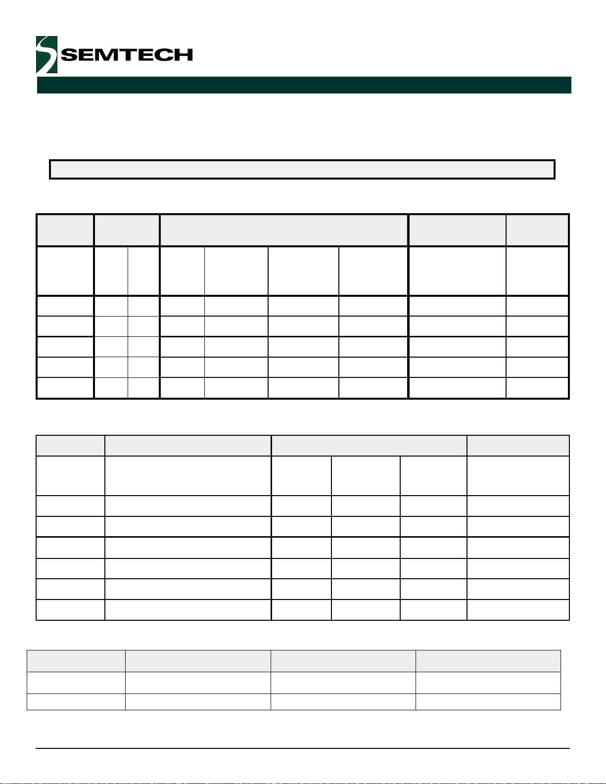
SK19XX Family Package Information
See
Figure 3.
5mm x 5mm TQFP
D, E
D1, E1
3
4
2
PRELIMINARY
b
8
Top View
e
A
A2
A1
10
b
Side View
SEATING
PLANE
Revision 1/January 3, 2001
3 www.semtech.com
Page 4

SK19XX Family
1:9 Signal Distribution
HIGH-PERFORMANCE PRODUCTS
HIGH-PERFORMANCE PRODUCTS
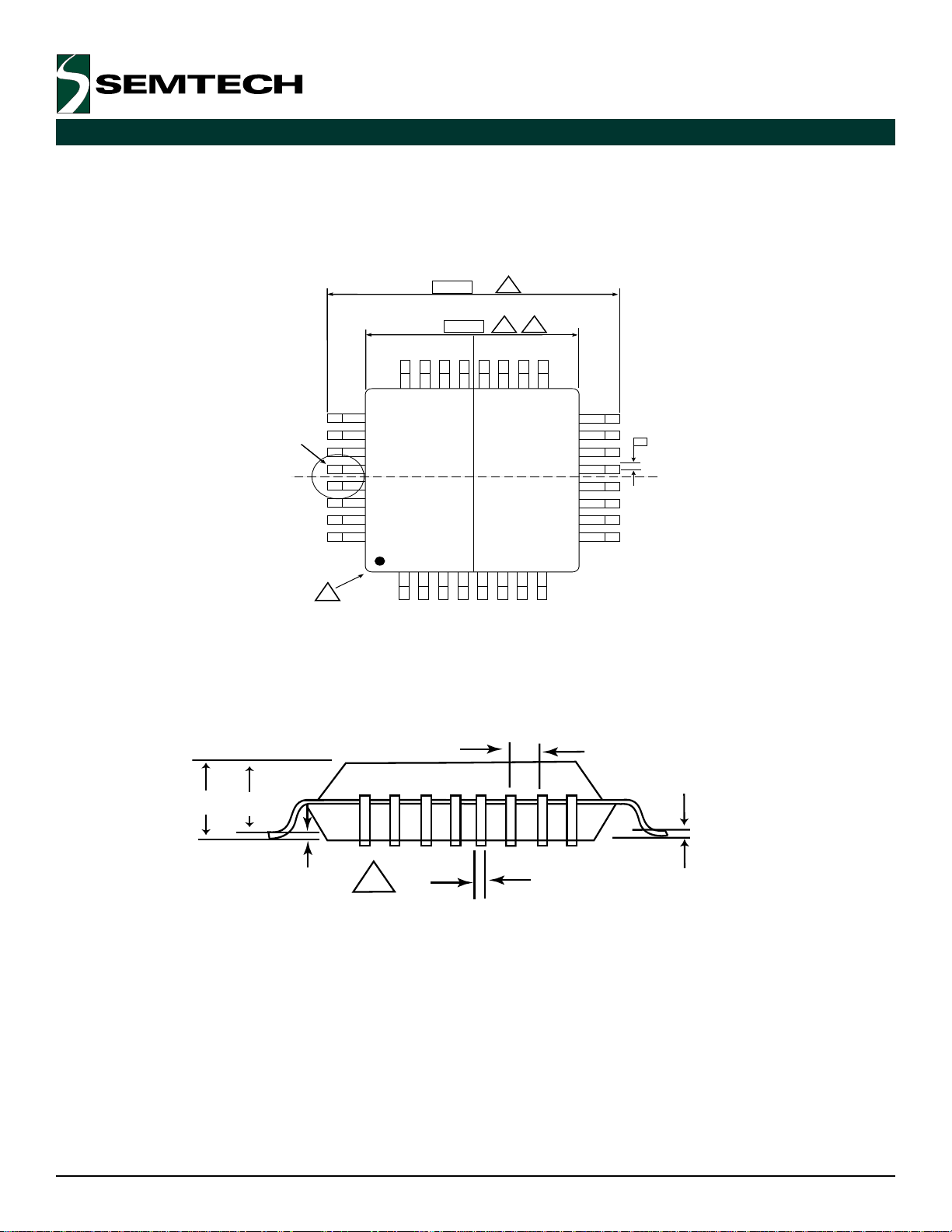
SK19XX Family Package Information (continued)
02
2
S
03
(L1)
Figure 1.
R1
01
R2
11
L
GAGE PLANE
25
00
5mm x 5mm TQFP
9
7
b
9
c
9
b1
Figure 2. Figure 3.
PRELIMINARY
WITH
PLATING
9
c1
e / 2
b
1. All dimensions and tolerancing conforms
to ANSI Y14.5M-1982.
2. The top package body size may be smaller
than the bottom package body size by as
much as 0.15 mm.
3. To be determined at seating plane.
4. Dimensions D1 and E1 do not include
mold protrusion. Allowable protrusion
is 0.25 mm per side. D1 and E1 are
maximum plastic body size dimensions
including mold mismatch.
5. Details of Pin 1 identifier optional, but
must be located within the zone indicated.
6. All dimensions are in millimeters.
7. Dimension b does not include Dambar
protrusion. Allowable Dambar protrusion
shall not cause the lead width to exceed
the maximum b dimension by more than
0.08 mm. Dambar cannot be located
on the lower radius or the foot. Minimum
space between protrusion and an
adjacent lead is 0.07 mm for 0.4 mm and
0.5 mm pitch packages.
8. Exact shape of each corner is optional.
9. These dimensions apply to the flat
section of the lead between 0.10 mm
and 0.25 mm from the lead tip.
10. A1 is defined as the distance from the
seating plane to the lowest point of the
package body.
Revision 1/January 23, 2001
JEDEC Variation
All Dimensions in Millimeters
lobmySNIMMONXAMetoNstnemmoC
A00.101.102.1thgieHffOdnatSegakcaP
1A50.001.051.0paGriA
2A59.000.150.1ssenkcihTydoBegakcaP
DCSB00.73
1DCSB00.52,4htgneLydoBegakcaP
ECSB00.73
1ECSB00.52,4htdiWydoBegakcaP
N23tnuoCdaeL
eCSB05.0hctiPdaeL
b71.022.072.07 ssenkcihTdaeL
1b71.002.032.0
1R80.0
2R80.002.0
o
000
100o
2011
3011
S02.0
c90.002.0
1c90.061.0
L54.006.057.0
1LFER00.1
ccc80.0
o
o
aaa02.0
bbb02.0
ddd80.0
4
o
5.3
o
21
o
21
o
7
o
31
o
31
www.semtech.com
Page 5

SK19XX Family
1:9 Signal Distribution
HIGH-PERFORMANCE PRODUCTS
Absolute Maximum Ratings*
Absolute Maximum Ratings*
lobmySretemaraP eulaVtinU
V
EE
V
CC
V
I
V
I
V(ylppuSrewoP
V(ylppuSrewoP
V(egatloVtupnI
V(egatloVtupnI
E
tnerruCtuptuO
I
TUO
suounitnoC
egruS
T
A
)V0=-0ot0.6V
CC
)V0=0ot0.6V
EE
CC
V,V0=
V,V0=
Vnahtevitageneromton
I
I
)0ot0.6-V
EE
Vnahtevitisoperomton
)0ot0.6V
CC
egnaRerutarepmeTgnitarepO 07+ot0
PRELIMINARY
05
001
Am
Am
o
C
T
gts
T
los
* Maximum Ratings are those values beyond which damage to the device may occur.
erutarepmeTegarotS 051+ot56-
o
542:sdnoces3ot2<(erutarepmeTredloS
C)derised562
o
C
o
C
Revision 1/January 23, 2001
5
www.semtech.com
Page 6

SK1900
CLKC
S
SEL
OUT0
OUT0
OUT1
OU
OUT2
OU
OUT3
OUT3
OUT4
OU
OUT5
OUT5
OUT6
OUT6
OUT7
OU
OUT8
OUT8
Q
Q
0
VCC
VEE
1.3V
3.3V
or
5.2V
700 mV
1:9 Signal Distribution
HIGH-PERFORMANCE PRODUCTS
Description Features
The SK1900 is an extremely fast, stable, and accurate
low skew 1:9 clock / signal distributor featuring a
synchronous enable, which allows the outputs to be
turned off and on without the risk of an unpredictable
output pulse. The D - flip-flop is triggered on the falling
edge of the clock.
The SK1900 uses standard open emitter ECL outputs
optimized for:
• General purpose ECL compatible applications
• Multiple destination applications (daisy
chain).
• 1:9 Clock/Data Driver
• 3 GHz Fmax
• 3.3V / 5.2V Compatible
Functional Block Diagram
PRELIMINARY
Output Options
Open Emitter
VCC
OUT
OUT*
Output Swing
IN
*
LK*
EL*
*
*
Package Information
32 pin, 5 mm x 5 mm
TQFP Package
*
T1*
T2*
*
T4*
*
*
T7*
*
Pin Description
VEE
SEL
SEL*
CLK
CLK*
IN
IN*
VCC
VCC
OUT0
OUT0*
OUT1*
OUT1
OUT2
OUT2*
VEE
VCC
OUT3*
OUT3
OUT4
OUT4*
OUT5*
OUT5
VEE
Revision 1/January 23, 2001
VEE
OUT8
OUT7
OUT8*
6
OUT7*
OUT6
OUT6*
VCC
www.semtech.com
Page 7

SK1900
1:9 Signal Distribution
HIGH-PERFORMANCE PRODUCTS
DC Characteristics
retemaraPlobmySniMpyTxaMstinU
stupnI
hgiHtupnI
woLtupnI
NI(- ,*NIKLC- LES,*KLC-)*LES
)1etoN(egatloVtupnIlaitnereffiDtupnI|- |*tupnI2.3.4V
)*KLC/KLC(stupnIgnimiT
tnerruChgiHtupnI
tnerruCwoLtupnI
)*LES/LES,*NI/NI(stupnIlanoitcnuF
tnerruCtupnILII,HII-024052+Aµ
stuptuO
egatloVtuptuOlatigiD
egnaRedoMnommoCtuptuO
ylppuSrewoP
TUO|- |*TUO
PRELIMINARY
HIV
LIV
HII
LII
2/)*TUO+TUO(
1+
-1
CCV-5.1
0.2+EEV
EEV
006
007
CCV-3.1CCV-1.1
CCV-2.
1+
CCV
52+
V
V
Aµ
Aµ
Vm
V
Test Conditions: Outputs terminated with 50Ω to VCC – 2V.
Note 1: Production tested to a maximum V
AC Characteristics
retemaraPlobmySniMpyTxaMstinU
TUOotLES
emiTpUteS
emiTdloH
tnerruCylppuSrewoP
egatloVylppuSrewoP
noitpOecnamrofrePhgiH
yaleDnoitagaporP
)0=LES(TUOotKLC
)1=LES(TUOotKLC
wekSlennahCotlennahC 02<sp
)1etoN(ycneuqerFgnitarepOmumixaMxamF0.3zHG
)1etoN(htdiWesluPmuminiMnimWP061sp
)1etoN(KLCotNI
EEI
CCV-EEV0.3
= 2.0V.
diff
dpT
dpT
dpT
usT
hT
531071
094
043
033
001
001
095
044
034
5.5
096
045
035
Am
V
sp
sp
sp
sp
sp
AC Test Conditions: Outputs terminated with 50Ω to VCC – 2V.
Note 1: Guaranteed by characterization. Not production tested.
Revision 1/January 23, 2001
)%08/%02(semiTllaFdnaesiRtuptuOfT/rT521051sp
tneiciffeoCerutarepmeT
∆ /dpT ∆T
7
1</spoC
www.semtech.com
Page 8
VCC
VEE
4.5V
or
5.2V
1.9V
1.4V
C
C
S
SEL
OUT0
OUT0
OUT1
OU
OUT2
OU
OUT3
OUT3
OUT4
OU
OUT5
OUT5
OUT6
OUT6
OUT7
OU
OUT8
OUT8
D
Q
Q
0
SK1901
1:9 Signal Distribution
HIGH-PERFORMANCE PRODUCTS
Description Features
The SK1901 is an extremely fast, stable, and accurate
low skew 1:9 clock / signal distributor featuring a
synchronous enable, which allows the outputs to be
turned off and on without the risk of an unpredictable
output pulse. The D - flip-flop is triggered on the falling
edge of the clock.
The SK1901 uses open emitter outputs with a double
amplitude swing suitable for the following applications:
• TTL compatible destinations
• Double termination situations that require
a full swing at the destination
• Long cables
• 1:9 Clock/Data Driver
• 2 GHz Fmax
• 4.5V / 5.2V Compatible
Functional Block Diagram
PRELIMINARY
Output Options
Open Emitter
VCC
OUT
OUT*
Output Swing
IN
*
LK
LK*
EL*
*
*
Package Information
32 pin, 5 mm x 5 mm
TQFP Package
*
T1*
T2*
*
T4*
*
*
T7*
*
Pin Description
VEE
SEL
SEL*
CLK
CLK*
IN
IN*
VCC
VCC
OUT0
OUT0*
OUT1*
OUT1
OUT2
OUT2*
VEE
VCC
OUT3*
OUT3
OUT4
OUT4*
OUT5*
OUT5
VEE
Revision 1/January 23, 2001
VEE
OUT8
OUT7
OUT8*
8
OUT7*
OUT6*
OUT6
VCC
www.semtech.com
Page 9

SK1901
1:9 Signal Distribution
HIGH-PERFORMANCE PRODUCTS
DC Characteristics
retemaraPlobmySniMpyTxaMstinU
stupnI
hgiHtupnI
woLtupnI
NI(- ,*NIKLC- LES,*KLC-)*LES
egatloVtupnIlaitnereffiDtupnI|- |*tupnI2.3.4V
)*KLC/KLC(stupnIgnimiT
tnerruChgiHtupnI
tnerruCwoLtupnI
)*LES/LES,*NI/NI(stupnIlanoitcnuF
tnerruCtupnILII,HII-024052+Aµ
stuptuO
egatloVtuptuOlatigiD
egnaRedoMnommoCtuptuO
ylppuSrewoP
tnerruCylppuSrewoP
egatloVylppuSrewoP
HIV
LIV
HII
LII
TUO|- |*TUO
2/)*TUO+TUO(
EEI
CCV-EEV2.4
+1
-1
CCV-1.2
PRELIMINARY
0.2+EEV
EEV
2.1
4.1
CCV-9.1CCV-7.1
531071
CCV-2.
1+
CCV
52+
5.5
V
V
Aµ
Aµ
V
V
Am
V
Test Conditions: Outputs terminated with 50Ω to VCC – 3V.
AC Characteristics
retemaraPlobmySniMpyTxaMstinU
TUOotLES
emiTpUteS
emiTdloH
noitpOecnamrofrePhgiH
yaleDnoitagaporP
)0=LES(TUOotKLC
)1=LES(TUOotKLC
wekSlennahCotlennahC 02<sp
)1etoN(ycneuqerFgnitarepOmumixaMxamF0.2zHG
)1etoN(htdiWesluPmuminiMnimWP052sp
)1etoN(KLCotNI
)%08/%02(semiTllaFdnaesiRtuptuOfT/rT002052sp
dpT
dpT
dpT
usT
hT
094
043
033
001
001
095
044
034
096
045
035
sp
sp
sp
sp
sp
AC Test Conditions: Outputs terminated with 50Ω to VCC – 3V.
Note 1: Guaranteed by characterization. Not production tested.
Revision 1/January 23, 2001
tneiciffeoCerutarepmeT
∆ /dpT ∆T
9
1</spoC
www.semtech.com
Page 10

C
C
S
SEL
OUT0
OUT0
OUT1
OU
OUT2
OU
OUT3
OUT3
OUT4
OU
OUT5
OUT5
OUT6
OUT6
OUT7
OU
OUT8
OUT8
Q
Q
0
SK1902
1:9 Signal Distribution
HIGH-PERFORMANCE PRODUCTS
Description Features
The SK1902 is an extremely fast, stable, and accurate
low skew 1:9 clock / signal distributor featuring a
synchronous enable, which allows the outputs to be
turned off and on without the risk of an unpredictable
output pulse. The D - flip-flop is triggered on the falling
edge of the clock.
The SK1902 uses 50Ω outputs with source /sink
capability, and is optimized for applications that require:
• Point to point, double terminated, timing
critical lines
• 1:9 Clock/Data Driver
• 3 GHz Fmax
• 3.3V / 5.2V Compatible
Functional Block Diagram
Output Options
50Ω Source / Sink
50Ω
50Ω
4 mA 4 mA
VEE
VEE
Output Swing
PRELIMINARY
VCC
OUT
*
OUT
IN
*
LK
LK*
EL*
*
*
Package Information
32 pin, 5 mm x 5 mm
TQFP Package
OUT2
OUT2*
VEE
VCC
3.3V
or
5.2V
VEE
VCC
OUT3*
OUT3
OUT4
OUT4*
OUT5*
OUT5
VEE
1.3V
*
T1*
T2*
*
T4*
*
*
T7*
*
Pin Description
VEE
SEL
SEL*
CLK
CLK*
VCC
350 mV
At destination
(double termination)
VCC
OUT0
OUT0*
OUT1*
OUT1
IN
IN*
Revision 1/January 23, 2001
10
VEE
OUT8
OUT8*
OUT7
OUT7*
OUT6*
OUT6
VCC
www.semtech.com
Page 11

SK1902
1:9 Signal Distribution
HIGH-PERFORMANCE PRODUCTS
DC Characteristics
retemaraPlobmySniMpyTxaMstinU
stupnI
hgiHtupnI
woLtupnI
NI(- ,*NIKLC- LES,*KLC-)*LES
egatloVtupnIlaitnereffiDtupnI|- |*tupnI2.3.4V
)*KLC/KLC(stupnIgnimiT
tnerruChgiHtupnI
tnerruCwoLtupnI
tnerruCtupnILII,HII-024052+Aµ
stuptuO
egatloVtuptuOlatigiD
egnaRedoMnommoCtuptuO
ecruoStnerruClanretnI
ecnadepmItuptuO
PRELIMINARY
HIV
LIV
HII
LII
)*LES/LES,*NI/NI(stupnIlanoitcnuF
TUO|- |*TUO
2/)*TUO+TUO(
KNISI
TUOR
1+
-1
CCV-5.1
04
0.2+EEV
EEV
006
DBT
007
CCV-3.1
5
54
CCV-2.
1+
CCV-1.1
DBT
05
CCV
52+
V
V
Aµ
Aµ
Vm
V
Am
Ω
ylppuSrewoP
Test Conditions: Outputs unterminated.
AC Characteristics
retemaraPlobmySniMpyTxaMstinU
TUOotLES
emiTpUteS
emiTdloH
tnerruCylppuSrewoP
egatloVylppuSrewoP
noitpOecnamrofrePhgiH
yaleDnoitagaporP
)0=LES(TUOotKLC
)1=LES(TUOotKLC
wekSlennahCotlennahC 02<sp
)1etoN(ycneuqerFgnitarepOmumixaMxamF0.3zHG
)1etoN(htdiWesluPmuminiMnimWP061sp
)1etoN(KLCotNI
EEI
CCV-EEV0.3
dpT
dpT
dpT
usT
hT
094
043
033
001
001
012562
095
044
034
Am
5.5
096
045
035
V
sp
sp
sp
sp
sp
AC Test Conditions: Outputs are terminated with 50
Note 1: Guaranteed by characterization. Not production tested.
Revision 1/January 23, 2001
)%08/%02(semiTllaFdnaesiRtuptuOfT/rT521051sp
tneiciffeoCerutarepmeT
∆ /dpT ∆T
11
Ω
to VCC - 2V.
1</spoC
www.semtech.com
Page 12

C
C
S
SEL
OUT0
OUT0
OUT1
OU
OUT2
OU
OUT3
OUT3
OUT4
OU
OUT5
OUT5
OUT6
OUT6
OUT7
OU
OUT8
OUT8
Q
Q
0
SK1903
1:9 Signal Distribution
HIGH-PERFORMANCE PRODUCTS
Description Features
The SK1903 is an extremely fast, stable, and accurate
low skew 1:9 clock / signal distributor featuring a
synchronous enable, which allows the outputs to be
turned off and on without the risk of an unpredictable
output pulse. The D - flip-flop is triggered on the falling
edge of the clock.
The SK1903 outputs are open emitter with an internal
current source, optimized for applications that are:
• Point to point, double terminated, timing
critical lines
• Non-50Ω transmission lines
• 1:9 Clock/Data Driver
• 3 GHz Fmax
• 3.3V / 5.2V Compatible
Functional Block Diagram
Output Options
Internal Current Sink
4 mA 4 mA
VEE
VEE
Output Swing
PRELIMINARY
VCC
OUT
*
OUT
IN
*
LK
LK*
EL*
*
*
Package Information
32 pin, 5 mm x 5 mm
TQFP Package
OUT2
OUT2*
VEE
VCC
3.3V
or
5.2V
VEE
VCC
OUT3*
OUT3
OUT4
OUT4*
OUT5*
OUT5
VEE
*
T1*
T2*
*
T4*
*
*
T7*
*
Pin Description
VEE
SEL
SEL*
CLK
CLK*
VCC
350 mV
(double termination)
VCC
IN
IN*
1.3V
At destination
OUT0
OUT0*
OUT1*
OUT1
Revision 1/January 23, 2001
12
VEE
OUT8
OUT8*
OUT7
OUT7*
OUT6*
OUT6
VCC
www.semtech.com
Page 13

SK1903
1:9 Signal Distribution
HIGH-PERFORMANCE PRODUCTS
DC Characteristics
retemaraPlobmySniMpyTxaMstinU
stupnI
hgiHtupnI
woLtupnI
NI(- ,*NIKLC- LES,*KLC-)*LES
egatloVtupnIlaitnereffiDtupnI|- |*tupnI2.3.4V
)*KLC/KLC(stupnIgnimiT
tnerruChgiHtupnI
tnerruCwoLtupnI
tnerruCtupnILII,HII-024052+Aµ
stuptuO
egatloVtuptuOlatigiD
egnaRedoMnommoCtuptuO
ecruoStnerruClanretnI
PRELIMINARY
HIV
LIV
HII
LII
)*LES/LES,*NI/NI(stupnIlanoitcnuF
TUO|- |*TUO
2/)*TUO+TUO(
KNISI
1+
-1
CCV-5.1
0.2+EEV
EEV
006
DBT
007
CCV-3.1
5
CCV-2.
1+
CCV-1.1
CCV
52+
DBT
V
V
Aµ
Aµ
Vm
V
Am
Test Conditions: Outputs Unterminated.
AC Characteristics
retemaraPlobmySniMpyTxaMstinU
emiTdloH
ylppuSrewoP
tnerruCylppuSrewoP
egatloVylppuSrewoP
noitpOecnamrofrePhgiH
yaleDnoitagaporP
)0=LES(TUOotKLC
)1=LES(TUOotKLC
TUOotLES
wekSlennahCotlennahC 02<sp
)1etoN(ycneuqerFgnitarepOmumixaMxamF0.3zHG
)1etoN(htdiWesluPmuminiMnimWP061sp
)1etoN(KLCotNI
emiTpUteS
EEI
CCV-EEV0.3
dpT
dpT
dpT
usT
hT
094
043
033
001
001
012562
095
044
034
Am
5.5
096
045
035
V
sp
sp
sp
sp
sp
AC Test Conditions: Outputs are terminated with 50 Ω to VCC - 2V.
Note 1: Guaranteed by characterization. Not production tested.
Revision 1/January 23, 2001
)%08/%02(semiTllaFdnaesiRtuptuOfT/rT521051sp
tneiciffeoCerutarepmeT
∆ /dpT ∆T
13
1</spoC
www.semtech.com
Page 14

C
C
S
SEL
OUT0
OUT0
OUT1
OU
OUT2
OU
OUT3
OUT3
OUT4
OU
OUT5
OUT5
OUT6
OUT6
OUT7
OU
OUT8
OUT8
D
Q
Q
0
OUT
OUT
VEE
VEE
VGG
*
50Ω
50Ω
8 mA 8 mA
VCC
VEE
1.3V
3.3V
or
5.2V
700 mV
SK1904
1:9 Signal Distribution
HIGH-PERFORMANCE PRODUCTS
Description Features
The SK1904 is an extremely fast, stable, and accurate
low skew 1:9 clock / signal distributor featuring a
synchronous enable, which allows the outputs to be
turned off and on without the risk of an unpredictable
output pulse. The D - flip-flop is triggered on the falling
edge of the clock.
The SK1904 outputs are 50Ω with source and sink
capability, optimized for:
• Point to point, series terminated, timing
critical lines
• 1:9 Clock/Data Driver
• 3 GHz Fmax
• 3.3V / 5.2V Compatible
Functional Block Diagram
PRELIMINARY
Output Options
50Ω Source / Sink
IN
*
LK
LK*
EL*
*
*
Package Information
32 pin, 5 mm x 5 mm
TQFP Package
Output Swing
*
T1*
T2*
*
T4*
*
*
T7*
*
Pin Description
VEE
SEL
SEL*
CLK
CLK*
IN
IN*
VCC
VCC
OUT0
OUT0*
OUT1*
OUT1
OUT2
OUT2*
VEE
VCC
OUT3*
OUT3
OUT4
OUT4*
OUT5*
OUT5
VEE
Revision 1/January 23, 2001
14
VEE
OUT8
OUT8*
OUT7
OUT7*
OUT6*
OUT6
VCC
www.semtech.com
Page 15

SK1904
1:9 Signal Distribution
HIGH-PERFORMANCE PRODUCTS
DC Characteristics
retemaraPlobmySniMpyTxaMstinU
stupnI
hgiHtupnI
woLtupnI
NI(- ,*NIKLC- LES,*KLC-)*LES
egatloVtupnIlaitnereffiDtupnI|- |*tupnI2.3.4V
)*KLC/KLC(stupnIgnimiT
tnerruChgiHtupnI
tnerruCwoLtupnI
)*LES/LES,*NI/NI(stupnIlanoitcnuF
tnerruCtupnILII,HII-024052+Aµ
stuptuO
egatloVtuptuOlatigiD
egnaRedoMnommoCtuptuO
ecruoStnerruClanretnI
ecnadepmItuptuO
TUO|- |*TUO
PRELIMINARY
HIV
LIV
HII
LII
2/)*TUO+TUO(
KNISI
TUOR
1+
-1
CCV-5.1
04
0.2+EEV
EEV
006
5.6
007
CCV-3.1
8
54
CCV-2.
1+
CCV-1.1
01
05
CCV
52+
V
V
Aµ
Aµ
Vm
V
Am
Ω
ylppuSrewoP
tnerruCylppuSrewoP
egatloVylppuSrewoP
Test Conditions: Outputs unterminated.
AC Characteristics
retemaraPlobmySniMpyTxaMstinU
noitpOecnamrofrePhgiH
yaleDnoitagaporP
)0=LES(TUOotKLC
)1=LES(TUOotKLC
TUOotLES
wekSlennahCotlennahC 02<sp
)1etoN(htdiWesluPmuminiMnimWP061sp
)1etoN(KLCotNI
emiTpUteS
emiTdloH
EEI
CCV-EEV0.3
dpT
dpT
dpT
)1etoN(ycneuqerFgnitarepOmumixaMxamF0.3zHG
usT
hT
094
043
033
001
001
082353
095
044
034
5.5
096
045
035
Am
V
sp
sp
sp
sp
sp
)%08/%02(semiTllaFdnaesiRtuptuOfT/rT521051sp
tneiciffeoCerutarepmeT
∆ /dpT ∆T
AC Test Conditions: Outputs are terminated with 50
Note 1: Guaranteed by characterization. Not production tested.
Revision 1/January 23, 2001
15
Ω
to VCC - 2V.
1</spoC
www.semtech.com
Page 16

SK1925
C
C
S
SEL
OUT0
OUT0
OUT1
OU
OUT2
OU
OUT3
OUT3
OUT4
OU
OUT5
OUT5
OUT6
OUT6
OUT7
OU
OUT8
OUT8
D
Q
Q
0
VIL
VIL
VIH
VIH
.
.
.
.
VCC
VEE
Anything to PECL Translator
HIGH-PERFORMANCE PRODUCTS
Description
The SK1925 is an extremely fast, stable, and accurate
low skew 1:9 clock / signal distributor featuring a
synchronous enable, which allows the outputs to be
turned off and on without the risk of an upredictable
output pulse. It is also capable of receiving inputs of
any technology or voltage level. The D - flip-flop is
triggered on the falling edge of the clock.
The SK1925 has open emitter PECL outputs.
Target applications:
• High speed clock / data lines
that require translation
• Multiple destination (daisy chain)
applications
Functional Block Diagram
Features
• 1:9 Clock/Data Driver
• 3 GHz Fmax
• Anything to PECL Translation
Output Options
Open Emitter
Input Swing
Output Swing
PRELIMINARY
VCC
OUT
OUT*
IN
*
LK
LK*
EL*
*
*
Package Information
32 pin, 5 mm x 5 mm
TQFP Package
1.3V
*
T1*
T2*
*
T4*
*
*
700 mV
VCC
VEE
Pin Description
T7*
*
VCC
OUT0
OUT0*
OUT1*
OUT1
OUT2
OUT2*
VEE
VEE
SEL
SEL*
CLK
CLK*
VCC
IN
IN*
VCC
OUT3*
OUT3
OUT4
OUT4*
OUT5*
OUT5
VEE
Revision 1/January 23, 2001
16
VEE
OUT8
OUT8*
OUT7
OUT7*
OUT6*
OUT6
VCC
www.semtech.com
Page 17

SK1925
Anything to PECL Translator
HIGH-PERFORMANCE PRODUCTS
DC Characteristics
retemaraP
stupnI
hgiHtupnI
woLtupnI
NI(- ,*NIKLC- LES,*KLC-)*LES
egatloVtupnIlaitnereffiDtupnI|- |*tupnI2.3.4V
)*KLC/KLC(stupnIgnimiT
tnerruChgiHtupnI
tnerruCwoLtupnI
tnerruCtupnILII,HII-024052+Aµ
stuptuO
egatloVtuptuOlatigiD
egnaRedoMnommoCtuptuO
ylppuSrewoP
tnerruCylppuSrewoP
egatloVylppuSevitisoP
egatloVylppuSevitageN
PRELIMINARY
lobmySniMpyTxaMstinU
HIV
LIV
HII
LII
)*LES/LES,*NI/NI(stupnIlanoitcnuF
TUO|- |*TUO
2/)*TUO+TUO(
EEI
CCV
EEV
+1
-1
CCV-5.1
-6.3
0.2+EEV
EEV
006
0.3
007
CCV-3.1CCV-1.1
531
3.3
-3.3
-0.3
CCV-2.
CCV
52+
1+
071
6.3
V
V
Aµ
Aµ
Vm
V
Am
V
V
Test Conditions: Outputs terminated with 50Ω to VCC – 2V.
AC Characteristics
retemaraPlobmySniMpyTxaMstinU
emiTdloH
noitpOecnamrofrePhgiH
yaleDnoitagaporP
)0=LES(TUOotKLC
)1=LES(TUOotKLC
TUOotLES
wekSlennahCotlennahC 02<sp
)1etoN(ycneuqerFgnitarepOmumixaMxamF0.3zHG
)1etoN(htdiWesluPmuminiMnimWP061sp
)1etoN(KLCotNI
emiTpUteS
)%08/%02(semiTllaFdnaesiRtuptuOfT/rT521051sp
dpT
dpT
dpT
usT
hT
094
043
033
001
001
095
044
034
096
045
035
sp
sp
sp
sp
sp
AC Test Conditions: Outputs are terminated with 50
Note 1: Guaranteed by characterization. Not production tested.
Revision 1/January 23, 2001
tneiciffeoCerutarepmeT
∆ /dpT ∆T
17
Ω
to VCC - 2V.
1</spoC
www.semtech.com
Page 18

C
C
S
SEL
OUT0
OUT0
OUT1
OU
OUT2
OU
OUT3
OUT3
OUT4
OU
OUT5
OUT5
OUT6
OUT6
OUT7
OU
OUT8
OUT8
Q
Q
0
VIL
VIL
VIH
VIH
.
.
.
.
VCC
VEE
SK1926
Anything to ECL Translator
HIGH-PERFORMANCE PRODUCTS
Description Features
The SK1926 is an extremely fast, stable and accurate
low skew 1:9 clock / signal distributor featuring a
synchronous enable, which allows the outputs to be
turned off and on without the risk of an upredictable
output pulse. It is also capable of receiving inputs of
any technology or voltage level. The D - flip-flop is
triggered on the falling edge of the clock.
The SK1926 has standard open emitter ECL outputs.
Target applications:
• High speed clock / data lines
that require translation
• Multiple destination (daisy chain)
applications
Functional Block Diagram
• 1:9 Clock/Data Driver
• 3 GHz Fmax
• Anything to ECL Translation
Input Swing
PRELIMINARY
Output Options
Open Emitter
VGG
OUT
OUT*
Output Swing
IN
*
LK
LK*
EL*
*
*
Package Information
32 pin, 5 mm x 5 mm
TQFP Package
*
T1*
1.3V
T2*
700 mV
*
T4*
*
*
VGG
VEE
Pin Description
T7*
*
VGG
OUT0
OUT0*
OUT1*
OUT1
OUT2
OUT2*
VEE
VEE
SEL
SEL*
CLK
CLK*
IN
IN*
VCC
VGG
OUT3*
OUT3
OUT4
OUT4*
OUT5*
OUT5
VEE
Revision 1/January 23, 2001
18
VEE
OUT8
OUT8*
OUT7
OUT7*
OUT6*
OUT6
VGG
www.semtech.com
Page 19

SK1926
Anything to ECL Translator
HIGH-PERFORMANCE PRODUCTS
DC Characteristics
retemaraPlobmySniMpyTxaMstinU
stupnI
hgiHtupnI
woLtupnI
NI(- ,*NIKLC- LES,*KLC-)*LES
egatloVtupnIlaitnereffiDtupnI|- |*tupnI2.3.4V
)*KLC/KLC(stupnIgnimiT
tnerruChgiHtupnI
tnerruCwoLtupnI
tnerruCtupnILII,HII-024052+Aµ
stuptuO
egatloVtuptuOlatigiD
egnaRedoMnommoCtuptuO
ylppuSrewoP
tnerruCylppuSrewoP
egatloVylppuSevitisoP
egatloVylppuSevitageN
PRELIMINARY
HIV
LIV
HII
LII
)*LES/LES,*NI/NI(stupnIlanoitcnuF
TUO|- |*TUO
2/)*TUO+TUO(
EEI
CCI
CCV
GGV
EEV
CCV-GGV
+1
-1
GGV-5.1
-1.
-6.3
0
0.2+EEV
EEV
006
0.2
007
GGV-3.1GGV-1.1
531
54
3.3
0
-3.3
-0.3
CCV-2.
1+
25
CCV
52+
071
6.3
0.2
6.3
V
V
Aµ
Aµ
Vm
V
Am
Am
V
V
V
V
Test Conditions: Outputs terminated with 50Ω to VGG – 2V.
AC Characteristics
retemaraPlobmySniMpyTxaMstinU
TUOotLES
emiTdloH
noitpOecnamrofrePhgiH
yaleDnoitagaporP
)0=LES(TUOotKLC
)1=LES(TUOotKLC
wekSlennahCotlennahC 02<sp
)1etoN(ycneuqerFgnitarepOmumixaMxamF0.3zHG
)1etoN(htdiWesluPmuminiMnimWP061sp
)1etoN(KLCotNI
emiTpUteS
)%08/%02(semiTllaFdnaesiRtuptuOfT/rT521051sp
tneiciffeoCerutarepmeT
dpT
dpT
dpT
usT
hT
∆ /dpT ∆T
094
043
033
001
001
095
044
034
1</spoC
096
045
035
sp
sp
sp
sp
sp
AC Test Conditions: Outputs are terminated with 50 Ω to VGG - 2V.
Note 1: Guaranteed by characterization. Not production tested.
Revision 1/January 23, 2001
19
www.semtech.com
Page 20

C
C
S
SEL
OUT0
OUT0
OUT1
OU
OUT2
OU
OUT3
OUT3
OUT4
OU
OUT5
OUT5
OUT6
OUT6
OUT7
OU
OUT8
OUT8
Q
Q
0
VIL
VIL
VIH
VIH
.
.
.
.
VCC
VEE
SK1927
Anything to PECL Translator
HIGH-PERFORMANCE PRODUCTS
Description Features
The SK1927 is an extremely fast, stable, and accurate
low skew 1:9 clock / signal distributor featuring a
synchronous enable, which allows the outputs to be
turned off and on without the risk of an upredictable
output pulse. It is also capable of receiving inputs of
any technology or voltage level. The D - flip-flop is
triggered on the falling edge of the clock.
The SK1927 uses 50Ω outputs with source /sink
capability, and is optimized for:
• High speed clock / data lines
that require translation
• Point to point, double termination
applications
Functional Block Diagram
• 1:9 Clock/Data Driver
• 3 GHz Fmax
• Anything to PECL Translation
Input Swing
PRELIMINARY
Output Options
50Ω Source / Sink
50Ω
50Ω
4 mA 4 mA
VEE
VEE
Output Swing
VCC
OUT
OUT
*
IN
*
LK
LK*
EL*
*
*
Package Information
32 pin, 5 mm x 5 mm
TQFP Package
1.3V
*
T1*
T2*
*
T4*
*
*
350 mV
At destination
(double termination)
VCC
VEE
Pin Description
T7*
*
VCC
OUT0
OUT0*
OUT1*
OUT1
OUT2
OUT2*
VEE
VEE
SEL
SEL*
CLK
CLK*
VCC
IN
IN*
VCC
OUT3*
OUT3
OUT4
OUT4*
OUT5*
OUT5
VEE
Revision 1/January 23, 2001
20
VEE
OUT8*
OUT8
OUT7
OUT7*
OUT6*
OUT6
VCC
www.semtech.com
Page 21

SK1927
Anything to PECL Translator
HIGH-PERFORMANCE PRODUCTS
DC Characteristics
retemaraPlobmySniMpyTxaMstinU
stupnI
hgiHtupnI
woLtupnI
NI(- ,*NIKLC- LES,*KLC-)*LES
egatloVtupnIlaitnereffiDtupnI|- |*tupnI2.3.4V
)*KLC/KLC(stupnIgnimiT
tnerruChgiHtupnI
tnerruCwoLtupnI
tnerruCtupnILII,HII-024052+Aµ
stuptuO
egatloVtuptuOlatigiD
egnaRedoMnommoCtuptuO
ecruoStnerruClanretnI
ecnadepmItuptuO
PRELIMINARY
HIV
LIV
HII
LII
)*LES/LES,*NI/NI(stupnIlanoitcnuF
TUO|- |*TUO
2/)*TUO+TUO(
KNISI
TUOR
EEV
1+
-1
CCV-5.1
DBT
04
0.2+EEV
006
007
CCV-3.1
5
54
CCV-2.
1+
CCV-1.1
05
CCV
52+
DBT
V
V
Aµ
Aµ
Vm
V
Am
Ω
ylppuSrewoP
Test Conditions: Outputs unterminated.
AC Characteristics
retemaraPlobmySniMpyTxaMstinU
emiTdloH
tnerruCylppuSrewoP
egatloVylppuSevitisoP
egatloVylppuSevitageN
noitpOecnamrofrePhgiH
yaleDnoitagaporP
)0=LES(TUOotKLC
)1=LES(TUOotKLC
TUOotLES
wekSlennahCotlennahC 02<sp
)1etoN(ycneuqerFgnitarepOmumixaMxamF0.3zHG
)1etoN(htdiWesluPmuminiMnimWP061sp
)1etoN(KLCotNI
emiTpUteS
EEI
CCV
EEV
dpT
dpT
dpT
usT
hT
0.3
-6.3
094
043
033
001
001
012
3.3
-3.3
095
044
034
562
6.3
-0.3
096
045
035
Am
V
V
sp
sp
sp
sp
sp
AC Test Conditions: Outputs are terminated with 50 Ω to VCC - 2V.
Note 1: Guaranteed by characterization. Not production tested.
Revision 1/January 23, 2001
)%08/%02(semiTllaFdnaesiRtuptuOfT/rT521051sp
o
tneiciffeoCerutarepmeT
∆ /dpT ∆T
21
1</sp
C
www.semtech.com
Page 22

C
C
S
SEL
OUT0
OUT0
OUT1
OU
OUT2
OU
OUT3
OUT3
OUT4
OU
OUT5
OUT5
OUT6
OUT6
OUT7
OU
OUT8
OUT8
D
Q
Q
0
SK1928
Anything to ECL Translator
HIGH-PERFORMANCE PRODUCTS
Description Features
The SK1928 is an extremely fast, stable, and accurate
low skew 1:9 clock / signal distributor featuring a
synchronous enable, which allows the outputs to be
turned off and on without the risk of an upredictable
output pulse. It is also capable of receiving inputs of
any technology and voltage level. The D - flip-flop is
triggered on the falling edge of the clock.
The SK1928 has 50Ω outputs with source /sink
capability, and is optimized for:
• High speed clock / data lines that
require translation
• Point to point, double termination
applications
Functional Block Diagram
• 1:9 Clock/Data Driver
• 3 GHz Fmax
• Anything to ECL Translation
Input Swing
PRELIMINARY
Output Options
50Ω Source / Sink
50Ω
50Ω
4 mA 4 mA
VEE
VEE
Output Swing
VGG
OUT
OUT
*
IN
*
LK
LK*
EL*
*
*
Package Information
32 pin, 5 mm x 5 mm
TQFP Package
VIH
.
*
T1*
T2*
*
T4*
*
*
.
.
.
.
VIH
VIL
VCC = 3.3V
VEE = –3.3V
350 mV
At destination
(double termination)
1.3V
VGG
VEE
Pin Description
T7*
*
VGG
OUT0
OUT0*
OUT1*
OUT1
OUT2
OUT2*
VEE
VEE
SEL
SEL*
CLK
CLK*
IN
IN*
VCC
VGG
OUT3*
OUT3
OUT4
OUT4*
OUT5*
OUT5
VEE
Revision 1/January 23, 2001
22
VEE
OUT8
OUT8*
OUT7
OUT7*
OUT6*
OUT6
VGG
www.semtech.com
Page 23

SK1928
Anything to ECL Translator
HIGH-PERFORMANCE PRODUCTS
DC Characteristics
retemaraPlobmySniMpyTxaMstinU
stupnI
hgiHtupnI
woLtupnI
NI(- ,*NIKLC- LES,*KLC-)*LES
egatloVtupnIlaitnereffiDtupnI|- |*tupnI2.3.4V
)*KLC/KLC(stupnIgnimiT
tnerruChgiHtupnI
tnerruCwoLtupnI
tnerruCtupnILII,HII-024052+Aµ
stuptuO
egatloVtuptuOlatigiD
egnaRedoMnommoCtuptuO
ecruoStnerruClanretnI
ecnadepmItuptuO
ylppuSrewoP
tnerruCylppuSrewoP
egatloVylppuSevitisoP
egatloVylppuSevitageN
PRELIMINARY
HIV
LIV
HII
LII
)*LES/LES,*NI/NI(stupnIlanoitcnuF
TUO|- |*TUO
2/)*TUO+TUO(
KNISI
TUOR
EEI
CCI
CCV
GGV
EEV
CCV-GGV
1+
-1
GGV-5.1
04
-1.
-6.3
0
0.2+EEV
EEV
006
DBT
0.2
007
GGV-3.1
5
54
012
54
3.3
0
-3.3
CCV-2.
1+
GGV-1.1
05
25
-0.3
CCV
52+
DBT
562
6.3
0.2
6.3
V
V
Aµ
Aµ
Vm
V
Am
Ω
Am
Am
V
V
V
V
Test Conditions: Outputs unterminated.
AC Characteristics
retemaraPlobmySniMpyTxaMstinU
noitpOecnamrofrePhgiH
yaleDnoitagaporP
)0=LES(TUOotKLC
)1=LES(TUOotKLC
TUOotLES
wekSlennahCotlennahC 02<sp
)1etoN(ycneuqerFgnitarepOmumixaMxamF0.3zHG
)1etoN(htdiWesluPmuminiMnimWP061sp
)1etoN(KLCotNI
emiTpUteS
emiTdloH
)%08/%02(semiTllaFdnaesiRtuptuOfT/rT521051sp
tneiciffeoCerutarepmeT
dpT
dpT
dpT
usT
hT
∆ /dpT ∆T
094
043
033
001
001
095
044
034
1</spoC
096
045
035
sp
sp
sp
sp
sp
Note 1: Guaranteed by characterization. Not production tested.
Revision 1/January 23, 2001
23
www.semtech.com
Page 24

C
C
S
SEL
OUT0
OUT0
OUT1
OU
OUT2
OU
OUT3
OUT3
OUT4
OU
OUT5
OUT5
OUT6
OUT6
OUT7
OU
OUT8
OUT8
Q
Q
0
VIL
VIL
VIH
VIH
.
.
.
.
VCC
VEE
SK1929
Anything to PECL Translator
HIGH-PERFORMANCE PRODUCTS
Description Features
The SK1929 is an extremely fast, stable, and accurate
low skew 1:9 clock / signal distributor featuring a
synchronous enable, which allows the outputs to be
turned off and on without the risk of an upredictable
output pulse. It is also capable of receiving inputs of
any technology and voltage level. The D - flip-flop is
triggered on the falling edge of the clock.
The SK1929 uses 50Ω outputs with source /sink
capability, and is optimized for:
• High speed clock / data lines
that require translation
• Point to point, series termination
applications
Functional Block Diagram
• 1:9 Clock/Data Driver
• 3 GHz Fmax
• Anything to PECL Translation
Input Swing
PRELIMINARY
Output Options
50Ω Source / Sink
50Ω
50Ω
8 mA 8 mA
VEE
VEE
Output Swing
VCC
OUT
OUT
*
IN
*
LK
LK*
EL*
*
*
Package Information
32 pin, 5 mm x 5 mm
TQFP Package
1.3V
*
T1*
T2*
*
T4*
*
*
700 mV
VCC
3.3V
or
5.2V
VEE
Pin Description
T7*
*
VCC
OUT0
OUT0*
OUT1*
OUT1
OUT2
OUT2*
VEE
VEE
SEL
SEL*
CLK
CLK*
VCC
IN
IN*
VCC
OUT3*
OUT3
OUT4
OUT4*
OUT5*
OUT5
VEE
Revision 1/January 23, 2001
24
VEE
OUT8*
OUT8
OUT7
OUT7*
OUT6*
OUT6
VCC
www.semtech.com
Page 25
SK1929
Anything to PECL Translator
HIGH-PERFORMANCE PRODUCTS
DC Characteristics
retemaraPlobmySniMpyTxaMstinU
stupnI
hgiHtupnI
woLtupnI
NI(- ,*NIKLC- LES,*KLC-)*LES
egatloVtupnIlaitnereffiDtupnI|- |*tupnI2.3.4V
)*KLC/KLC(stupnIgnimiT
tnerruChgiHtupnI
tnerruCwoLtupnI
tnerruCtupnILII,HII-024052+Aµ
stuptuO
egatloVtuptuOlatigiD
egnaRedoMnommoCtuptuO
ecruoStnerruClanretnI
ecnadepmItuptuO
PRELIMINARY
HIV
LIV
HII
LII
)*LES/LES,*NI/NI(stupnIlanoitcnuF
TUO|- |*TUO
2/)*TUO+TUO(
KNISI
TUOR
EEV
1+
-1
CCV-5.1
5.6
04
0.2+EEV
006
007
CCV-3.1
8
54
CCV-2.
1+
CCV-1.1
01
05
CCV
52+
V
V
Aµ
Aµ
Vm
V
Am
Ω
ylppuSrewoP
Test Conditions: Outputs unterminated.
AC Characteristics
retemaraPlobmySniMpyTxaMstinU
emiTdloH
tnerruCylppuSrewoP
egatloVylppuSevitisoP
egatloVylppuSevitageN
noitpOecnamrofrePhgiH
yaleDnoitagaporP
)0=LES(TUOotKLC
)1=LES(TUOotKLC
TUOotLES
wekSlennahCotlennahC 02<sp
)1etoN(ycneuqerFgnitarepOmumixaMxamF0.3zHG
)1etoN(htdiWesluPmuminiMnimWP061sp
)1etoN(KLCotNI
emiTpUteS
EEI
CCV
EEV
dpT
dpT
dpT
usT
hT
0.3
-6.3
094
043
033
001
001
571
3.3
-3.3
095
044
034
122
6.3
-0.3
096
045
035
Am
V
V
sp
sp
sp
sp
sp
Note 1: Guaranteed by characterization. Not production tested.
Revision 1/January 23, 2001
)%08/%02(semiTllaFdnaesiRtuptuOfT/rT521051sp
tneiciffeoCerutarepmeT
∆ /dpT ∆T
25
1</spoC
www.semtech.com
Page 26

C
C
S
SEL
OUT0
OUT0
OUT1
OU
OUT2
OU
OUT3
OUT3
OUT4
OU
OUT5
OUT5
OUT6
OUT6
OUT7
OU
OUT8
OUT8
Q
Q
0
VIL
VIL
VIH
VIH
.
.
.
.
VCC
VEE
SK1930
Anything to ECL Translator
HIGH-PERFORMANCE PRODUCTS
Description Features
The SK1930 is an extremely fast, stable and accurate
low skew 1:9 clock / signal distributor featuring a
synchronous enable, which allows the outputs to be
turned off and on without the risk of an upredictable
output pulse. It is also capable of receiving inputs of
any technology or voltage level. The D - flip-flop is
triggered on the falling edge of the clock.
The SK1930 uses 50Ω outputs with source /sink
capability, and is optimized for:
• High speed clock / data lines that
require translation
• Point to point, series termination
applications
Functional Block Diagram
• 1:9 Clock / Data Driver
• 3 GHz Fmax
• Anything to ECL Translation
Input Swing
PRELIMINARY
Output Options
50Ω Source / Sink
VGG
50Ω
OUT
50Ω
8 mA 8 mA
VEE
VEE
Output Swing
OUT
*
IN
*
LK
LK*
EL*
*
*
Package Information
32 pin, 5 mm x 5 mm
TQFP Package
*
T1*
T2*
*
T4*
*
*
700 mV
1.3V
VGG
VEE
Pin Description
T7*
*
VGG
OUT0
OUT0*
OUT1*
OUT1
OUT2
OUT2*
VEE
VEE
SEL
SEL*
CLK
CLK*
IN
IN*
VCC
VGG
OUT3*
OUT3
OUT4
OUT4*
OUT5*
OUT5
VEE
Revision 1/January 23, 2001
26
VEE
OUT8
OUT8*
OUT7
OUT7*
OUT6*
OUT6
VGG
www.semtech.com
Page 27

SK1930
Anything to ECL Translator
HIGH-PERFORMANCE PRODUCTS
DC Characteristics
retemaraPlobmySniMpyTxaMstinU
stupnI
hgiHtupnI
woLtupnI
NI(- ,*NIKLC- LES,*KLC-)*LES
egatloVtupnIlaitnereffiDtupnI|- |*tupnI2.3.4V
)*KLC/KLC(stupnIgnimiT
tnerruChgiHtupnI
tnerruCwoLtupnI
tnerruCtupnILII,HII-024052+Aµ
stuptuO
egatloVtuptuOlatigiD
egnaRedoMnommoCtuptuO
ecruoStnerruClanretnI
ecnadepmItuptuO
ylppuSrewoP
tnerruCylppuSrewoP
egatloVylppuSevitisoP
egatloVylppuSevitageN
PRELIMINARY
HIV
LIV
HII
LII
)*LES/LES,*NI/NI(stupnIlanoitcnuF
TUO|- |*TUO
2/)*TUO+TUO(
KNISI
TUOR
EEI
CCI
CCV
GGV
EEV
CCV-GGV
1+
-1
GGV-5.1
5.6
04
0.2
-1.
-6.3
0
0.2+EEV
EEV
006
007
GGV-3.1
8
54
571
54
3.3
0
-3.3
CCV-2.
1+
GGV-1.1
01
05
25
-0.3
CCV
52+
122
6.3
0.2
6.3
V
V
Aµ
Aµ
Vm
V
Am
Ω
Am
Am
V
V
V
V
Test Conditions: Outputs unterminated.
AC Characteristics
retemaraPlobmySniMpyTxaMstinU
TUOotLES
emiTdloH
noitpOecnamrofrePhgiH
yaleDnoitagaporP
)0=LES(TUOotKLC
)1=LES(TUOotKLC
wekSlennahCotlennahC 02<sp
)1etoN(ycneuqerFgnitarepOmumixaMxamF0.3zHG
)1etoN(htdiWesluPmuminiMnimWP061sp
)1etoN(KLCotNI
emiTpUteS
)%08/%02(semiTllaFdnaesiRtuptuOfT/rT521051sp
tneiciffeoCerutarepmeT
dpT
dpT
dpT
usT
hT
∆ /dpT ∆T
094
043
033
001
001
095
044
034
1</spoC
096
045
035
sp
sp
sp
sp
sp
Note 1: Guaranteed by characterization. Not production tested.
Revision 1/January 23, 2001
27
www.semtech.com
Page 28

HIGH-PERFORMANCE PRODUCTS
C
C
S
SEL
OUT0
OUT0
OUT1
OU
OUT2
OU
OUT3
OUT3
OUT4
OU
OUT5
OUT5
OUT6
OUT6
OUT7
OU
OUT8
OUT8
D
Q
Q
0
OUT
OUT*
VEE
12 mA
Description Features
SK1999
1:9 Signal Distribution
PRELIMINARY
The SK1999 is an extremely fast, stable, and accurate
low skew 1:9 clock / signal distributor featuring a
synchronous enable, which allows the outputs to be
turned off and on without the risk of an unpredictable
output pulse. The D - flip-flop is triggered on the falling
edge of the clock.
The SK1999 has open collector (CML) outputs, targeted
for:
• Ultra high speed applications
• Adjustable common mode levels at the
destination
.
Functional Block Diagram
*
T1*
T2*
• 1:9 Clock/Data Driver
• 3 GHz Fmax
• 3.3V / 5.2V Compatible
Output Options
Open Collector
IN
*
LK
LK*
EL*
*
*
Package Information
32 pin, 5 mm x 5 mm
TQFP Package
*
T4*
*
*
T7*
*
Pin Description
VEE
SEL
SEL*
CLK
CLK*
IN
IN*
VCC
VCC
VEE
OUT0
OUT8*
OUT0*
OUT8
OUT7
OUT1*
OUT1
OUT7*
OUT2
OUT6*
OUT2*
OUT6
VEE
VCC
VCC
OUT3*
OUT3
OUT4
OUT4*
OUT5*
OUT5
VEE
Revision 1/January 23, 2001
28
www.semtech.com
Page 29

SK1999
1:9 Signal Distribution
HIGH-PERFORMANCE PRODUCTS
DC Characteristics
retemaraPlobmySniMpyTxaMstinU
stupnI
hgiHtupnI
woLtupnI
NI(- ,*NIKLC- LES,*KLC-)*LES
egatloVtupnIlaitnereffiDtupnI|- |*tupnI2.3.4V
)*KLC/KLC(stupnIgnimiT
tnerruChgiHtupnI
tnerruCwoLtupnI
)*LES/LES,*NI/NI(stupnIlanoitcnuF
tnerruCtupnILII,HII-024052+Aµ
stuptuO
hgiHtnerruCtuptuO
woLtnerruCtuptuO
ylppuSrewoP
PRELIMINARY
HIV
LIV
HII
LII
HOI
LOI
+1
-1
0.2+EEV
EEV
DBT
DBT
0
21
CCV-2.
1+
CCV
52+
DBT
DBT
V
V
Aµ
Aµ
Am
Am
tnerruCylppuSrewoP
egatloVylppuSrewoP
Test Conditions: Outputs terminated with 50Ω to VCC.
AC Characteristics
retemaraPlobmySniMpyTxaMstinU
yaleDnoitagaporP
TUOotLES
)1etoN(KLCotNI
emiTpUteS
emiTdloH
EEI
CCV-EEV0.3
581332
Am
5.5
V
noitpOecnamrofrePhgiH
)0=LES(TUOotKLC
)1=LES(TUOotKLC
dpT
dpT
dpT
094
043
033
095
044
034
096
045
035
wekSlennahCotlennahC 02<sp
)1etoN(ycneuqerFgnitarepOmumixaMxamF0.3zHG
)1etoN(htdiWesluPmuminiMnimWP061sp
usT
hT
001
001
sp
sp
sp
sp
sp
)%08/%02(semiTllaFdnaesiRtuptuOfT/rT521051sp
tneiciffeoCerutarepmeT
∆ /dpT ∆T
Note 1: Guaranteed by characterization. Not production tested.
Revision 1/January 23, 2001
29
1</sp
o
C
www.semtech.com
Page 30
SK19XX Family
1:9 Signal Distribution
HIGH-PERFORMANCE PRODUCTS
Ordering Information
gniredrO
edoC
0091KS
1091KS
2091KS
3091KS
4091KS
5291KS
6291KS
7291KS
8291KS
9291KS
0391KS
9991KS
DIegakcaP
PFQT-23
mm5x5
PFQT-23
mm5x5
PFQT-23
mm5x5
PFQT-23
mm5x5
PFQT-23
mm5x5
PFQT-23
mm5x5
PFQT-23
mm5x5
PFQT-23
mm5x5
PFQT-23
mm5x5
PFQT-23
mm5x5
PFQT-23
mm5x5
PFQT-23
mm5x5
Note: For tape and reel, add the letter “T” at the end of
ordering code.
erutarepmeT
egnaR
laicremmoC
laicremmoC
laicremmoC
laicremmoC
laicremmoC
laicremmoC
laicremmoC
laicremmoC
laicremmoC
laicremmoC
laicremmoC
laicremmoC
PRELIMINARY
Tape and Reel
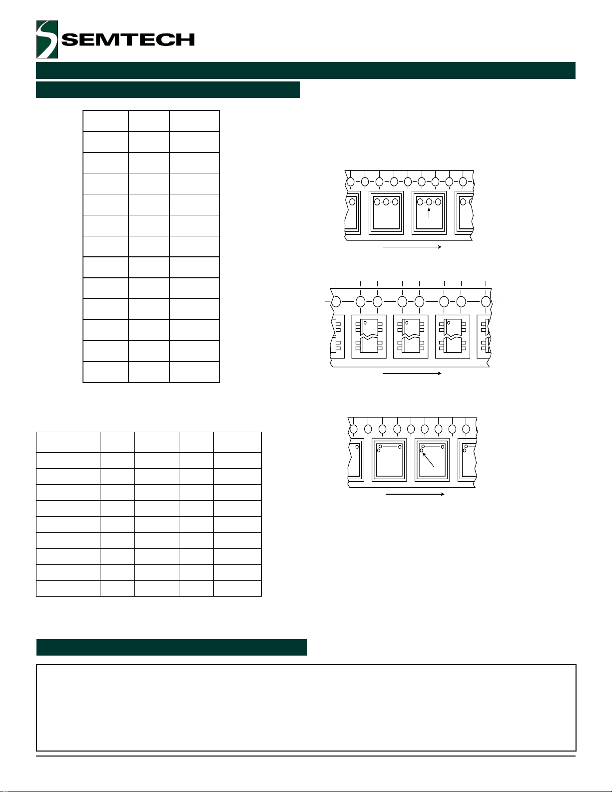
Semtech's tape and reel packaging fully conforms to the latest EIA-481-1A and EIA-481-2A specifications.
The antistatic embossed tape provides a secure cavity sealed with a peel-back cover tape.
Typical
+ + + + + + + + + +
PLCC Devices
SOIC & MSOP
Devices
PIN 1
Linear Direction of Travel
Typical
+ + + + + + +
+
Linear Direction of Travel
Typical
+ + ++ + ++ + ++ + +
View from
Tape Side
View from
Tape Side
epyTeciveD
82-CCLP420573173
8-CIOS21005,23189
61-CIOS61005,23194
02-CIOS42000,13183
8-POSM21005,23105
01-POSM21005,23105
)mm7x7(23-PFQL61000,131)yart(052
)mm7x7(23-PFQT61000,131)yart(052
)mm5x5(23-PFQT61000,131)yart(063
htdiWepaT
)mm(
xaM
leeR/eciveD
eziSleeR
)hcni(
Contact Information
Division Headquarters
10021 Willow Creek Road
San Diego, CA 92131
Phone (858) 695-1808
FAX (858)695-2633
High-Performance Products Division
xaM
ebuT/eciveD
LQFP & TQFP
Devices
+ + + + + + + + + +
+ +
Ordering Information
To order devices which are to be delivered in Tape and Reel, add the suffix T to the
device number being ordered.
Semtech Corporation
++
+
Linear Direction of Travel
+
PIN 1
+
+
+
View from
Tape Side
Marketing Group
1111 Comstock Street
Santa Clara, CA 95054
Phone: (408) 566-8776
FAX: (408) 727-8994
Revision 1/January 23, 2001
30
www.semtech.com
 Loading...