

Page 1

DATA SH EET
Product specification
Supersedes data of 1999 Aug 17
File under Integrated Circuits, IC18
2000 Jan 04
INTEGRATED CIRCUITS
SJA1000
Stand-alone CAN controller
Page 2

2000 Jan 04 2
Philips Semiconductors Product specification
Stand-alone CAN controller SJA1000
CONTENTS
1 FEATURES
2 GENERAL DESCRIPTION
3 ORDERING INFORMATION
4 BLOCK DIAGRAM
5 PINNING
6 FUNCTIONAL DESCRIPTION
6.1 Description of the CAN controller blocks
6.1.1 Interface Management Logic (IML)
6.1.2 Transmit Buffer (TXB)
6.1.3 Receive Buffer (RXB, RXFIFO)
6.1.4 Acceptance Filter (ACF)
6.1.5 Bit Stream Processor (BSP)
6.1.6 Bit Timing Logic (BTL)
6.1.7 Error Management Logic (EML)
6.2 Detailed description of the CAN controller
6.2.1 PCA82C200 compatibility
6.2.2 Differences between BasicCAN and PeliCAN
mode
6.3 BasicCAN mode
6.3.1 BasicCAN address layout
6.3.2 Reset values
6.3.3 Control Register (CR)
6.3.4 Command Register (CMR)
6.3.5 Status Register (SR)
6.3.6 Interrupt Register (IR)
6.3.7 Transmit buffer layout
6.3.8 Receive buffer
6.3.9 Acceptance filter
6.4 PeliCAN mode
6.4.1 PeliCAN address layout
6.4.2 Reset values
6.4.3 Mode Register (MOD)
6.4.4 Command Register (CMR)
6.4.5 Status Register (SR)
6.4.6 Interrupt Register (IR)
6.4.7 Interrupt Enable Register (IER)
6.4.8 Arbitration Lost Capture register (ALC)
6.4.9 Error Code Capture register (ECC)
6.4.10 Error Warning Limit Register (EWLR)
6.4.11 RX Error Counter Register (RXERR)
6.4.12 TX Error Counter Register (TXERR)
6.4.13 Transmit buffer
6.4.14 Receive buffer
6.4.15 Acceptance filter
6.4.16 RX Message Counter (RMC)
6.4.17 RX Buffer Start Address register (RBSA)
6.5 Common registers
6.5.1 Bus Timing Register 0 (BTR0)
6.5.2 Bus Timing Register 1 (BTR1)
6.5.3 Output Control Register (OCR)
6.5.4 Clock Divider Register (CDR)
7 LIMITING VALUES
8 THERMAL CHARACTERISTICS
9 DC CHARACTERISTICS
10 AC CHARACTERISTICS
10.1 AC timing diagrams
10.2 Additional AC information
11 PACKAGE OUTLINES
12 SOLDERING
12.1 Introduction
12.2 DIP
12.2.1 Soldering by dipping or by wave
12.2.2 Repairing soldered joints
12.3 SO
12.3.1 Reflow soldering
12.3.2 Wave soldering
12.3.3 Repairing soldered joints
13 DEFINITIONS
14 LIFE SUPPORT APPLICATIONS
Page 3

2000 Jan 04 3
Philips Semiconductors Product specification
Stand-alone CAN controller SJA1000
1 FEATURES
• Pin compatibility to the PCA82C200 stand-alone CAN
controller
• Electrical compatibility to the PCA82C200 stand-alone
CAN controller
• PCA82C200 mode (BasicCAN mode is default)
• Extended receive buffer (64-byte FIFO)
• CAN 2.0B protocol compatibility (extended frame
passive in PCA82C200 compatibility mode)
• Supports 11-bit identifier as well as 29-bit identifier
• Bit rates up to 1 Mbits/s
• PeliCAN mode extensions:
– Error counters with read/write access
– Programmable error warning limit
– Last error code register
– Error interrupt for each CAN-bus error
– Arbitration lost interrupt with detailed bit position
– Single-shot transmission (no re-transmission)
– Listen only mode (no acknowledge, no active error
flags)
– Hot plugging support (software driven bit rate
detection)
– Acceptance filter extension (4-byte code, 4-byte
mask)
– Reception of‘own’ messages (self reception request)
• 24 MHz clock frequency
• Interfaces to a variety of microprocessors
• Programmable CAN output driver configuration
• Extended ambient temperature range (−40 to +125 °C).
2 GENERAL DESCRIPTION
The SJA1000 is a stand-alone controller for the Controller
Area Network (CAN) used within automotive and general
industrial environments. It is the successor of the
PCA82C200 CAN controller (BasicCAN) from Philips
Semiconductors. Additionally, a new mode of operation is
implemented (PeliCAN) which supports the CAN 2.0B
protocol specification with several new features.
3 ORDERING INFORMATION
TYPE NUMBER
PACKAGE
NAME DESCRIPTION VERSION
SJA1000 DIP28 plastic dual in-line package; 28 leads (600 mil) SOT117-1
SJA1000T SO28 plastic small outline package; 28 leads; body width 7.5 mm SOT136-1
Page 4
2000 Jan 04 4
Philips Semiconductors Product specification
Stand-alone CAN controller SJA1000
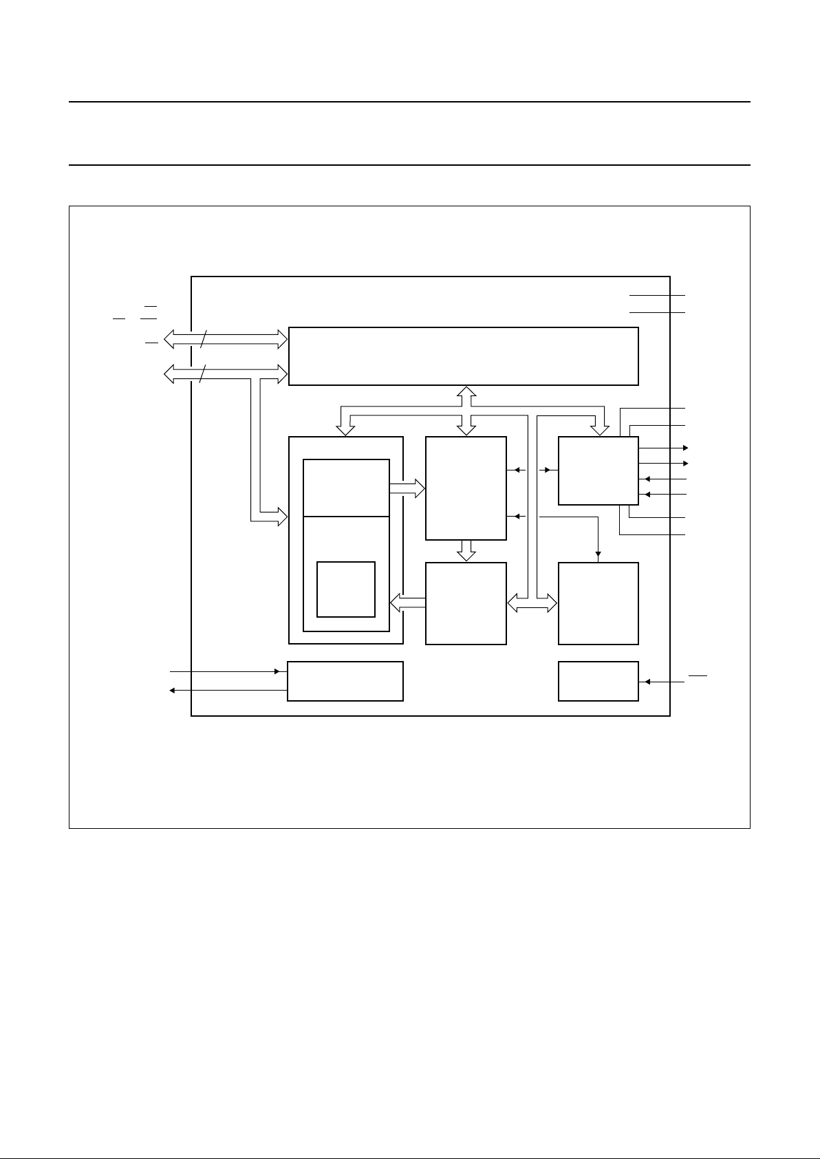
4 BLOCK DIAGRAM
Fig.1 Block diagram.
handbook, full pagewidth
MGK623
INTERFACE MANAGEMENT LOGIC
7
8
address/data
control
MESSAGE BUFFER
TRANSMIT
BUFFER
RECEIVE
BUFFER
RECEIVE
FIFO
BIT
STREAM
PROCESSOR
ACCEPTANCE
FILTER
BIT TIMING
LOGIC
ERROR
MANAGEMENT
LOGIC
RESETOSCILLATOR
XTAL1
9
XTAL2
10
TX0
TX1
RX0
RX1
17
18
21
20
19
14
13
15
12
8
22
internal bus
V
DD3
V
SS3
V
DD1
V
SS1
V
SS2
V
DD2
AD7 to AD0
2, 1,
28 to 23
3 to 7,
11, 16
ALE/AS, CS,
RD/E, WR,
CLKOUT,
MODE, INT
RST
SJA1000
Page 5

2000 Jan 04 5
Philips Semiconductors Product specification
Stand-alone CAN controller SJA1000
5 PINNING
Note
1. XTAL1 and XTAL2 pins should be connected to V
SS1
via 15 pF capacitors.
SYMBOL PIN DESCRIPTION
AD7 to AD0 2, 1, 28 to 23 multiplexed address/data bus
ALE/AS 3 ALE input signal (Intel mode), AS input signal (Motorola mode)
CS 4 chip select input, LOW level allows access to the SJA1000
RD/E 5 RD signal (Intel mode) or E enable signal (Motorola mode) from the microcontroller
WR 6 WR signal (Intel mode) or RD/WR signal (Motorola mode) from the microcontroller
CLKOUT 7 clock output signal produced by the SJA1000 for the microcontroller; the clock
signal is derived from the built-in oscillator via the programmable divider; the clock
off bit within the clock divider register allows this pin to disable
V
SS1
8 ground for logic circuits
XTAL1 9 input to the oscillator amplifier; external oscillator signal is input via this pin; note 1
XTAL2 10 output from the oscillator amplifier; the output must be left open-circuit when an
external oscillator signal is used; note 1
MODE 11 mode select input
1 = selects Intel mode
0 = selects Motorola mode
V
DD3
12 5 V supply for output driver
TX0 13 output from the CAN output driver 0 to the physical bus line
TX1 14 output from the CAN output driver 1 to the physical bus line
V
SS3
15 ground for output driver
INT 16 interrupt output, used to interrupt the microcontroller; INT is active LOW if any bit of
the internal interrupt register is set; INT is an open-drain output and is designed to
be a wired-OR with other INT outputs within the system; a LOW level on this pin will
reactivate the IC from sleep mode
RST 17 reset input, used to reset the CAN interface (active LOW);automatic power-on reset
can be obtained by connecting RST via a capacitor to VSS and a resistor to V
DD
(e.g. C = 1 µF; R = 50 kΩ)
V
DD2
18 5 V supply for input comparator
RX0, RX1 19, 20 input from the physical CAN-bus line to the input comparator of the SJA1000;
a dominant level will wake up the SJA1000 if sleeping; a dominant level is read, if
RX1 is higher than RX0 and vice versa for the recessive level; if the CBP bit (see
Table 49) is set in the clock divider register, the CAN input comparator is bypassed
to achieve lower internal delays if an external transceiver circuitry is connected to
the SJA1000; in this case only RX0 is active; HIGH is interpreted as recessive level
and LOW is interpreted as dominant level
V
SS2
21 ground for input comparator
V
DD1
22 5 V supply for logic circuits
Page 6
2000 Jan 04 6
Philips Semiconductors Product specification
Stand-alone CAN controller SJA1000
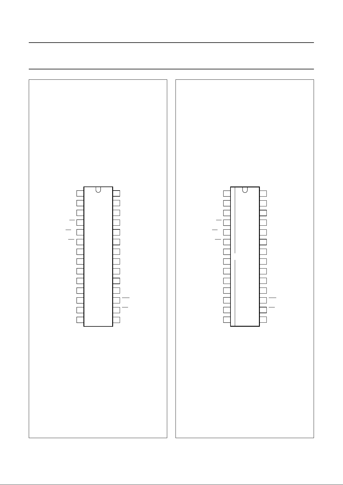
Fig.2 Pin configuration (DIP28).
handbook, halfpage
AD6
AD7
ALE/AS
CLKOUT
V
SS1
XTAL1
XTAL2
MODE
V
DD3
TX0
TX1
AD5
AD4
AD3
AD2
AD0
V
DD1
AD1
V
SS2
RX1
RX0
V
DD2
RST
INT
V
SS3
1
2
3
4
5
6
7
8
9
10
11
12
13
28
27
26
25
24
23
22
21
20
19
18
17
16
1514
SJA1000
MGK616
CS
RD/E
WR
Fig.3 Pin configuration (SO28).
handbook, halfpage
AD6
AD7
ALE/AS
CLKOUT
V
SS1
XTAL1
XTAL2
MODE
V
DD3
TX0
TX1
AD5
AD4
AD3
AD2
AD0
V
DD1
AD1
V
SS2
RX1
RX0
V
DD2
RST
INT
V
SS3
1
2
3
4
5
6
7
8
9
10
11
12
13
28
27
26
25
24
23
22
21
20
19
18
17
16
1514
SJA1000T
MGK617
CS
RD/E
WR
Page 7

2000 Jan 04 7
Philips Semiconductors Product specification
Stand-alone CAN controller SJA1000
6 FUNCTIONAL DESCRIPTION
6.1 Description of the CAN controller blocks
6.1.1 INTERFACE MANAGEMENT LOGIC (IML)
The interface management logic interprets commands
from the CPU, controls addressing of the CAN registers
and provides interrupts and status information to the host
microcontroller.
6.1.2 TRANSMIT BUFFER (TXB)
The transmit buffer is an interface between the CPU and
the Bit Stream Processor (BSP) that is able to store a
complete message for transmission over the CAN
network. The buffer is 13 bytes long, written to by the CPU
and read out by the BSP.
6.1.3 RECEIVE BUFFER (RXB, RXFIFO)
The receive buffer is an interface between the acceptance
filter and the CPU that stores the received and accepted
messages from the CAN-bus line. The Receive Buffer
(RXB)representsaCPU-accessible13-bytewindowof the
Receive FIFO (RXFIFO), which has a total length of
64 bytes.
With the help of this FIFO the CPU is able to process one
message while other messages are being received.
6.1.4 ACCEPTANCE FILTER (ACF)
Theacceptance filter compares the receivedidentifierwith
the acceptance filter register contents and decides
whether this message should be accepted or not. In the
eventofapositiveacceptancetest, the complete message
is stored in the RXFIFO.
6.1.5 BIT STREAM PROCESSOR (BSP)
Thebitstreamprocessorisasequencerwhichcontrols the
data stream between the transmit buffer, RXFIFO and the
CAN-bus. It also performs the error detection, arbitration,
stuffing and error handling on the CAN-bus.
6.1.6 BIT TIMING LOGIC (BTL)
The bit timing logic monitors the serial CAN-bus line and
handlesthe bus line-related bit timing. It issynchronized to
the bit stream on the CAN-bus on a
‘recessive-to-dominant’bus line transition at the beginning
of a message (hard synchronization) and re-synchronized
on further transitions during the reception of a message
(soft synchronization). The BTL also provides
programmable time segments to compensate for the
propagation delay times and phase shifts (e.g. due to
oscillator drifts) and to define the sample point and the
number of samples to be taken within a bit time.
6.1.7 ERROR MANAGEMENT LOGIC (EML)
The EML is responsible for the error confinement of the
transfer-layer modules. It receives error announcements
from the BSP and then informs the BSP and IML about
error statistics.
6.2 Detailed description of the CAN controller
The SJA1000 is designed to be software and
pin-compatible to its predecessor, the PCA82C200
stand-alone CAN controller. Additionally, a lot of new
functions are implemented. To achieve the software
compatibility, two different modes of operation are
implemented:
• BasicCAN mode; PCA82C200 compatible
• PeliCAN mode; extended features.
The mode of operation is selected with the CAN-mode bit
located within the clock divider register. Default mode
upon reset is the BasicCAN mode.
6.2.1 PCA82C200 COMPATIBILITY
In BasicCAN mode the SJA1000 emulates all known
registers from the PCA82C200 stand-alone CAN
controller. The characteristics, as described in Sections
6.2.1.1 to 6.2.1.4 are different from the PCA82C200
design with respect to software compatibility.
6.2.1.1 Synchronization mode
The SYNC bit in the control register is removed (CR.6 in
the PCA82C200). Synchronization is only possible by a
recessive-to-dominant transition on the CAN-bus. Writing
tothis bit has no effect. Toachieve compatibility to existing
application software, a read access to this bit will reflect
the previously written value (flip-flop without effect).
6.2.1.2 Clock divider register
The clock divider register is used to select the CAN mode
of operation (BasicCAN/PeliCAN). Therefore one of the
reserved bits within the PCA82C200 is used. Writing a
value between 0 and 7, as allowed for the PCA82C200,
will enter the BasicCAN mode. The default state is divide
by 12 for Motorola mode and divide by 2 for Intel mode.
An additionalfunctionis implemented within another of the
reserved bits. Setting of bit CBP (see Table 49) enables
the internal RX input comparator to be bypassed thereby
reducing the internal delays if an external transceiver
circuit is used.
Page 8

2000 Jan 04 8
Philips Semiconductors Product specification
Stand-alone CAN controller SJA1000
6.2.1.3 Receive buffer
The dual receive buffer concept of the PCA82C200 is
replaced by the receive FIFO from the PeliCAN controller.
Thishasnoeffecttotheapplication software except for the
data overrun probability. Now more than two messages
may be received (up to 64 bytes) until a data overrun
occurs.
6.2.1.4 CAN 2.0B
The SJA1000 is designed to support the full CAN 2.0B
protocol specification, which means that the extended
oscillator tolerance is implemented as well as the
processing of extended frame messages. In BasicCAN
mode it is possible to transmit and receive standard frame
messages only (11-bit identifier). If extended frame
messages (29-bit identifier) are detected on the CAN-bus,
they are tolerated and an acknowledge is given if the
message was correct, but there is no receive interrupt
generated.
6.2.2 DIFFERENCES BETWEEN BASICCAN AND PELICAN
MODE
In the PeliCAN mode the SJA1000 appears with a
re-organized register mapping with a lot of new features.
All known bits from the PCA82C200 design are available
as well as several new ones. In the PeliCAN mode the
complete CAN 2.0B functionality is supported (29-bit
identifier).
Main new features of the SJA1000 are:
• Reception and transmission of standard and extended
frame format messages
• Receive FIFO (64-byte)
• Single/dual acceptance filter with mask and code
register for standard and extended frame
• Error counters with read/write access
• Programmable error warning limit
• Last error code register
• Error interrupt for each CAN-bus error
• Arbitration lost interrupt with detailed bit position
• Single-shot transmission (no re-transmission on error or
arbitration lost)
• Listen only mode (monitoring of the CAN-bus, no
acknowledge, no error flags)
• Hot plugging supported (disturbance-free software
driven bit rate detection)
• Disable CLKOUT by hardware.
6.3 BasicCAN mode
6.3.1 BASICCAN ADDRESS LAYOUT
The SJA1000 appears to a microcontroller as a
memory-mapped I/O device. An independent operation of
both devices is guaranteed by a RAM-like implementation
of the on-chip registers.
The address area of the SJA1000 consists of the control
segment and the message buffers. The control segmentis
programmed during an initialization download in order to
configure communication parameters (e.g. bit timing).
Communication over the CAN-bus is also controlled via
this segment by the microcontroller. During initialization
the CLKOUT signal may be programmed to a value
determined by the microcontroller.
A message, which should be transmitted, has tobe written
to the transmit buffer. After a successful reception the
microcontroller may read the received message from the
receive buffer and then release it for further use.
The exchange of status, control and command signals
between the microcontroller and the SJA1000 is
performed in the control segment. The layout of this
segment is shown in Table 3. After an initial download, the
contents of the registers acceptance code, acceptance
mask, bus timing registers 0 and 1 and output control
should not be changed. Therefore these registers may
only be accessed when the reset request bit in the control
register is set HIGH.
For register access, two different modes have to be
distinguished:
• Reset mode
• Operating mode.
The reset mode (see Table 3, control register, bit Reset
Request) is entered automatically after a hardware reset
or when the controller enters the bus-off state (see
Table 5, status register, bit Bus Status). The operating
modeisactivatedby resetting of the reset request bit in the
control register.
Page 9

2000 Jan 04 9
Philips Semiconductors Product specification
Stand-alone CAN controller SJA1000
Table 1 BasicCAN address allocation; note 1
Notes
1. It should be noted that the registers are repeated within higher CAN address areas (the most significant bits of the
8-bit CPU address are not decoded: CAN address 32 continues with CAN address 0 and so on).
2. Test register is used for production testing only. Using this register during normal operation may result in undesired
behaviour of the device.
3. Some bits are writeable in reset mode only (CAN mode and CBP).
CAN
ADDRESS
SEGMENT
OPERATING MODE RESET MODE
READ WRITE READ WRITE
0 control control control control control
1 (FFH) command (FFH) command
2 status − status −
3 interrupt − interrupt −
4 (FFH) − acceptance code acceptance code
5 (FFH) − acceptance mask acceptance mask
6 (FFH) − bus timing 0 bus timing 0
7 (FFH) − bus timing 1 bus timing 1
8 (FFH) − output control output control
9 test test; note 2 test test; note 2
10 transmit
buffer
identifier (10 to 3) identifier (10 to 3) (FFH) −
11 identifier (2 to 0),
RTR and DLC
identifier (2 to 0),
RTR and DLC
(FFH) −
12 data byte 1 data byte 1 (FFH) −
13 data byte 2 data byte 2 (FFH) −
14 data byte 3 data byte 3 (FFH) −
15 data byte 4 data byte 4 (FFH) −
16 data byte 5 data byte 5 (FFH) −
17 data byte 6 data byte 6 (FFH) −
18 data byte 7 data byte 7 (FFH) −
19 data byte 8 data byte 8 (FFH) −
20 receive
buffer
identifier (10 to 3) identifier (10 to 3) identifier (10 to 3) identifier (10 to 3)
21 identifier (2 to 0),
RTR and DLC
identifier (2 to 0),
RTR and DLC
identifier (2 to 0),
RTR and DLC
identifier (2 to 0),
RTR and DLC
22 data byte 1 data byte 1 data byte 1 data byte 1
23 data byte 2 data byte 2 data byte 2 data byte 2
24 data byte 3 data byte 3 data byte 3 data byte 3
25 data byte 4 data byte 4 data byte 4 data byte 4
26 data byte 5 data byte 5 data byte 5 data byte 5
27 data byte 6 data byte 6 data byte 6 data byte 6
28 data byte 7 data byte 7 data byte 7 data byte 7
29 data byte 8 data byte 8 data byte 8 data byte 8
30 (FFH) − (FFH) −
31 clock divider clock divider; note 3 clock divider clock divider
Page 10

2000 Jan 04 10
Philips Semiconductors Product specification
Stand-alone CAN controller SJA1000
6.3.2 RESET VALUES
Detection of a ‘reset request’ results in aborting the current transmission/reception of a message and entering the reset
mode. On the ‘1-to-0’ transition of the reset request bit, the CAN controller returns to the operating mode.
Table 2 Reset mode configuration; notes 1 and 2
REGISTER BIT SYMBOL NAME
VALUE
RESET BY
HARDWARE
SETTING
BIT CR.0 BY
SOFTWAREOR
DUE TO
BUS-OFF
Control CR.7 − reserved 0 0
CR.6 − reserved X X
CR.5 − reserved 1 1
CR.4 OIE Overrun Interrupt Enable X X
CR.3 EIE Error Interrupt Enable X X
CR.2 TIE Transmit Interrupt Enable X X
CR.1 RIE Receive Interrupt Enable X X
CR.0 RR Reset Request 1 (reset mode) 1 (reset mode)
Command CMR.7 − reserved note 3 note 3
CMR.6 − reserved
CMR.5 − reserved
CMR.4 GTS Go To Sleep
CMR.3 CDO Clear Data Overrun
CMR.2 RRB Release Receive Buffer
CMR.1 AT Abort Transmission
CMR.0 TR Transmission Request
Status SR.7 BS Bus Status 0 (bus-on) X
SR.6 ES Error Status 0 (ok) X
SR.5 TS Transmit Status 0 (idle) 0 (idle)
SR.4 RS Receive Status 0 (idle) 0 (idle)
SR.3 TCS Transmission Complete Status 1 (complete) X
SR.2 TBS Transmit Buffer Status 1 (released) 1 (released)
SR.1 DOS Data Overrun Status 0 (absent) 0 (absent)
SR.0 RBS Receive Buffer Status 0 (empty) 0 (empty)
Interrupt IR.7 − reserved 1 1
IR.6 − reserved 1 1
IR.5 − reserved 1 1
IR.4 WUI Wake-Up Interrupt 0 (reset) 0 (reset)
IR.3 DOI Data Overrun Interrupt 0 (reset) 0 (reset)
IR.2 EI Error Interrupt 0 (reset) X; note 4
IR.1 TI Transmit Interrupt 0 (reset) 0 (reset)
IR.0 RI Receive Interrupt 0 (reset) 0 (reset)
Page 11

2000 Jan 04 11
Philips Semiconductors Product specification
Stand-alone CAN controller SJA1000
Acceptance code AC.7 to 0 AC Acceptance Code X X
Acceptance mask AM.7 to 0 AM Acceptance Mask X X
Bus timing 0 BTR0.7 SJW.1 Synchronization Jump Width 1 X X
BTR0.6 SJW.0 Synchronization Jump Width 0 X X
BTR0.5 BRP.5 Baud Rate Prescaler 5 X X
BTR0.4 BRP.4 Baud Rate Prescaler 4 X X
BTR0.3 BRP.3 Baud Rate Prescaler 3 X X
BTR0.2 BRP.2 Baud Rate Prescaler 2 X X
BTR0.1 BRP.1 Baud Rate Prescaler 1 X X
BTR0.0 BRP.0 Baud Rate Prescaler 0 X X
Bus timing 1 BTR1.7 SAM Sampling X X
BTR1.6 TSEG2.2 Time Segment 2.2 X X
BTR1.5 TSEG2.1 Time Segment 2.1 X X
BTR1.4 TSEG2.0 Time Segment 2.0 X X
BTR1.3 TSEG1.3 Time Segment 1.3 X X
BTR1.2 TSEG1.2 Time Segment 1.2 X X
BTR1.1 TSEG1.1 Time Segment 1.1 X X
BTR1.0 TSEG1.0 Time Segment 1.0 X X
Output control OC.7 OCTP1 Output Control Transistor P1 X X
OC.6 OCTN1 Output Control Transistor N1 X X
OC.5 OCPOL1 Output Control Polarity 1 X X
OC.4 OCTP0 Output Control Transistor P0 X X
OC.3 OCTN0 Output Control Transistor N0 X X
OC.2 OCPOL0 Output Control Polarity 0 X X
OC.1 OCMODE1 Output Control Mode 1 X X
OC.0 OCMODE0 Output Control Mode 0 X X
Transmit buffer − TXB Transmit Buffer X X
Receive buffer − RXB Receive Buffer X; note 5 X; note 5
Clock divider − CDR Clock Divider Register 00000000
(Intel);
00000101
(Motorola)
X
REGISTER BIT SYMBOL NAME
VALUE
RESET BY
HARDWARE
SETTING
BIT CR.0 BY
SOFTWAREOR
DUE TO
BUS-OFF
Page 12

2000 Jan 04 12
Philips Semiconductors Product specification
Stand-alone CAN controller SJA1000
Notes
1. X means that the value of these registers or bits is not influenced.
2. Remarks in brackets explain functional meaning.
3. Reading the command register will always reflect a binary ‘11111111’.
4. On bus-off the error interrupt is set, if enabled.
5. Internal read/write pointers of the RXFIFO are reset to their initial values. A subsequent read access to the RXB
would show undefined data values (parts of old messages). If a message is transmitted, this message is written in
parallel to the receive buffer but no receive interrupt is generated and the receive buffer area is not locked. So, even
if the receive buffer is empty, the last transmitted message may be read from the receive buffer until it is overridden
by the next received or transmitted message.
Upon a hardware reset, the RXFIFO pointers are reset to the physical RAM address ‘0’. Setting CR.0 by software or
due to the bus-off event will reset the RXFIFO pointers to the currently valid FIFO start address which is different
from the RAM address ‘0’ after the first release receive buffer command.
6.3.3 CONTROL REGISTER (CR)
The contents of the control register are used to change the behaviour of the CAN controller. Bits may be set or reset by
the attached microcontroller which uses the control register as a read/write memory.
Table 3 Bit interpretation of the control register (CR); CAN address 0
BIT SYMBOL NAME VALUE FUNCTION
CR.7 −− −reserved; note 1
CR.6 −− −reserved; note 2
CR.5 −− −reserved; note 3
CR.4 OIE Overrun Interrupt Enable 1 enabled; if the data overrun bit is set, the
microcontroller receives an overrun interrupt
signal (see also status register; Table 5)
0 disabled; the microcontroller receives no overrun
interrupt signal from the SJA1000
CR.3 EIE Error Interrupt Enable 1 enabled; if the error or bus status change, the
microcontroller receives an error interrupt signal
(see also status register; Table 5)
0 disabled; the microcontroller receives no error
interrupt signal from the SJA1000
CR.2 TIE Transmit Interrupt Enable 1 enabled; when a message has been successfully
transmitted or the transmit buffer is accessible
again, (e.g. after an abort transmission command)
the SJA1000 transmits a transmit interrupt signal
to the microcontroller
0 disabled; the microcontroller receives no transmit
interrupt signal from the SJA1000
Page 13

2000 Jan 04 13
Philips Semiconductors Product specification
Stand-alone CAN controller SJA1000
Notes
1. Any write access to the control register has to set this bit to logic 0 (reset value is logic 0).
2. In the PCA82C200 this bit was used to select the synchronization mode. Because this mode is not longer
implemented, setting this bit has no influence on the microcontroller. Due to software compatibility setting this bit is
allowed. This bit will not change after hardware or software reset. In addition the value written by users software is
reflected.
3. Reading this bit will always reflect a logic 1.
4. During a hardware reset or when the bus status bit is set to logic 1 (bus-off), the reset request bit is set to logic 1
(present). If this bit is accessed by software, a value change will become visible and takes effect first with the next
positiveedge of the internal clock whichoperateswith1⁄2ofthe external oscillator frequency. During anexternalreset
the microcontroller cannot set the reset request bit to logic 0 (absent). Therefore, after having set the reset request
bit to logic 0, the microcontroller must check this bit to ensure that the external reset pin is not being held LOW.
Changes of the reset request bit are synchronized with the internal divided clock. Reading the reset request bit
reflects the synchronized status.
After the reset request bit is set to logic 0 the SJA1000 will wait for:
a) One occurrence of bus-free signal (11 recessive bits), if the preceding reset request has been caused by a
hardware reset or a CPU-initiated reset
b) 128 occurrencesof bus-free, if the preceding resetrequesthas been caused by a CAN controllerinitiated bus-off,
before re-entering the bus-on mode; it should be noted that several registers are modified if the reset request bit
was set (see also Table 2).
6.3.4 COMMAND REGISTER (CMR)
A command bit initiates an action within the transfer layer of the SJA1000. The command register appears to the
microcontroller as a write only memory. If a read access is performed to this address the byte ‘11111111’ is returned.
Between two commands at least one internal clock cycle is needed to process. The internal clock is divided by two from
the external oscillator frequency.
CR.1 RIE Receive Interrupt Enable 1 enabled; when a message has been received
without errors, the SJA1000 transmits a receive
interrupt signal to the microcontroller
0 disabled; the microcontroller receives no transmit
interrupt signal from the SJA1000
CR.0 RR Reset Request; note 4 1 present; detection of a reset request results in
aborting the current transmission/reception of a
message and entering the reset mode
0 absent; on the ‘1-to-0’ transition of the reset
request bit, the SJA1000 returns to the operating
mode
BIT SYMBOL NAME VALUE FUNCTION
Page 14

2000 Jan 04 14
Philips Semiconductors Product specification
Stand-alone CAN controller SJA1000
Table 4 Bit interpretation of the command register (CMR); CAN address 1
Notes
1. The SJA1000 will enter sleep mode if the sleep bit is set to logic 1 (sleep); there is no bus activity and no interrupt is
pending. Setting of GTS with at least one of the previously mentioned exceptions valid will result in a wake-up
interrupt. After sleep mode is set, the CLKOUT signal continues until at least 15 bit times have passed, to allow a
host microcontroller clocked via this signal to enter its own standby mode before the CLKOUT goes LOW.
The SJA1000 will wake up when one of the three previously mentioned conditions is negated: after ‘Go To Sleep’ is
set LOW (wake-up), there is bus activity or
INT is driven LOW (active). On wake-up, the oscillator is started and a
wake-up interrupt is generated. A sleeping SJA1000 which wakes up due to bus activity will not be able to receive
thismessageuntilit detects 11 consecutive recessive bits (bus-free sequence). It should be noted thatsettingofGTS
isnotpossiblein reset mode. After clearing of reset request, setting ofGTSispossiblefirst, when bus-free is detected
again.
2. This command bit is used to clear the data overrun condition indicated by the data overrun status bit. As long as the
data overrun status bit is set no further data overrun interrupt is generated. It is allowed to give the clear data overrun
command at the same time as a release receive buffer command.
3. After reading the contents of the receive buffer, the microcontroller can release this memory space of the RXFIFO
by setting the release receive buffer bit to logic 1. This may result in another message becoming immediately
available within the receive buffer. This event will force another receive interrupt, if enabled. If there is no other
message available no further receive interrupt is generated and the receive buffer status bit is cleared.
4. The abort transmission bit is used when the CPU requires the suspension of the previously requested transmission,
e.g. to transmit a more urgent message before. A transmission already in progress is not stopped. In order to see if
the original message had been either transmitted successfully or aborted, the transmission complete status bit
should be checked. This should be done after the transmit buffer status bit has been set to logic 1 (released) or a
transmit interrupt has been generated.
5. If the transmission request was set to logic 1 in a previous command, it cannot be cancelled by setting the
transmission request bit to logic 0. The requested transmission may be cancelled by setting the abort transmission
bit to logic 1.
BIT SYMBOL NAME VALUE FUNCTION
CMR.7 −− −reserved
CMR.6 −− −reserved
CMR.5 −− −reserved
CMR.4 GTS Go To Sleep; note 1 1 sleep; the SJA1000 enters sleep mode if no CAN
interrupt is pending and there is no bus activity
0 wake up; SJA1000 operates normal
CMR.3 CDO Clear Data Overrun;
note 2
1 clear; data overrun status bit is cleared
0 no action
CMR.2 RRB Release Receive Buffer;
note 3
1 released; the receive buffer, representing the
message memory space in the RXFIFO is
released
0 no action
CMR.1 AT Abort Transmission;
note 4
1 present; if not already in progress, a pending
transmission request is cancelled
0 absent; no action
CMR.0 TR Transmission Request;
note 5
1 present; a message will be transmitted
0 absent; no action
Page 15

2000 Jan 04 15
Philips Semiconductors Product specification
Stand-alone CAN controller SJA1000
6.3.5 STATUS REGISTER (SR)
The content of the status register reflects the status of the SJA1000. The status register appears to the microcontroller
as a read only memory.
Table 5 Bit interpretation of the status register (SR); CAN address 2
BIT SYMBOL NAME VALUE FUNCTION
SR.7 BS Bus Status; note 1 1 bus-off; the SJA1000 is not involved in bus
activities
0 bus-on; the SJA1000 is involved in bus activities
SR.6 ES Error Status; note 2 1 error; at least one of the error counters has
reached or exceeded the CPU warning limit
0 ok; both error counters are below the warning limit
SR.5 TS Transmit Status; note 3 1 transmit; the SJA1000 is transmitting a message
0 idle; no transmit message is in progress
SR.4 RS Receive Status; note 3 1 receive; the SJA1000 is receiving a message
0 idle; no receive message is in progress
SR.3 TCS Transmission Complete
Status; note 4
1 complete; the last requested transmission has
been successfully completed
0 incomplete; the previouslyrequestedtransmission
is not yet completed
SR.2 TBS Transmit Buffer Status;
note 5
1 released; the CPU may write a message into the
transmit buffer
0 locked; the CPU cannot access the transmit
buffer; a message is waiting for transmission or is
already in process
SR.1 DOS Data Overrun Status;
note 6
1 overrun; a message was lost because there was
not enough space for that message in the RXFIFO
0 absent; no data overrun has occurred since the
last clear data overrun command was given
SR.0 RBS Receive Buffer Status;
note 7
1 full; one or more messages are available in the
RXFIFO
0 empty; no message is available
Page 16

2000 Jan 04 16
Philips Semiconductors Product specification
Stand-alone CAN controller SJA1000
Notes
1. When the transmit error counter exceeds the limit of 255 [the bus status bit is set to logic 1 (bus-off)] the
CAN controller will set the reset request bit to logic 1 (present) and an error interrupt is generated, if enabled. It will
stay in this mode until the CPU clears the reset request bit. Once this is completed the CAN controller will wait the
minimum protocol-defined time (128 occurrences of the bus-free signal). After that the bus status bit is cleared
(bus-on), the error status bit is set to logic 0 (ok), the error counters are reset and an error interrupt is generated, if
enabled.
2. Errors detected during reception or transmission will affect the error counters according to the CAN 2.0B protocol
specification. The error status bit is set when at least one of the error counters has reached or exceeded the CPU
warning limit of 96. An error interrupt is generated, if enabled.
3. If both the receive status and the transmit status bits are logic 0 (idle) the CAN-bus is idle.
4. The transmission complete status bit is set to logic 0 (incomplete) whenever the transmission request bit is set to
logic 1. The transmission complete status bit will remain at logic 0 (incomplete) until a message is transmitted
successfully.
5. If the CPU tries to write to the transmit buffer when the transmit buffer status bit is at logic 0 (locked), the written byte
will not be accepted and will be lost without being indicated.
6. When a message that shall be received has passed the acceptance filter successfully (i.e. earliest after arbitration
field), the CAN controller needs space in the RXFIFO to store the message descriptor. Accordingly there must be
enough space for each data byte which has been received. If there is not enough space to store the message, that
message will be dropped and the data overrun condition will be indicated to the CPU only, if this received message
has no errors until the last but one bit of end of frame (message becomes valid).
7. After reading a message stored in the RXFIFO and releasing this memory space with the command release receive
buffer, this bit is cleared. If there is another message available within the FIFO this bit is set again with the next bit
quantum (t
scl
).
Page 17

2000 Jan 04 17
Philips Semiconductors Product specification
Stand-alone CAN controller SJA1000
6.3.6 INTERRUPT REGISTER (IR)
The interrupt register allows the identification of an interrupt source. When one or more bits of this register are set, the
INT pin is activated (LOW). After this register is read by the microcontroller, all bits are reset what results in a floating
level at INT. The interrupt register appears to the microcontroller as a read only memory.
Table 6 Bit interpretation of the interrupt register (IR); CAN address 3
Notes
1. Reading this bit will always reflect a logic 1.
2. A wake-up interrupt is also generated if the CPU tries to set go to sleep while the CAN controller is involved in bus
activities or a CAN interrupt is pending.
3. The overrun interrupt bit (if enabled) and the data overrun status bit are set at the same time.
4. The receive interrupt bit (if enabled) and the receive buffer status bit are set at the same time.
It should be noted that the receive interrupt bit is cleared upon a read access, even if there is another message
available within the FIFO. The moment the release receive buffer command is given and there is another message
valid within the receive buffer, the receive interrupt is set again (if enabled) with the next t
scl
.
BIT SYMBOL NAME VALUE FUNCTION
IR.7 −− − reserved; note 1
IR.6 −− − reserved; note 1
IR.5 −− − reserved; note 1
IR.4 WUI Wake-Up Interrupt;
note 2
1 set; this bit is set when the sleep mode is left
0 reset; this bit is cleared by any read access of the
microcontroller
IR.3 DOI Data Overrun Interrupt;
note 3
1 set; this bit is set on a ‘0-to-1’ transition of the data
overrun status bit, when the data overrun interrupt
enable is set to logic 1 (enabled)
0 reset; this bit is cleared by any read access of the
microcontroller
IR.2 EI Error Interrupt 1 set; this bit is set on a change of either the error
status or bus status bits if the error interrupt
enable is set to logic 1 (enabled)
0 reset; this bit is cleared by any read access of the
microcontroller
IR.1 TI Transmit Interrupt 1 set; this bit is set whenever the transmit buffer
status changes from logic 0 to logic 1 (released)
and transmit interrupt enable is set to logic 1
(enabled)
0 reset; this bit is cleared by any read access of the
microcontroller
IR.0 RI Receive Interrupt; note 4 1 set; this bit is set while the receive FIFO is not
empty and the receive interrupt enable bit is set
to logic 1 (enabled)
0 reset; this bit is cleared by any read access of the
microcontroller
Page 18

2000 Jan 04 18
Philips Semiconductors Product specification
Stand-alone CAN controller SJA1000
6.3.7 TRANSMIT BUFFER LAYOUT
Theglobal layout of the transmit buffer is showninTable 7. The buffer serves to store amessagefrom the microcontroller
to be transmitted by the SJA1000. It is subdivided into a descriptor and data field. The transmit buffer can be written to
and read out by the microcontroller in operating mode only. In reset mode a ‘FFH’ is reflected for all bytes.
Table 7 Layout of transmit buffer
CAN
ADDRESS
FIELD NAME
BITS
76543210
10 descriptor identifier byte 1 ID.10 ID.9 ID.8 ID.7 ID.6 ID.5 ID.4 ID.3
11 identifier byte 2 ID.2 ID.1 ID.0 RTR DLC.3 DLC.2 DLC.1 DLC.0
12 data TX data 1 transmit data byte 1
13 TX data 2 transmit data byte 2
14 TX data 3 transmit data byte 3
15 TX data 4 transmit data byte 4
16 TX data 5 transmit data byte 5
17 TX data 6 transmit data byte 6
18 TX data 7 transmit data byte 7
19 TX data 8 transmit data byte 8
6.3.7.1 Identifier (ID)
The identifier consists of 11 bits (ID.10 to ID.0). ID.10 is
themostsignificant bit, which is transmitted first on thebus
during the arbitration process. The identifier acts as the
message’s name. It is used in a receiver for acceptance
filtering and also determining the bus access priority
during the arbitration process. The lower the binary value
of the identifier the higher the priority. This is due to a
larger number of leading dominant bits during arbitration.
6.3.7.2 Remote Transmission Request (RTR)
If this bit is set, a remote frame will be transmitted via the
bus.This means that nodata bytes are included withinthis
frame. Nevertheless, it is necessary to specify the correct
data length code which depends on the corresponding
data frame with the same identifier coding.
If the RTR bit is not set, a data frame will be sent including
the number of data bytes as specified by the data length
code.
6.3.7.3 Data Length Code (DLC)
The number of bytes in the data field of a message is
coded by the data length code. At the start of a remote
frame transmission the data length code is not considered
due to the RTR bit being at logic 1 (remote). This forces
the number of transmitted/received data bytes to be
logic 0. Nevertheless, the data length code must be
specified correctly to avoid bus errors if two
CAN controllersstartaremoteframetransmissionwiththe
same identifier simultaneously.
The range of the data byte count is 0 to 8 bytes and is
coded as follows:
DataByteCount = 8 × DLC.3 + 4 × DLC.2 + 2 × DLC.1 +
DLC.0
Forreasons of compatibility no datalengthcode >8 should
be used. If a value >8 is selected, 8 bytes are transmitted
in the data frame with the data length code specified in
DLC.
6.3.7.4 Data field
The number of transferred data bytes is determined by the
data length code. The first bit transmitted is the most
significant bit of data byte 1 at address 12.
6.3.8 RECEIVE BUFFER
The global layout of the receive buffer is very similar to the
transmit buffer described in Section 6.3.7. The receive
buffer is the accessible part of the RXFIFO and is located
in the range between CAN address 20 and 29.
Page 19
2000 Jan 04 19
Philips Semiconductors Product specification
Stand-alone CAN controller SJA1000
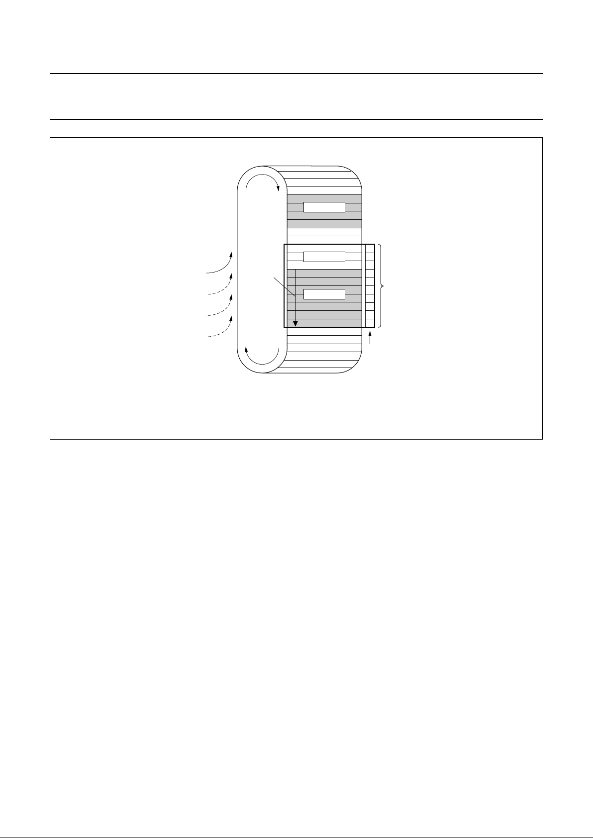
Fig.4 Example of the message storage within the RXFIFO.
Message 1 is now available in the receive buffer.
handbook, full pagewidth
MGK618
release
receive
buffer
command
64-byte
FIFO
incoming
messages
message 3
message 2
message 1
29
28
27
26
25
24
23
22
21
20
receive
buffer
window
CAN address
Identifier, remote transmission request bit and data length
code have the same meaning and location as described in
the transmit buffer but within the address range 20 to 29.
As illustrated in Fig.4 the RXFIFO has space for
64 message bytes in total. The number of messages that
can be stored in the FIFO at any particular moment
depends on the length of the individual messages. If there
is not enough space for a new message within the
RXFIFO, the CAN controller generates a data overrun
condition. A message which is partly written into the
RXFIFO, when the data overrun condition occurs, is
deleted. This situation is indicated to the microcontroller
via the status register and the data overrun interrupt, if
enabled and the frame was received without any errors
until the last but one bit of end of frame (RX message
becomes valid).
6.3.9 ACCEPTANCE FILTER
With the help of the acceptance filter the CAN controller is
abletoallow passing of received messages to the RXFIFO
only when the identifier bits of the received message are
equal to the predefined ones within the acceptance filter
registers. The acceptance filter is defined by the
acceptance code register (ACR; see Section 6.3.9.1) and
the acceptance mask register (AMR; see Section 6.3.9.2).
Page 20

2000 Jan 04 20
Philips Semiconductors Product specification
Stand-alone CAN controller SJA1000
6.3.9.1 Acceptance Code Register (ACR)
Table 8 ACR bit allocation; can address 4
BIT 7 BIT 6 BIT 5 BIT 4 BIT 3 BIT 2 BIT 1 BIT 0
AC.7 AC.6 AC.5 AC.4 AC.3 AC.2 AC.1 AC.0
This register can be accessed (read/write), if the reset
request bit is set HIGH (present). When a message is
received which passes the acceptance test and there is
receive buffer space left, then the respective descriptor
and data field are sequentially stored in the RXFIFO.
When the complete message has been correctly received
the following occurs:
• The receive status bit is set HIGH (full)
• If the receive interrupt enable bit is set HIGH (enabled),
the receive interrupt is set HIGH (set).
The acceptance code bits (AC.7 to AC.0) and the eight
most significant bits of the message’s identifier
(ID.10 to ID.3) must be equal to those bit positions which
are marked relevant by the acceptance mask bits
(AM.7 to AM.0). If the conditions as described in the
following equation are fulfilled, acceptance is given:
(ID.10 to ID.3) ≡ (AC.7 to AC.0)] ∨ (AM.7 to AM.0)
≡ 11111111
6.3.9.2 Acceptance Mask Register (AMR)
Table 9 AMR bit allocation; CAN address 5
BIT 7 BIT 6 BIT 5 BIT 4 BIT 3 BIT 2 BIT 1 BIT 0
AM.7 AM.6 AM.5 AM.4 AM.3 AM.2 AM.1 AM.0
This register can be accessed (read/write), if the reset
request bit is set HIGH (present). The acceptance mask
register qualifies which of the corresponding bits of the
acceptance code are ‘relevant’ (AM.X = 0) or ‘don’t care’
(AM.X = 1) for acceptance filtering.
6.3.9.3 Other registers
The other registers are described in Section 6.5.
6.4 PeliCAN mode
6.4.1 PELICAN ADDRESS LAYOUT
The CAN controller’s internal registers appear to the CPU
as on-chip memory mapped peripheralregisters. Because
the CAN controller can operate in different modes
(operating/reset; see also Section 6.4.3), one has to
distinguish between different internal address definitions.
Starting from CAN address 32 the complete internal RAM
(80-byte) is mapped to the CPU interface.
Page 21

2000 Jan 04 21
Philips Semiconductors Product specification
Stand-alone CAN controller SJA1000
Table 10 PeliCAN address allocation; note 1
CAN
ADDRESS
OPERATING MODE RESET MODE
READ WRITE READ WRITE
0 mode mode mode mode
1 (00H) command (00H) command
2 status − status −
3 interrupt − interrupt −
4 interrupt enable interrupt enable interrupt enable interrupt enable
5 reserved (00H) − reserved (00H) −
6 bus timing 0 − bus timing 0 bus timing 0
7 bus timing 1 − bus timing 1 bus timing 1
8 output control − output control output control
9 test test; note 2 test test; note 2
10 reserved (00H) − reserved (00H) −
11 arbitration lost capture − arbitration lost
capture
−
12 error code capture − error code
capture
−
13 error warning limit − error warning
limit
error warning
limit
14 RX error counter − RX error counter RX error counter
15 TX error counter − TX error counter TX error counter
16 RX frame
information
SFF; note 3
RX frame
information
EFF; note 4
TX frame
information
SFF; note 3
TX frame
information
EFF; note 4
acceptance
code 0
acceptance
code 0
17 RX identifier 1 RX identifier 1 TX identifier 1 TX identifier 1 acceptance
code 1
acceptance
code 1
18 RX identifier 2 RX identifier 2 TX identifier 2 TX identifier 2 acceptance
code 2
acceptance
code 2
19 RX data 1 RX identifier 3 TX data 1 TX identifier 3 acceptance
code 3
acceptance
code 3
20 RX data 2 RX identifier 4 TX data 2 TX identifier 4 acceptance
mask 0
acceptance
mask 0
21 RX data 3 RX data 1 TX data 3 TX data 1 acceptance
mask 1
acceptance
mask 1
22 RX data 4 RX data 2 TX data 4 TX data 2 acceptance
mask 2
acceptance
mask 2
23 RX data 5 RX data 3 TX data 5 TX data 3 acceptance
mask 3
acceptance
mask 3
24 RX data 6 RX data 4 TX data 6 TX data 4 reserved (00H) −
25 RX data 7 RX data 5 TX data 7 TX data 5 reserved (00H) −
26 RX data 8 RX data 6 TX data 8 TX data 6 reserved (00H) −
Page 22

2000 Jan 04 22
Philips Semiconductors Product specification
Stand-alone CAN controller SJA1000
Notes
1. It should be noted that the registers are repeated within higher CAN address areas (the most significant bit of the
8-bit CPU address is not decoded: CAN address 128 continues with CAN address 0 and so on).
2. Test register is used for production testing only. Using this register during normal operation may result in undesired
behaviour of the device.
3. SFF = Standard Frame Format.
4. EFF = Extended Frame Format.
5. These address allocations reflect the FIFO RAM space behind the current message. The contents are random after
power-up and contain the beginning of the next message which is received after the current one. If no further
message is received, parts of old messages may occur here.
6. Some bits are writeable in reset mode only (CAN mode, CBP, RXINTEN and clock off).
27 (FIFO RAM);
note 5
RX data 7 − TX data 7 reserved (00H) −
28 (FIFO RAM);
note 5
RX data 8 − TX data 8 reserved (00H) −
29 RX message counter − RX message
counter
−
30 RX buffer start address − RX buffer start
address
RX buffer start
address
31 clock divider clock divider; note 6 clock divider clock divider
32 internal RAM address 0 (FIFO) − internal RAM
address 0
internal RAM
address 0
33 internal RAM address 1 (FIFO) − internal RAM
address 1
internal RAM
address 1
↓↓ ↓ ↓ ↓
95 internal RAM address 63
(FIFO)
− internal RAM
address 63
internal RAM
address 63
96 internal RAM address 64
(TX buffer)
− internal RAM
address 64
internal RAM
address 64
↓↓ ↓ ↓ ↓
108 internal RAM address 76
(TX buffer)
− internal RAM
address 76
internal RAM
address 76
109 internal RAM address 77 (free) − internal RAM
address 77
internal RAM
address 77
110 internal RAM address 78 (free) − internal RAM
address 78
internal RAM
address 78
111 internal RAM address 79 (free) − internal RAM
address 79
internal RAM
address 79
112 (00H) − (00H) −
↓↓ ↓ ↓ ↓
127 (00H) − (00H) −
CAN
ADDRESS
OPERATING MODE RESET MODE
READ WRITE READ WRITE
Page 23

2000 Jan 04 23
Philips Semiconductors Product specification
Stand-alone CAN controller SJA1000
6.4.2 RESET VALUES
Detection of a set reset mode bit results in aborting the current transmission/reception of a message and entering the
reset mode. On the ‘1-to-0’ transition of the reset mode bit, the CAN controller returns to the mode defined within the
mode register.
Table 11 Reset mode configuration; notes 1 and 2
REGISTER BIT SYMBOL NAME
VALUE
RESET BY
HARDWARE
SETTING MOD.0
BY SOFTWARE
OR DUE TO
BUS-OFF
Mode MOD.7 to 5 − reserved 0 (reserved) 0 (reserved)
MOD.4 SM Sleep Mode 0 (wake-up) 0 (wake-up)
MOD.3 AFM Acceptance Filter Mode 0 (dual) X
MOD.2 STM Self Test Mode 0 (normal) X
MOD.1 LOM Listen Only Mode 0 (normal) X
MOD.0 RM Reset Mode 1 (present) 1 (present)
Command CMR.7 to 5 − reserved 0 (reserved) 0 (reserved)
CMR.4 SRR Self Reception Request 0 (absent) 0 (absent)
CMR.3 CDO Clear Data Overrun 0 (no action) 0 (no action)
CMR.2 RRB Release Receive Buffer 0 (no action) 0 (no action)
CMR.1 AT Abort Transmission 0 (absent) 0 (absent)
CMR.0 TR Transmission Request 0 (absent) 0 (absent)
Status SR.7 BS Bus Status 0 (bus-on) X
SR.6 ES Error Status 0 (ok) X
SR.5 TS Transmit Status 1 (wait idle) 1 (wait idle)
SR.4 RS Receive Status 1 (wait idle) 1 (wait idle)
SR.3 TCS Transmission Complete
Status
1 (complete) X
SR.2 TBS Transmit Buffer Status 1 (released) 1 (released)
SR.1 DOS Data Overrun Status 0 (absent) 0 (absent)
SR.0 RBS Receive Buffer Status 0 (empty) 0 (empty)
Interrupt IR.7 BEI Bus Error Interrupt 0 (reset) 0 (reset)
IR.6 ALI Arbitration Lost Interrupt 0 (reset) 0 (reset)
IR.5 EPI Error Passive Interrupt 0 (reset) 0 (reset)
IR.4 WUI Wake-Up Interrupt 0 (reset) 0 (reset)
IR.3 DOI Data Overrun Interrupt 0 (reset) 0 (reset)
IR.2 EI Error Warning Interrupt 0 (reset) X; note 3
IR.1 TI Transmit Interrupt 0 (reset) 0 (reset)
IR.0 RI Receive Interrupt 0 (reset) 0 (reset)
Page 24

2000 Jan 04 24
Philips Semiconductors Product specification
Stand-alone CAN controller SJA1000
Interrupt
enable
IER.7 BEIE Bus Error Interrupt
Enable
XX
IER.6 ALIE Arbitration Lost Interrupt
Enable
XX
IER.5 EPIE Error Passive Interrupt
Enable
XX
IER.4 WUIE Wake-Up Interrupt
Enable
XX
IER.3 DOIE Data Overrun Interrupt
Enable
XX
IER.2 EIE Error Warning Interrupt
Enable
XX
IER.1 TIE Transmit Interrupt
Enable
XX
IER.0 RIE Receive Interrupt Enable X X
Bus timing 0 BTR0.7 SJW.1 Synchronization Jump
Width 1
XX
BTR0.6 SJW.0 Synchronization Jump
Width 0
XX
BTR0.5 BRP.5 Baud Rate Prescaler 5 X X
BTR0.4 BRP.4 Baud Rate Prescaler 4 X X
BTR0.3 BRP.3 Baud Rate Prescaler 3 X X
BTR0.2 BRP.2 Baud Rate Prescaler 2 X X
BTR0.1 BRP.1 Baud Rate Prescaler 1 X X
BTR0.0 BRP.0 Baud Rate Prescaler 0 X X
Bus timing 1 BTR1.7 SAM Sampling X X
BTR1.6 TSEG2.2 Time Segment 2.2 X X
BTR1.5 TSEG2.1 Time Segment 2.1 X X
BTR1.4 TSEG2.0 Time Segment 2.0 X X
BTR1.3 TSEG1.3 Time Segment 1.3 X X
BTR1.2 TSEG1.2 Time Segment 1.2 X X
BTR1.1 TSEG1.1 Time Segment 1.1 X X
BTR1.0 TSEG1.0 Time Segment 1.0 X X
REGISTER BIT SYMBOL NAME
VALUE
RESET BY
HARDWARE
SETTING MOD.0
BY SOFTWARE
OR DUE TO
BUS-OFF
Page 25

2000 Jan 04 25
Philips Semiconductors Product specification
Stand-alone CAN controller SJA1000
Output control OCR.7 OCTP1 Output Control
Transistor P1
XX
OCR.6 OCTN1 Output Control
Transistor N1
XX
OCR.5 OCPOL1 Output Control Polarity 1 X X
OCR.4 OCTP0 Output Control
Transistor P0
XX
OCR.3 OCTN0 Output Control
Transistor N0
XX
OCR.2 OCPOL0 Output Control Polarity 0 X X
OCR.1 OCMODE1 Output Control Mode 1 X X
OCR.0 OCMODE0 Output Control Mode 0 X X
Arbitration lost
capture
− ALC Arbitration Lost Capture 0 X
Error code
capture
− ECC Error Code Capture 0 X
Error warning
limit
− EWLR Error Warning Limit
Register
96 X
RX error
counter
− RXERR Receive Error Counter 0 (reset) X; note 4
TX error
counter
− TXERR Transmit Error Counter 0 (reset) X; note 4
TX buffer − TXB Transmit Buffer X X
RX buffer − RXB Receive Buffer X; note 5 X; note 5
ACR 0 to 3 − ACR0 to ACR3 Acceptance Code
Registers
XX
AMR 0 to 3 − AMR0 to AMR3 Acceptance Mask
Registers
XX
RX message
counter
− RMC RX Message Counter 0 0
RX buffer start
address
− RBSA RX Buffer Start Address 00000000 X
Clock divider − CDR Clock Divider Register 00000000 Intel;
00000101
Motorola
X
REGISTER BIT SYMBOL NAME
VALUE
RESET BY
HARDWARE
SETTING MOD.0
BY SOFTWARE
OR DUE TO
BUS-OFF
Page 26

2000 Jan 04 26
Philips Semiconductors Product specification
Stand-alone CAN controller SJA1000
Notes
1. X means that the value of these registers or bits is not influenced.
2. Remarks in brackets explain functional meaning.
3. On bus-off the error warning interrupt is set, if enabled.
4. If the reset mode was entered due to a bus-off condition, the receive error counter is cleared and the transmit error
counter is initialized to 127 to count-down the CAN-defined bus-off recovery time consisting of 128 occurrences of
11 consecutive recessive bits.
5. Internal read/write pointers of the RXFIFO are reset to their initial values. A subsequent read access to the RXB
would show undefined data values (parts of old messages).
If a message is transmitted, this message is written in parallel to the receive buffer. A receive interrupt is generated
only if this transmission was forced by the self reception request. So, even if the receive buffer is empty, the last
transmitted message may be read from the receive buffer until it is overwritten by the next received or transmitted
message.
Upon a hardware reset, the RXFIFO pointers are reset to the physical RAM address ‘0’. Setting CR.0 by software or
due to the bus-off event will reset the RXFIFO pointers to the currently valid FIFO start address (RBSA register)
which is different from the RAM address ‘0’ after the first release receive buffer command.
6.4.3 MODE REGISTER (MOD)
The contents of the mode register are used to change the behaviour of the CAN controller. Bits may be set or reset by
the CPU which uses the control register as a read/write memory. Reserved bits are read as logic 0.
Table 12 Bit interpretation of the mode register (MOD); CAN address ‘0’
BIT SYMBOL NAME VALUE FUNCTION
MOD.7 −− −reserved
MOD.6 −− −reserved
MOD.5 −− −reserved
MOD.4 SM Sleep Mode; note 1 1 sleep; the CAN controller enters sleep mode if no
CAN interrupt is pending and if there is no bus
activity
0 wake-up; the CAN controller wakes up if sleeping
MOD.3 AFM Acceptance Filter Mode;
note 2
1 single; the single acceptance filter option is
enabled (one filter with the length of 32 bit is
active)
0 dual; the dual acceptance filter option is enabled
(two filters, each with the length of 16 bit are
active)
MOD.2 STM Self Test Mode; note 2 1 self test; in this mode a full node test is possible
without any other active node on the bus using the
self reception request command; the
CAN controller will perform a successful
transmission, even if there is no acknowledge
received
0 normal; an acknowledgeis required for successful
transmission
Page 27

2000 Jan 04 27
Philips Semiconductors Product specification
Stand-alone CAN controller SJA1000
Notes
1. The SJA1000 will enter sleep mode if the sleep mode bit is set to logic 1 (sleep); then there is no bus activity and no
interrupt is pending. Setting of SM with at least one of the previously mentioned exceptions valid will result in a
wake-up interrupt. After sleep mode is set, the CLKOUT signal continues until at least 15 bit times have passed, to
allow a host microcontroller clocked via this signal to enter its own standby mode before the CLKOUT goes LOW.
The SJA1000 will wake up when one of the three previously mentioned conditions is negated: after SM is set LOW
(wake-up), there is bus activity or INT is driven LOW (active). On wake-up, the oscillator is started and a wake-up
interrupt is generated. A sleeping SJA1000 which wakes up due to bus activity will not be able to receive this
message until it detects 11 consecutive recessive bits (bus-free sequence). It should be noted that setting of SM is
not possible in reset mode. After clearing of reset mode, setting of SM is possible first, when bus-free is detected
again.
2. A write access to the bits MOD.1 to MOD.3 is only possible, if the reset mode is entered previously.
3. This mode of operation forces the CAN controller to be error passive. Message transmission is not possible.
The listen only mode can be used e.g. for software driven bit rate detection and ‘hot plugging’. All other functions can
be used like in normal mode.
4. During a hardware reset or when the bus status bit is set to logic 1 (bus-off), the reset mode bit is also set to logic 1
(present). If this bit is accessed by software, a value change will become visible and takes effect first with the next
positive edge of the internal clock which operates at half of the external oscillator frequency. During an external reset
the microcontroller cannot set the reset mode bit to logic 0 (absent). Therefore, after having set the reset mode bit to
logic 1, the microcontroller must check this bit to ensure that the external reset pin is not being held HIGH. Changes
of the reset request bit are synchronized with the internal divided clock. Reading the reset request bit reflects the
synchronized status. After the reset mode bit is set to logic 0 the CAN controller will wait for:
a) Oneoccurrenceof bus-free signal (11 recessive bits), if the precedingresethasbeen caused by a hardware reset
or a CPU-initiated reset.
b) 128 occurrences of bus-free, if the preceding reset has been caused by a CAN controller initiated bus-off, before
re-entering the bus-on mode.
MOD.1 LOM Listen Only Mode;
notes 2 and 3
1 listen only; in this mode the CAN controller would
give no acknowledge to the CAN-bus, even if a
message is received successfully; the error
counters are stopped at the current value
0 normal
MOD.0 RM Reset Mode; note 4 1 reset; detection of a set reset mode bit results in
aborting the current transmission/reception of a
message and entering the reset mode
0 normal; on the ‘1-to-0’ transition of the reset mode
bit, the CAN controller returns to the operating
mode
BIT SYMBOL NAME VALUE FUNCTION
Page 28

2000 Jan 04 28
Philips Semiconductors Product specification
Stand-alone CAN controller SJA1000
6.4.4 COMMAND REGISTER (CMR)
A command bit initiates an action within the transfer layer of the CAN controller. This register is write only, all bits will
return a logic 0 when being read. Between two commands at least one internal clock cycle is needed in order to proceed.
The internal clock is half of the external oscillator frequency.
Table 13 Bit interpretation of the command register (CMR); CAN address 1
Notes
1. Upon self reception request a message is transmitted and simultaneously received if the acceptance filter is set to
the corresponding identifier. A receive and a transmit interrupt will indicate correct self reception (see also self test
mode in mode register).
2. Setting the command bits CMR.0 and CMR.1 simultaneously results in sending the transmit message once.
No re-transmission will be performed in the event of an error or arbitration lost (single-shot transmission).
Setting the command bits CMR.4and CMR.1 simultaneously resultsin sending the transmitmessage once using the
self reception feature. No re-transmission will be performed in the event of an error or arbitration lost.
Setting the command bits CMR.0, CMR.1 and CMR.4 simultaneously results in sending the transmit message once
as described for CMR.0 and CMR.1.
The moment the transmit status bit is set within the status register, the internal transmission request bit is cleared
automatically.
Setting CMR.0 and CMR.4 simultaneously will ignore the set CMR.4 bit.
3. This command bit is used to clear the data overrun condition indicated by the data overrun status bit. As long as the
data overrun status bit is set no further data overrun interrupt is generated.
4. After reading the contents of the receive buffer, the CPU can release this memory space in the RXFIFO by setting
the release receive buffer bit to logic 1. This may result in another message becoming immediately available within
the receive buffer. If there is no other message available, the receive interrupt bit is reset.
BIT SYMBOL NAME VALUE FUNCTION
CMR.7 − reserved −−
CMR.6 − reserved −−
CMR.5 − reserved −−
CMR.4 SRR Self Reception Request;
notes 1 and 2
1 present; a message shall be transmitted and
received simultaneously
0 − (absent)
CMR.3 CDO Clear Data Overrun;
note 3
1 clear; the data overrun status bit is cleared
0 − (no action)
CMR.2 RRB Release Receive Buffer;
note 4
1 released; the receive buffer, representing the
message memory space in the RXFIFO is
released
0 − (no action)
CMR.1 AT Abort Transmission;
notes 5 and 2
1 present; if not already in progress, a pending
transmission request is cancelled
0 − (absent)
CMR.0 TR Transmission Request;
notes 6 and 2
1 present; a message shall be transmitted
0 − (absent)
Page 29

2000 Jan 04 29
Philips Semiconductors Product specification
Stand-alone CAN controller SJA1000
5. The abort transmission bit is used when the CPU requires the suspension of the previously requested transmission,
e.g. to transmit a more urgent message before. A transmission already in progress is not stopped. In order to see if
the original message has been either transmitted successfully or aborted, the transmission complete status bit
should be checked. This should be done after the transmit buffer status bit has been set to logic 1 or a transmit
interrupt has been generated.
It should be noted that a transmit interrupt is generatedeven if the message was aborted because the transmit buffer
status bit changes to ‘released’.
6. If the transmission request was set to logic 1 in a previous command, it cannot be cancelled by setting the
transmission request bit to logic 0. The requested transmission may be cancelled by setting the abort transmission
bit to logic 1.
6.4.5 STATUS REGISTER (SR)
The content of the status register reflects the status of the CAN controller. The status register appears to the CPU as a
read only memory.
Table 14 Bit interpretation of the status register (SR); CAN address 2
BIT SYMBOL NAME VALUE FUNCTION
SR.7 BS Bus Status; note 1 1 bus-off; the CAN controller is not involved in bus
activities
0 bus-on; the CAN controller is involved in bus
activities
SR.6 ES Error Status; note 2 1 error; at least one of the error counters has
reached or exceeded the CPU warning limit
defined by the Error Warning Limit Register
(EWLR)
0 ok; both error counters are below the warning limit
SR.5 TS Transmit Status; note 3 1 transmit; the CAN controller is transmitting a
message
0 idle
SR.4 RS Receive Status; note 3 1 receive; the CAN controller is receiving a
message
0 idle
SR.3 TCS Transmission Complete
Status; note 4
1 complete; last requested transmission has been
successfully completed
0 incomplete; previously requested transmission is
not yet completed
SR.2 TBS Transmit Buffer Status;
note 5
1 released; the CPU may write a message into the
transmit buffer
0 locked; the CPU cannot access the transmit
buffer; a message is either waiting for
transmission or is in the process of being
transmitted
Page 30

2000 Jan 04 30
Philips Semiconductors Product specification
Stand-alone CAN controller SJA1000
Notes
1. When the transmit error counter exceeds the limit of 255, the bus status bit is set to logic 1 (bus-off), the
CAN controller will set the reset mode bit to logic 1 (present) and an error warning interrupt is generated, if enabled.
The transmit error counter is set to 127 and the receive error counter is cleared. It will stay in this mode until the CPU
clears the reset mode bit. Once this is completed the CAN controller will wait the minimum protocol-defined time
(128 occurrences of the bus-free signal) counting down the transmit error counter. After that the bus status bit is
cleared (bus-on), the error status bit is set to logic 0 (ok), the error counters are reset and an error warning interrupt
is generated, if enabled. Reading the TX error counter during this time gives information about the status of the
bus-off recovery.
2. Errors detected during reception or transmission will effect the error counters according to the CAN 2.0B protocol
specification. The error status bit is set when at least one of the error counters has reached or exceeded the CPU
warning limit (EWLR). An error warning interrupt is generated, if enabled. The default value of EWLR after hardware
reset is 96.
3. If both the receive status and the transmit status bits are logic 0 (idle) the CAN-bus is idle. If both bits are set the
controller is waiting to become idle again. After a hardware reset 11 consecutive recessive bits have to be detected
until the idle status is reached. After bus-off this will take 128 of 11 consecutive recessive bits.
4. The transmission complete status bit is set to logic 0 (incomplete) whenever the transmission request bit or the self
reception request bit is set to logic 1. The transmission complete status bit will remain at logic 0 until a message is
transmitted successfully.
5. If the CPU tries to write to the transmit buffer when the transmit buffer status bit is logic 0 (locked), the written byte
will not be accepted and will be lost without this being indicated.
6. When a message that is to be received has passed the acceptance filter successfully, the CAN controller needs
space in the RXFIFO to store the message descriptor and for each data byte which has been received. If there is not
enough space to store the message, that message is droppedand the data overrun condition is indicated to the CPU
at the moment this message becomes valid. If this message is not completed successfully (e.g. due to an error), no
overrun condition is indicated.
7. After reading all messages within the RXFIFO and releasing their memory space with the command release receive
buffer this bit is cleared.
SR.1 DOS Data Overrun Status;
note 6
1 overrun; a message was lost because there was
not enough space for that message in the RXFIFO
0 absent; no data overrun has occurred since the
last clear data overrun command was given
SR.0 RBS Receive Buffer Status;
note 7
1 full; one or more complete messages are available
in the RXFIFO
0 empty; no message is available
BIT SYMBOL NAME VALUE FUNCTION
Page 31

2000 Jan 04 31
Philips Semiconductors Product specification
Stand-alone CAN controller SJA1000
6.4.6 INTERRUPT REGISTER (IR)
The interrupt register allows the identification of an interrupt source. When one or more bits of this register are set, a CAN
interruptwillbe indicated to the CPU. After this register isreadbythe CPU all bits are reset except forthereceiveinterrupt
bit.
The interrupt register appears to the CPU as a read only memory.
Table 15 Bit interpretation of the interrupt register (IR); CAN address 3
BIT SYMBOL NAME VALUE FUNCTION
IR.7 BEI Bus Error Interrupt 1 set; this bit is set when the CAN controller detects
an error on the CAN-bus and the BEIE bit is set
within the interrupt enable register
0 reset
IR.6 ALI Arbitration Lost Interrupt 1 set; this bit is set when the CAN controller lost the
arbitration and becomes a receiver and the ALIE
bit is set within the interrupt enable register
0 reset
IR.5 EPI Error Passive Interrupt 1 set; this bit is set whenever the CAN controller has
reached the error passive status (at least one
error counter exceeds the protocol-defined level of
127) or if the CAN controller is in the error passive
status and enters the error active status again and
the EPIE bit is set within the interrupt enable
register
0 reset
IR.4 WUI Wake-Up Interrupt;
note 1
1 set; this bit is set when the CAN controller is
sleeping and bus activity is detected and the
WUIE bit is set within the interrupt enable register
0 reset
IR.3 DOI Data Overrun Interrupt 1 set; this bit is set on a ‘0-to-1’ transition of the data
overrun status bit and the DOIE bit is set within
the interrupt enable register
0 reset
IR.2 EI Error Warning Interrupt 1 set; this bit is set on every change (set and clear)
of either the error status or bus status bits and the
EIE bit is set within the interrupt enable register
0 reset
IR.1 TI Transmit Interrupt 1 set; this bit is set whenever the transmit buffer
status changes from ‘0-to-1’ (released) and the
TIE bit is set within the interrupt enable register
0 reset
IR.0 RI Receive Interrupt; note 2 1 set; this bit is set while the receive FIFO is not
empty and the RIE bit is set within the interrupt
enable register
0 reset; no more message is available within the
RXFIFO
Page 32

2000 Jan 04 32
Philips Semiconductors Product specification
Stand-alone CAN controller SJA1000
Notes
1. A wake-up interrupt is also generated, if the CPU tries to set the sleep bit while the CAN controller is involved in bus
activities or a CAN interrupt is pending.
2. The behaviour of this bit is equivalent to that of the receive buffer status bit with the exception, that RI depends on
the corresponding interrupt enable bit (RIE). So the receive interrupt bit is not cleared upon a read access to the
interrupt register. Giving the command ‘release receive buffer’ will clear RI temporarily. If there is another message
available within the FIFO after the release command, RI is set again. Otherwise RI remains cleared.
6.4.7 INTERRUPT ENABLE REGISTER (IER)
The register allows to enable different types of interrupt sources which are indicated to the CPU.
The interrupt enable register appears to the CPU as a read/write memory.
Table 16 Bit interpretation of the interrupt enable register (IER); CAN address 4
BIT SYMBOL NAME VALUE FUNCTION
IER.7 BEIE Bus Error Interrupt
Enable
1 enabled; if an bus error has been detected, the
CAN controller requests the respective interrupt
0 disabled
IER.6 ALIE Arbitration Lost Interrupt
Enable
1 enabled; if the CAN controller has lost arbitration,
the respective interrupt is requested
0 disabled
IER.5 EPIE Error Passive Interrupt
Enable
1 enabled; if the error status of the CAN controller
changes from error active to error passive or vice
versa, the respective interrupt is requested
0 disabled
IER.4 WUIE Wake-Up Interrupt
Enable
1 enabled; if the sleeping CAN controller wakes up,
the respective interrupt is requested
0 disabled
IER.3 DOIE Data Overrun Interrupt
Enable
1 enabled; if the data overrun status bit is set (see
status register; Table 14), the CAN controller
requests the respective interrupt
0 disabled
IER.2 EIE Error Warning Interrupt
Enable
1 enabled; if the error or bus status change (see
status register; Table 14), the CAN controller
requests the respective interrupt
0 disabled
IER.1 TIE Transmit Interrupt Enable 1 enabled; when a message has been successfully
transmitted or the transmit buffer is accessible
again (e.g. after an abort transmission command),
the CAN controller requests the respective
interrupt
0 disabled
IER.0 RIE Receive Interrupt
Enable; note 1
1 enabled; when the receive buffer status is ‘full’ the
CAN controller requests the respective interrupt
0 disabled
Page 33

2000 Jan 04 33
Philips Semiconductors Product specification
Stand-alone CAN controller SJA1000
Note
1. The receive interrupt enable bit has direct influence to the receive interrupt bit and the external interrupt output INT.
If RIE is cleared, the external INT pin will become HIGH immediately, if there is no other interrupt pending.
6.4.8 ARBITRATION LOST CAPTURE REGISTER (ALC)
This register contains information about the bit position of losing arbitration. The arbitration lost capture register appears
to the CPU as a read only memory. Reserved bits are read as logic 0.
Table 17 Bit interpretation of the arbitration lost capture register (ALC); CAN address 11
On arbitration lost, the corresponding arbitration lost interrupt is forced, if enabled. At the same time, the current bit
position of the bit stream processor is captured into the arbitration lost capture register. The content within this register
is fixed until the users software has read out its contents once. The capture mechanism is then activated again.
Thecorresponding interrupt flag located inthe interrupt register is clearedduring the read access tothe interrupt register.
A new arbitration lost interrupt is not possible until the arbitration lost capture register is read out once.
BIT SYMBOL NAME VALUE FUNCTION
ALC.7 to
ALC.5
− reserved For value and function see Table 18
ALC.4 BITNO4 bit number 4
ALC.3 BITNO3 bit number 3
ALC.2 BITNO2 bit number 2
ALC.1 BITNO1 bit number 1
ALC.0 BITNO0 bit number 0
Fig.5 Arbitration lost bit number interpretation.
handbook, full pagewidth
MGK619
ID.28 ID.27 ID.26 ID.25 ID.24 ID.23 ID.22 ID.21 ID.20 ID.19 ID.18 SRTR IDE
00
standard frame and
extended frame messages
extended frame
messages
01 02 03 04 05 06 07 08 09 10 11 12
ID.16 ID.15 ID.14 ID.13 ID.12 ID.11 ID.10 ID.9 ID.8 ID.7 ID.6 ID.5 ID.4
14
ID.17
13
start of frame
15 16 17 18 19 20 21 22 23 24 25 26
ID.3 ID.2 ID.1 ID.0 RTR
27 28 29 30 31
Page 34

2000 Jan 04 34
Philips Semiconductors Product specification
Stand-alone CAN controller SJA1000
Fig.6 Example of arbitration lost bit number interpretation; result: ALC = 08.
handbook, full pagewidth
MGK620
ID.28 ID.27 ID.26 ID.25 ID.24 ID.23 ID.22 ID.21 ID.20 ID.19 ID.18 SRTR IDE
TX
RX
start of frame
arbitration lost
Page 35

2000 Jan 04 35
Philips Semiconductors Product specification
Stand-alone CAN controller SJA1000
Table 18 Function of bits 4 to 0 of the arbitration lost capture register
Notes
1. Binary coded frame bit number where arbitration was lost.
2. Bit RTR for standard frame messages.
3. Extended frame messages only.
BITS
(1)
DECIMAL
VALUE
FUNCTION
ALC.4 ALC.3 ALC.2 ALC.1 ALC.0
0 0 0 0 0 00 arbitration lost in bit 1 of identifier
0 0 0 0 1 01 arbitration lost in bit 2 of identifier
0 0 0 1 0 02 arbitration lost in bit 3 of identifier
0 0 0 1 1 03 arbitration lost in bit 4 of identifier
0 0 1 0 0 04 arbitration lost in bit 5 of identifier
0 0 1 0 1 05 arbitration lost in bit 6 of identifier
0 0 1 1 0 06 arbitration lost in bit 7 of identifier
0 0 1 1 1 07 arbitration lost in bit 8 of identifier
0 1 0 0 0 08 arbitration lost in bit 9 of identifier
0 1 0 0 1 09 arbitration lost in bit 10 of identifier
0 1 0 1 0 10 arbitration lost in bit 11 of identifier
0 1 0 1 1 11 arbitration lost in bit SRTR; note 2
0 1 1 0 0 12 arbitration lost in bit IDE
0 1 1 0 1 13 arbitration lost in bit 12 of identifier; note 3
0 1 1 1 0 14 arbitration lost in bit 13 of identifier; note 3
0 1 1 1 1 15 arbitration lost in bit 14 of identifier; note 3
1 0 0 0 0 16 arbitration lost in bit 15 of identifier; note 3
1 0 0 0 1 17 arbitration lost in bit 16 of identifier; note 3
1 0 0 1 0 18 arbitration lost in bit 17 of identifier; note 3
1 0 0 1 1 19 arbitration lost in bit 18 of identifier; note 3
1 0 1 0 0 20 arbitration lost in bit 19 of identifier; note 3
1 0 1 0 1 21 arbitration lost in bit 20 of identifier; note 3
1 0 1 1 0 22 arbitration lost in bit 21 of identifier; note 3
1 0 1 1 1 23 arbitration lost in bit 22 of identifier; note 3
1 1 0 0 0 24 arbitration lost in bit 23 of identifier; note 3
1 1 0 0 1 25 arbitration lost in bit 24 of identifier; note 3
1 1 0 1 0 26 arbitration lost in bit 25 of identifier; note 3
1 1 0 1 1 27 arbitration lost in bit 26 of identifier; note 3
1 1 1 0 0 28 arbitration lost in bit 27 of identifier; note 3
1 1 1 0 1 29 arbitration lost in bit 28 of identifier; note 3
1 1 1 1 0 30 arbitration lost in bit 29 of identifier; note 3
1 1 1 1 1 31 arbitration lost in bit RTR; note 3
Page 36

2000 Jan 04 36
Philips Semiconductors Product specification
Stand-alone CAN controller SJA1000
6.4.9 ERROR CODE CAPTURE REGISTER (ECC)
This register contains information about the type and location of errors on the bus. The error code capture register
appears to the CPU as a read only memory.
Table 19 Bit interpretation of the error code capture register (ECC); CAN address 12
Notes
1. For bit interpretation of bits ECC.7 and ECC.6 see Table 20.
2. For bit interpretation of bits ECC.4 to ECC.0 see Table 21.
Table 20 Bit interpretation of bits ECC.7 and ECC.6
BIT SYMBOL NAME VALUE FUNCTION
ECC.7
(1)
ERRC1 Error Code 1 −−
ECC.6
(1)
ERRC0 Error Code 0 −−
ECC.5 DIR Direction 1 RX; error occurred during reception
0 TX; error occurred during transmission
ECC.4
(2)
SEG4 Segment 4 −−
ECC.3
(2)
SEG3 Segment 3 −−
ECC.2
(2)
SEG2 Segment 2 −−
ECC.1
(2)
SEG1 Segment 1 −−
ECC.0
(2)
SEG0 Segment 0 −−
BIT ECC.7
BIT ECC.6
FUNCTION
0 0 bit error
0 1 form error
1 0 stuff error
1 1 other type of error
Page 37

2000 Jan 04 37
Philips Semiconductors Product specification
Stand-alone CAN controller SJA1000
Table 21 Bit interpretation of bits ECC.4 to ECC.0; note 1
Note
1. Bit settings reflect the current frame segment to distinguish between different error events.
BIT ECC.4 BIT ECC.3 BIT ECC.2 BIT ECC.1 BIT ECC.0 FUNCTION
00011start of frame
00010ID.28toID.21
00110ID.20toID.18
00100bit SRTR
00101bit IDE
00111ID.17toID.13
01111ID.12toID.5
01110ID.4toID.0
01100bit RTR
01101reserved bit 1
01001reserved bit 0
01011data length code
01010data field
01000CRC sequence
11000CRC delimiter
11001acknowledge slot
11011acknowledge delimiter
11010end of frame
10010intermission
10001active error flag
10110passive error flag
10011tolerate dominant bits
10111error delimiter
11100overload flag
If a bus error occurs, the corresponding bus error interrupt
is always forced, if enabled. At the same time, the current
position of the bit stream processor is captured into the
errorcode capture register. The content within this register
is fixed until the users software has read out its content
once. The capture mechanism is then activated again.
The corresponding interrupt flag located in the interrupt
register is cleared during the read access to the interrupt
register. A new bus error interrupt is not possible until the
capture register is read out once.
6.4.10 ERROR WARNING LIMIT REGISTER (EWLR)
The error warning limit can be defined within this register.
The default value (after hardware reset) is 96. In reset
mode this register appears to the CPU as a read/write
memory. In operating mode it is read only.
Note, that a content change of the EWLR is only possible,
if the reset mode was entered previously. An error status
change (see status register; Table 14) and an error
warninginterruptforcedbythenewregistercontentwill not
occur until the reset mode is cancelled again.
Page 38

2000 Jan 04 38
Philips Semiconductors Product specification
Stand-alone CAN controller SJA1000
Table 22 Bit interpretation of the error warning limit register (EWLR); CAN address 13
6.4.11 RX ERROR COUNTER REGISTER (RXERR)
The RX error counter register reflects the current value of the receive error counter. After a hardware reset this register
is initialized to logic 0. In operating mode this register appears to the CPU as a read only memory. A write access to this
register is possible only in reset mode.
If a bus-off event occurs, the RX error counter is initialized to logic 0. The time bus-off is valid, writing to this register has
no effect.
Note, that a CPU-forced content change of the RX error counter is only possible, if the reset mode was entered
previously. An error status change (see status register; Table 14), an error warning or an error passive interrupt forced
by the new register content will not occur, until the reset mode is cancelled again.
Table 23 Bit interpretation of the RX error counter register (RXERR); CAN address 14
6.4.12 TX ERROR COUNTER REGISTER (TXERR)
The TX error counter register reflects the current value of the transmit error counter.
In operating mode this register appears to the CPU as a read only memory. A write access to this register is possible
only in reset mode. After a hardware reset this register is initialized to logic 0. If a bus-off event occurs, the TX error
counterisinitialized to 127 to count the minimum protocol-defined time (128 occurrencesofthebus-free signal). Reading
the TX error counter during this time gives information about the status of the bus-off recovery.
If bus-off is active, a write access to TXERR in the range from 0 to 254 clears the bus-off flag and the controller will wait
for one occurrence of 11 consecutive recessive bits (bus-free) after the reset mode has been cleared.
Table 24 Bit interpretation of the TX error counter register (TXERR); CAN address 15
Writing 255 to TXERR allows to initiate a CPU-drivenbus-off event. It shouldbe noted that a CPU-forced content change
of the TX error counter is only possible, if the reset mode was entered previously. An error or bus status change (see
status register; Table 14), an error warning or an error passive interrupt forced by the new register content will not occur
until the reset mode is cancelled again. After leaving the reset mode, the new TX counter content is interpreted and the
bus-off event is performed in the same way, as if it was forced by a bus error event. That means, that the reset mode is
entered again, the TX error counter is initialized to 127, the RX counter is cleared and all concerned status and interrupt
register bits are set.
Clearing of reset mode now will perform the protocol-defined bus-off recovery sequence (waiting for 128 occurrences of
the bus-free signal).
If the reset mode is entered again before the end of bus-off recovery (TXERR > 0), bus-off keeps active and TXERR is
frozen.
BIT 7 BIT 6 BIT 5 BIT 4 BIT 3 BIT 2 BIT 1 BIT 0
EWL.7 EWL.6 EWL.5 EWL.4 EWL.3 EWL.2 EWL.1 EWL.0
BIT 7 BIT 6 BIT 5 BIT 4 BIT 3 BIT 2 BIT 1 BIT 0
RXERR.7 RXERR.6 RXERR.5 RXERR.4 RXERR.3 RXERR.2 RXERR.1 RXERR.0
BIT 7 BIT 6 BIT 5 BIT 4 BIT 3 BIT 2 BIT 1 BIT 0
TXERR.7 TXERR.6 TXERR.5 TXERR.4 TXERR.3 TXERR.2 TXERR.1 TXERR.0
Page 39

2000 Jan 04 39
Philips Semiconductors Product specification
Stand-alone CAN controller SJA1000
6.4.13 TRANSMIT BUFFER
The global layout of the transmit buffer is shown in Fig.7.
One has to distinguish between the Standard Frame
Format (SFF) and the Extended Frame Format (EFF)
configuration. The transmit buffer allows the definition of
one transmit message with up to eight data bytes.
6.4.13.1 Transmit buffer layout
Thetransmit buffer layout is subdivided into descriptor and
data fields where the first byte of the descriptor field is the
frame information byte (frame information). It describes
the frame format (SFF or EFF), remote or data frame and
the data length. Two identifier bytes for SFF or four bytes
for EFF messages follow. The data field contains up to
eight data bytes.
The transmit buffer has a length of 13 bytes and is located
in the CAN address range from 16 to 28.
Note, that a direct access to the transmit buffer RAM is
possible using the CAN address space from 96 to 108.
This RAM area is reserved for the transmit buffer.
The three following bytes may be used for general
purposes (CAN address 109, 110 and 111).
Fig.7 Transmit buffer layout for standard and extended frame format configurations.
a. Standard frame format. b. Extended frame format.
handbook, full pagewidth
MGK621
CAN address 16
TX frame information
17
TX identifier 1
18
TX identifier 2
19
TX data byte 1
20
TX data byte 2
21
TX data byte 3
22
TX data byte 4
23
TX data byte 5
24
TX data byte 6
25
TX data byte 7
26
TX data byte 8
27
unused
28
unused
CAN address
16
TX frame information
17
TX identifier 1
18
TX identifier 2
19
TX identifier 3
20
TX identifier 4
21
TX data byte 1
22
TX data byte 2
23
TX data byte 3
24
TX data byte 4
25
TX data byte 5
26
TX data byte 6
27
TX data byte 7
28
TX data byte 8
6.4.13.2 Descriptor field of the transmit buffer
The bit layout of the transmit buffer is represented in
Tables 25 to 27 for SFF and Tables 28 to 32 for EFF.
The given configuration is chosen to be compatible with
the receive buffer layout (see Section 6.4.14.1).
Page 40

2000 Jan 04 40
Philips Semiconductors Product specification
Stand-alone CAN controller SJA1000
Table 25 TX frame information (SFF); CAN address 16
Notes
1. Frame format.
2. Remote transmission request.
3. Don’t care; recommended to be compatible to receive buffer (0) in case of using the self reception facility (self test).
4. Data length code bit.
Table 26 TX identifier 1 (SFF); CAN address 17; note 1
Note
1. ID.X means identifier bit X.
Table 27 TX identifier 2 (SFF); CAN address 18; note 1
Notes
1. ID.X means identifier bit X.
2. Don’t care; recommended to be compatible to receive buffer (RTR) in case of using the self reception facility (self
test).
3. Don’t care; recommended to be compatible to receive buffer (0) in case of using the self reception facility (self test).
Table 28 TX frame information (EFF); CAN address 16
Notes
1. Frame format.
2. Remote transmission request.
3. Don’t care; recommended to be compatible to receive buffer (0) in case of using the self reception facility (self test).
4. Data length code bit.
Table 29 TX identifier 1 (EFF); CAN address 17; note 1
Note
1. ID.X means identifier bit X.
BIT 7 BIT 6 BIT 5 BIT 4 BIT 3 BIT 2 BIT 1 BIT 0
FF
(1)
RTR
(2)
X
(3)
X
(3)
DLC.3
(4)
DLC.2
(4)
DLC.1
(4)
DLC.0
(4)
BIT 7 BIT 6 BIT 5 BIT 4 BIT 3 BIT 2 BIT 1 BIT 0
ID.28 ID.27 ID.26 ID.25 ID.24 ID.23 ID.22 ID.21
BIT 7 BIT 6 BIT 5 BIT 4 BIT 3 BIT 2 BIT 1 BIT 0
ID.20 ID.19 ID.18 X
(2)
X
(3)
X
(3)
X
(3)
X
(3)
BIT 7 BIT 6 BIT 5 BIT 4 BIT 3 BIT 2 BIT 1 BIT 0
FF
(1)
RTR
(2)
X
(3)
X
(3)
DLC.3
(4)
DLC.2
(4)
DLC.1
(4)
DLC.0
(4)
BIT 7 BIT 6 BIT 5 BIT 4 BIT 3 BIT 2 BIT 1 BIT 0
ID.28 ID.27 ID.26 ID.25 ID.24 ID.23 ID.22 ID.21
Page 41

2000 Jan 04 41
Philips Semiconductors Product specification
Stand-alone CAN controller SJA1000
Table 30 TX identifier 2 (EFF); CAN address 18; note 1
Note
1. ID.X means identifier bit X.
Table 31 TX identifier 3 (EFF); CAN address 19; note 1
Note
1. ID.X means identifier bit X.
Table 32 TX identifier 4 (EFF); CAN address 20; note 1
Notes
1. ID.X means identifier bit X.
2. Don’t care; recommended to be compatible to receive buffer (RTR) in case of using the self reception facility (self
test).
3. Don’t care; recommended to be compatible to receive buffer (0) in case of using the self reception facility (self test).
Table 33 Frame Format (FF) and Remote Transmission Request (RTR) bits
BIT 7 BIT 6 BIT 5 BIT 4 BIT 3 BIT 2 BIT 1 BIT 0
ID.20 ID.19 ID.18 ID.17 ID.16 ID.15 ID.14 ID.13
BIT 7 BIT 6 BIT 5 BIT 4 BIT 3 BIT 2 BIT 1 BIT 0
ID.12 ID.11 ID.10 ID.9 ID.8 ID.7 ID.6 ID.5
BIT 7 BIT 6 BIT 5 BIT 4 BIT 3 BIT 2 BIT 1 BIT 0
ID.4 ID.3 ID.2 ID.1 ID.0 X
(2)
X
(3)
X
(3)
BIT VALUE FUNCTION
FF 1 EFF; extended frame format will be transmitted by the CAN controller
0 SFF; standard frame format will be transmitted by the CANcontroller
RTR 1 remote; remote frame will be transmitted by the CAN controller
0 data; data frame will be transmitted by the CAN controller
6.4.13.3 Data Length Code (DLC)
The number of bytes in the data field of a message is
coded by the data length code. At the start of a remote
frame transmission the data length code is not considered
due to the RTR bit being logic 1 (remote). This forces the
number of transmitted/received data bytes to be 0.
Nevertheless, the data length code must be specified
correctly to avoid bus errors, if two CAN controllers start a
remote frame transmission with the same identifier
simultaneously.
The range of the data byte count is 0 to 8 bytes and is
coded as follows:
DataByteCount = 8 × DLC.3 + 4 × DLC.2 + 2 × DLC.1 +
DLC.0
Forreasonsof compatibility no data length code >8 should
be used. If a value >8 is selected, 8 bytes are transmitted
in the data frame with the Data Length Code specified in
DLC.
6.4.13.4 Identifier (ID)
In Standard Frame Format (SFF) the identifier consists of
11 bits (ID.28 to ID.18) and in Extended Frame Format
(EFF) messages the identifier consists of 29 bits
(ID.28 to ID.0). ID.28 is the most significant bit, which is
transmitted first on the bus during the arbitration process.
The identifier acts as the message’s name, used in a
receiver for acceptance filtering, and also determines the
bus access priority during the arbitration process.
Page 42

2000 Jan 04 42
Philips Semiconductors Product specification
Stand-alone CAN controller SJA1000
The lower the binary value of the identifier the higher the
priority. This is due to the larger number of leading
dominant bits during arbitration.
6.4.13.5 Data field
The number of transferred data bytes is defined by the
data length code. The first bit transmitted is the most
significant bit of data byte 1 at CAN address 19 (SFF) or
CAN address 21 (EFF).
6.4.14 RECEIVE BUFFER
The global layout of the receive buffer is very similar to the
transmit buffer described in the previous section.
The receive buffer is the accessible part of the RXFIFO
and is located in the range between CAN address
16 and 28. Each message is subdivided into a descriptor
and a data field.
Fig.8 Example of the message storage within the RXFIFO.
handbook, full pagewidth
MGK622
release
receive
buffer
command
64-byte
FIFO
incoming
messages
message 3
message 2
message 1
25
24
23
22
21
20
19
18
17
16
28
27
26
receive
buffer
window
CAN address
Message 1 is now available in the receive buffer.
6.4.14.1 Descriptor field of the receive buffer
The bit layout of the receive buffer is represented in Tables 34 to 36 for SFF and Tables 37 to 41 for EFF. The given
configuration is chosen to be compatible with the transmit buffer layout (see Section 6.4.13.2).
Table 34 RX frame information (SFF); CAN address 16
Notes
1. Frame format.
2. Remote transmission request.
3. Data length code bit.
BIT 7 BIT 6 BIT 5 BIT 4 BIT 3 BIT 2 BIT 1 BIT 0
FF
(1)
RTR
(2)
0 0 DLC.3
(3)
DLC.2
(3)
DLC.1
(3)
DLC.0
(3)
Page 43

2000 Jan 04 43
Philips Semiconductors Product specification
Stand-alone CAN controller SJA1000
Table 35 RX identifier 1 (SFF); CAN address 17; note 1
Note
1. ID.X means identifier bit X.
Table 36 RX identifier 2 (SFF); CAN address 18; note 1
Notes
1. ID.X means identifier bit X.
2. Remote transmission request.
Table 37 RX frame information (EFF); CAN address 16
Notes
1. Frame format.
2. Remote transmission request.
3. Data length code bit.
Table 38 RX identifier 1 (EFF); CAN address 17; note 1
Note
1. ID.X means identifier bit X.
Table 39 RX identifier 2 (EFF); CAN address 18; note 1
Note
1. ID.X means identifier bit X.
Table 40 RX identifier 3 (EFF); CAN address 19; note 1
Note
1. ID.X means identifier bit X.
BIT 7 BIT 6 BIT 5 BIT 4 BIT 3 BIT 2 BIT 1 BIT 0
ID.28 ID.27 ID.26 ID.25 ID.24 ID.23 ID.22 ID.21
BIT 7 BIT 6 BIT 5 BIT 4 BIT 3 BIT 2 BIT 1 BIT 0
ID.20 ID.19 ID.18 RTR
(2)
0000
BIT 7 BIT 6 BIT 5 BIT 4 BIT 3 BIT 2 BIT 1 BIT 0
FF
(1)
RTR
(2)
0 0 DLC.3
(3)
DLC.2
(3)
DLC.1
(3)
DLC.0
(3)
BIT 7 BIT 6 BIT 5 BIT 4 BIT 3 BIT 2 BIT 1 BIT 0
ID.28 ID.27 ID.26 ID.25 ID.24 ID.23 ID.22 ID.21
BIT 7 BIT 6 BIT 5 BIT 4 BIT 3 BIT 2 BIT 1 BIT 0
ID.20 ID.19 ID.18 ID.17 ID.16 ID.15 ID.14 ID.13
BIT 7 BIT 6 BIT 5 BIT 4 BIT 3 BIT 2 BIT 1 BIT 0
ID.12 ID.11 ID.10 ID.9 ID.8 ID.7 ID.6 ID.5
Page 44

2000 Jan 04 44
Philips Semiconductors Product specification
Stand-alone CAN controller SJA1000
Table 41 RX identifier 4 (EFF); can address 20; note 1
Notes
1. ID.X means identifier bit X.
2. Remote transmission request.
BIT 7 BIT 6 BIT 5 BIT 4 BIT 3 BIT 2 BIT 1 BIT 0
ID.4 ID.3 ID.2 ID.1 ID.0 RTR
(2)
00
Remark: the received data length code located in the
frameinformationbyterepresentsthereal sent data length
code, which may be greater than 8 (depends on sender).
Neverthelessthemaximum number of received data bytes
is 8. This should be taken into account by reading a
message from the receive buffer.
As described in Fig.8 the RXFIFO has space for
64 message bytes in total. It depends on the data length
how many messages can fit in it at one time. If there is not
enough space for a new message within the RXFIFO, the
CAN controller generates a data overrun condition the
moment this message becomes valid and the acceptance
test was positive. A message which is partly written into
the RXFIFO, when the data overrun situation occurs, is
deleted. This situation is indicated to the CPU via the
status register and the data overrun interrupt, if enabled.
6.4.15 ACCEPTANCE FILTER
With the help of the acceptance filter the CAN controller is
abletoallow passing of received messages to the RXFIFO
only when the identifier bits of the received message are
equal to the predefined ones within the acceptance filter
registers.
The acceptance filter is defined by the Acceptance Code
Registers (ACRn) and the Acceptance Mask Registers
(AMRn). The bit patterns of messages to be received are
defined within the acceptance code registers.
The corresponding acceptance mask registers allow to
define certain bit positions to be ‘don’t care’.
Two different filter modes are selectable within the mode
register (MOD.3, AFM; see Section 6.4.3):
• Single filter mode (bit AFM is logic 1)
• Dual filter mode (bit AFM is logic 0).
6.4.15.1 Single filter configuration
In this filter configuration one long filter (4-bytes) could be
defined. The bit correspondences between the filter bytes
and the message bytes depend on the currently received
frame format.
Standard frame: if a standard frame format message is
received, the complete identifier including the RTR bit and
the first two data bytes are used for acceptance filtering.
Messages may also be accepted if there areno data bytes
existing due to a set RTR bit or if there is none or only one
data byte because of the corresponding data length code.
For a successful reception of a message, all single bit
comparisons have to signal acceptance.
Note, that the 4 least significant bits of AMR1 and ACR1
arenotused.Inordertobecompatiblewithfutureproducts
these bits should be programmed to be ‘don’t care’ by
setting AMR1.3, AMR1.2, AMR1.1 and AMR1.0 to logic 1.
Page 45

2000 Jan 04 45
Philips Semiconductors Product specification
Stand-alone CAN controller SJA1000
Fig.9 Single filter configuration, receiving standard frame messages.
DBX.Y means data byte X, bit Y.
handbook, full pagewidth
MGK624
7
MSB LSB
6543210
CAN ADDRESS 16; ACR0
7
MSB LSB
6543
unused
unused
(1)
210
CAN ADDRESS 17; ACR1
7
MSB LSB
6543210
CAN ADDRESS 18; ACR2
7
MSB LSB
6543210
CAN ADDRESS 19; ACR3
76543210
CAN ADDRESS 20; AMR0
76543210
CAN ADDRESS 21; AMR1
76543210
CAN ADDRESS 22; AMR2
76543210
CAN ADDRESS 23; AMR3
ID.28
ID.27
ID.26
ID.25
ID.24
ID.23
ID.22
ID.21
ID.20
ID.19
ID.18
RTR
DB1.7
DB1.6
DB1.5
DB1.4
DB1.3
DB1.2
DB1.1
DB1.0
DB2.7
DB2.6
DB2.5
DB2.4
DB2.3
DB2.2
DB2.1
DB2.0
&
1
= 1
logic 1 = accepted
logic 0 = not accepted
message bit
acceptance code bit
acceptance mask bit
ACR = Acceptance Code Register
AMR = Acceptance Mask Register
Extended frame: if an extended frame format message is
received, the complete identifier including the RTR bit is
used for acceptance filtering.
For a successful reception of a message, all single bit
comparisons have to signal acceptance.
It should be noted that the 2 least significant bits of AMR3
and ACR3 are not used. In order to be compatible with
future products these bits should be programmed to be
‘don’t care’ by setting AMR3.1 and AMR3.0 to logic 1.
Page 46

2000 Jan 04 46
Philips Semiconductors Product specification
Stand-alone CAN controller SJA1000
Fig.10 Single filter configuration, receiving extended frame messages.
handbook, full pagewidth
MGK625
7
MSB LSB
6543210
CAN ADDRESS 16; ACR0
7
MSB LSB
6543
unused
unused
210
CAN ADDRESS 17; ACR1
7
MSB LSB
6543210
CAN ADDRESS 18; ACR2
7
MSB LSB
6543210
CAN ADDRESS 19; ACR3
76543210
CAN ADDRESS 20; AMR0
76543210
CAN ADDRESS 21; AMR1
76543210
CAN ADDRESS 22; AMR2
76543210
CAN ADDRESS 23; AMR3
ID.28
ID.27
ID.26
ID.25
ID.24
ID.23
ID.22
ID.21
ID.20
ID.19
ID.18
ID.16
ID.14
ID.15
ID.13
ID.17
ID.12
ID.11
ID.10
ID.9
ID.8
ID.7
ID.6
ID.5
ID.4
ID.3
ID.2
ID.1
ID.0
RTR
&
1
= 1
logic 1 = accepted
logic 0 = not accepted
message bit
acceptance code bit
acceptance mask bit
ACR = Acceptance Code Register
AMR = Acceptance Mask Register
6.4.15.2 Dual filter configuration
In this filter configuration two short filters can be defined.
A received message is compared with both filters to
decide, whether this message should be copied into the
receive buffer or not. If at least one of the filters signals an
acceptance, the received message becomes valid. The bit
correspondences between the filter bytes and the
message bytes depends on the currently received frame
format.
Standardframe: ifastandard frame message is received,
the two defined filters are looking different. The first filter
compares the complete standard identifier including the
RTRbitandthe first data byte of the message. The second
filter just compares the complete standard identifier
including the RTR bit.
For a successful reception of a message, all single bit
comparisons of at least one complete filter have to signal
acceptance. In case of a set RTR bit or a data length code
oflogic 0no data byte is existing. Nevertheless a message
may pass filter 1, if the first part up to the RTR bit signals
acceptance.
If no data byte filtering is required for filter 1, the four least
significant bits of AMR1 and AMR3 have to be set to
logic 1 (don’t care). Then both filters are working
identically using the standard identifier range including the
RTR bit.
Page 47

2000 Jan 04 47
Philips Semiconductors Product specification
Stand-alone CAN controller SJA1000
Fig.11 Dual filter configuration, receiving standard frame messages.
DBX.Y = data byte X, bit Y.
handbook, full pagewidth
7
MSB
filter 1
LSB LSB LSB
6543210
CAN ADDRESS 16; ACR0
7
MSB
MSB LSB MSB
654
CA 17; ACR1
76543210
CAN ADDRESS 20; AMR0
7654
CA 21; AMR1
76543210
CAN ADDRESS 22; AMR2
7654
(1)
CA 23; AMR3
76543210
CAN ADDRESS 18; ACR2
7654
CA 19; ACR3
ID.28
ID.27
ID.26
ID.25
ID.24
ID.23
ID.22
ID.21
ID.20
ID.19
ID.18
RTR
3210
CA 17; ACR1
3210
CA 21; AMR1
DB1.7
DB1.6
DB1.5
DB1.4
3210
CA 19; ACR3
3210
CA 23; AMR3
DB1.3
DB1.2
DB1.1
DB1.0
ACR = Acceptance Code Register
CA = CAN Address
AMR = Acceptance Mask Register
MGK626
&
&
1
1
= 1
1
= 1
logic 1 = accepted
logic 0 = not accepted
message bit
acceptance code bit
acceptance code bit
acceptance mask bit
acceptance mask bit
filter 1
filter 2
filter 2
message
Page 48

2000 Jan 04 48
Philips Semiconductors Product specification
Stand-alone CAN controller SJA1000
Extended frame: if an extended frame message is received, the two defined filters are looking identically. Both filters
are comparing the first two bytes of the extended identifier range only.
For a successful reception of a message, all single bit comparisons of at least one complete filter have to indicate
acceptance.
Fig.12 Dual filter configuration, receiving extended frame messages.
handbook, full pagewidth
7
MSB
filter 1
LSB
6543210
CAN ADDRESS 16; ACR0
7
MSB LSB
MSB LSB MSB LSB
6543210
CAN ADDRESS 17; ACR1
76543210
CAN ADDRESS 20; AMR0
76543210
CAN ADDRESS 21; AMR1
76543210
CAN ADDRESS 22; AMR2
76543210
CAN ADDRESS 23; AMR3
76543210
CAN ADDRESS 18; ACR2
76543210
CAN ADDRESS 19; ACR3
ID.28
ID.27
ID.26
ID.25
ID.24
ID.23
ID.22
ID.21
ID.20
ID.19
ID.18
ID.16
ID.14
ID.15
ID.13
ID.17
ACR = Acceptance Code Register
AMR = Acceptance Mask Register
MGK627
&
&
1
1
= 1
1
= 1
logic 1 = accepted
logic 0 = not accepted
message bit
acceptance code bit
acceptance code bit
acceptance mask bit
acceptance mask bit
filter 1
filter 2
filter 2
message
Page 49

2000 Jan 04 49
Philips Semiconductors Product specification
Stand-alone CAN controller SJA1000
6.4.16 RX MESSAGE COUNTER (RMC)
The RMC register (CAN address 29) reflects the number of messages available within the RXFIFO. The value is
incremented with each receive event and decremented by the release receive buffer command. After any reset event,
this register is cleared.
Table 42 Bit interpretation of the RX message counter (RMC); CAN address 29
Note
1. This bit cannot be written. During read-out of this register always a zero is given.
BIT 7 BIT 6 BIT 5 BIT 4 BIT 3 BIT 2 BIT 1 BIT 0
(0)
(1)
(0)
(1)
(0)
(1)
RMC.4 RMC.3 RMC.2 RMC.1 RMC.0
6.4.17 RX BUFFER START ADDRESS REGISTER (RBSA)
TheRBSAregister(CAN address 30)reflectsthecurrently
valid internal RAM address, where the first byte of the
received message, which is mapped to the receive buffer
window, is stored. With the help of this information it is
possible to interpret the internal RAM contents.
The internalRAMaddressareabeginsatCAN address 32
and may be accessed by the CPU for reading and writing
(writing in reset mode only).
Example: if RBSA is set to 24 (decimal), the current
message visible in the receive buffer window
(CAN address 16 to 28) is stored within the internal RAM
beginning at RAM address 24. Because the RAM is also
mapped directly to the CAN address space beginning at
CAN address 32 (equal to RAM address 0) this message
may also be accessed using CAN address 56 and the
following bytes
(CAN address = RBSA + 32 > 24 + 32 = 56).
If a message exceeds RAM address 63, it continues at
RAM address 0.
Therelease receive buffer command isalways given while
there is at least one more message available within the
FIFO. RBSA is updated to the beginning of the next
message.
On hardware reset, this pointer is initialized to ‘00H’. Upon
a software reset (setting of reset mode) this pointer keeps
its old value, but the FIFO is cleared; this means that the
RAM contents are not changed, but the next received (or
transmitted) message will override the currently visible
message within the receive buffer window.
The RX buffer start address register appears to the CPU
as a read only memory in operating mode and as
read/write memory in resetmode. It should be noted that a
write access to RBSA takes effect first after the next
positive edge of the internal clock frequency, which is half
of the external oscillator frequency.
Table 43 Bit interpretation of the RX buffer start address register (RBSA); CAN address 30
Note
1. This bit cannot be written. During read-out of this register always a zero is given.
BIT 7 BIT 6 BIT 5 BIT 4 BIT 3 BIT 2 BIT 1 BIT 0
(0)
(1)
(0)
(1)
RBSA.5 RBSA.4 RBSA.3 RBSA.2 RBSA.1 RBSA.0
Page 50

2000 Jan 04 50
Philips Semiconductors Product specification
Stand-alone CAN controller SJA1000
6.5 Common registers
6.5.1 BUS TIMING REGISTER 0 (BTR0)
The contents of the bus timing register 0 defines the values of the Baud Rate Prescaler (BRP) and the Synchronization
Jump Width (SJW). This register can be accessed (read/write) if the reset mode is active.
In operating mode this register is read only, if the PeliCAN mode is selected. In BasicCAN mode a ‘FFH’ is reflected.
Table 44 Bit interpretation of bus timing register 0 (BTR0); CAN address 6
6.5.1.1 Baud Rate Prescaler (BRP)
The period of the CAN system clock t
scl
is programmable and determines the individual bit timing. The CAN system clock
is calculated using the following equation:
t
scl
=2×t
CLK
× (32 × BRP.5 + 16 × BRP.4 + 8 × BRP.3 + 4 × BRP.2 + 2 × BRP.1 + BRP.0 + 1)
where t
CLK
= time period of the XTAL frequency =
6.5.1.2 Synchronization Jump Width (SJW)
To compensate for phase shifts between clock oscillators of different bus controllers, any bus controller must
re-synchronize on any relevant signal edge of the current transmission. The synchronization jump width defines the
maximum number of clock cycles a bit period may be shortened or lengthened by one re-synchronization:
t
SJW=tscl
× (2 × SJW.1 + SJW.0 + 1)
6.5.2 BUS TIMING REGISTER 1 (BTR1)
The contents of bus timing register 1 defines the length of the bit period, the location of the sample point and the number
of samples to be taken at each sample point. This register can be accessed (read/write) if the reset mode is active.
In operating mode, this register is read only, if the PeliCAN mode is selected. In BasicCAN mode a ‘FFH’ is reflected.
Table 45 Bit interpretation of bus timing register 1 (BTR1); CAN address 7
6.5.2.1 Sampling (SAM)
BIT 7 BIT 6 BIT 5 BIT 4 BIT 3 BIT 2 BIT 1 BIT 0
SJW.1 SJW.0 BRP.5 BRP.4 BRP.3 BRP.2 BRP.1 BRP.0
BIT 7 BIT 6 BIT 5 BIT 4 BIT 3 BIT 2 BIT 1 BIT 0
SAM TSEG2.2 TSEG2.1 TSEG2.0 TSEG1.3 TSEG1.2 TSEG1.1 TSEG1.0
BIT VALUE FUNCTION
SAM 1 triple; the bus is sampled three times; recommended for low/medium speed buses
(class A and B) where filtering spikes on the bus line is beneficial
0 single; the bus is sampled once; recommended for high speed buses (SAE class C)
1
f
XTAL
------------ -
Page 51

2000 Jan 04 51
Philips Semiconductors Product specification
Stand-alone CAN controller SJA1000
6.5.2.2 Time Segment 1 (TSEG1) and Time Segment 2 (TSEG2)
TSEG1 and TSEG2 determine the number of clock cycles per bit period and the location of the sample point, where:
t
SYNCSEG
=1×t
scl
t
TSEG1=tscl
× (8 × TSEG1.3 + 4 × TSEG1.2 + 2 × TSEG1.1 + TSEG1.0 + 1)
t
TSEG2=tscl
× (4 × TSEG2.2 + 2 × TSEG2.1 + TSEG2.0 + 1)
Fig.13 General structure of a bit period.
handbook, full pagewidth
MGK628
t
TSEG2
t
TSEG1
t
SYNCSEG
t
scl
t
CLK
nominal bit time
SYNC
SEG
TSEG1 TSEG2 TSEG1
SYNC
SEG
sample point(s)
XTAL
CAN
Baud Rate Prescaler (BRP)
Possible values are BRP = 000001, TSEG1 = 0101 and TSEG2 = 010.
6.5.3 OUTPUT CONTROL REGISTER (OCR)
The output control register allows the set-up of different
output driver configurations under software control.
This register may be accessed (read/write) if the reset
mode is active. In operating mode, this register is read
only, if the PeliCAN mode is selected. In BasicCAN mode
a ‘FFH’ is reflected.
Table 46 Bit interpretation of the output control register (OCR); CAN address 8
BIT 7 BIT 6 BIT 5 BIT 4 BIT 3 BIT 2 BIT 1 BIT 0
OCTP1 OCTN1 OCPOL1 OCTP0 OCTN0 OCPOL0 OCMODE1 OCMODE0
Page 52

2000 Jan 04 52
Philips Semiconductors Product specification
Stand-alone CAN controller SJA1000
Fig.14 Transceiver input/output control logic.
handbook, full pagewidth
MGK629
OCTP1
OCTN1
OCPOL1
OCTN0
OCPOL0
OCMODE1
OCMODE0
TXCLK
TXD
OCTP0
TRANSMIT
LOGIC
V
DD
V
SS
V
DD
V
SS
TP0
TN0
TP1
TN1
TX0
TX1
transmitter
If the SJA1000 is in the sleep mode a recessive level is output on the TX0 and TX1 pins with respect to the contents
within the output control register. If the SJA1000 is in the reset state(reset request = HIGH) orthe external resetpin RST
is pulled LOW the outputs TX0 and TX1 are floating.
The transmit output stage is able to operate in different modes. Table 47 shows the output control register settings.
Table 47 Interpretation of OCMODE bits
Note
1. In test output mode TXn will reflect the bit, detected on RX pins, with the next positive edge of the system clock.
TN1, TN0, TP1 and TP0 are configured in accordance with the setting of OCR.
6.5.3.1 Normal output mode
In normal output mode the bit sequence (TXD) is sent via TX0 and TX1. The voltage levels on the output driver pins TX0
and TX1 depend on both the driver characteristic programmed by OCTPx, OCTNx (float, pull-up, pull-down, push-pull)
and the output polarity programmed by OCPOLx.
OCMODE1 OCMODE0 DESCRIPTION
0 0 bi-phase output mode
0 1 test output mode; note 1
1 0 normal output mode
1 1 clock output mode
Page 53

2000 Jan 04 53
Philips Semiconductors Product specification
Stand-alone CAN controller SJA1000
6.5.3.2 Clock output mode
For the TX0 pin this is the same as in normal output mode. However, the data stream to TX1 is replaced by the transmit
clock (TXCLK). The rising edge of the transmit clock (non-inverted) marks the beginning of a bit period. The clock pulse
width is 1 × t
scl
.
Fig.15 Example of clock output mode.
handbook, full pagewidth
MGK630
1 bit time
HIGH
HIGH
LOW
LOW
TX0
TX1
6.5.3.3 Bi-phase output mode
In contrast to the normal output mode the bit
representation is time variant and toggled. If the bus
controllers are galvanically decoupled from the bus line by
a transformer, the bit stream is not allowed to contain a
DC component. This is achieved by the following scheme.
During recessive bits all outputs are deactivated (floating).
Dominant bits are sent with alternating levels on TX0 and
TX1, i.e. the first dominant bit is sent on TX0, the second
is sent on TX1,and the third one is sent onTX0 again, and
so on. One possible configuration example of the bi-phase
output mode timing is shown in Fig.16.
Page 54

2000 Jan 04 54
Philips Semiconductors Product specification
Stand-alone CAN controller SJA1000
Fig.16 Bi-phase output mode example (output control register = F8H).
handbook, full pagewidth
MGK631
HIGH
HIGH
LOW
recessive
dominant
LOW
TX0
bitstream
TX1
6.5.3.4 Test output mode
In test output mode the level connected to RX is reflected at TXn with the next positive edge of the system clock
corresponding to the programmed polarity in the output control register.
Table 48 shows the relationship between the bits of the output control register and the output pins TX0 and TX1.
f
osc
2
--------
Page 55

2000 Jan 04 55
Philips Semiconductors Product specification
Stand-alone CAN controller SJA1000
Table 48 Output pin configuration; note 1
Notes
1. X = don’t care.
2. TPX is the on-chip output transistor X, connected to V
DD
.
3. TNX is the on-chip output transistor X, connected to VSS.
4. TXX is the serial output level on pin TX0 or TX1. It is required that the output level on the CAN-bus line is dominant
when TXD = 0 and recessive when TXD = 1.
DRIVE TXD OCTPX OCTNX OCPOLX TPX
(2)
TNX
(3)
TXX
(4)
Float X 0 0 X off off float
Pull-down 0 0 1 0 off on LOW
1 0 1 0 off off float
0 0 1 1 off off float
1 0 1 1 off on LOW
Pull-up 0 1 0 0 off off float
1 1 0 0 on off HIGH
0 1 0 1 on off HIGH
1 1 0 1 off off float
Push-pull 0 1 1 0 off on LOW
1 1 1 0 on off HIGH
0 1 1 1 on off HIGH
1 1 1 1 off on LOW
The bit sequence (TXD) is sent via TX0 and TX1.
The voltage levels on the output driver pins depends on
both the driver characteristics programmed by OCTP,
OCTN (float, pull-up, pull-down, push-pull) and the output
polarity programmed by OCPOL.
6.5.4 CLOCK DIVIDER REGISTER (CDR)
The clock divider register controls the CLKOUT frequency
for the microcontroller and allows to deactivate the
CLKOUT pin. Additionally a dedicated receive interrupt
pulse on TX1, a receive comparator bypass and the
selection between BasicCAN mode and PeliCAN mode is
madehere. The default state of the register after hardware
reset is divide-by-12 for Motorola mode (00000101) and
divide-by-2 for Intel mode (00000000).
On software reset (reset request/reset mode) this register
is not influenced.
The reserved bit (CDR.4) will always reflect a logic 0.
The application software should always write a logic 0 to
thisbitin order to be compatible with future features,which
may be 1-active using this bit.
Table 49 Bit interpretation of the clock divider register (CDR); CAN address 31
Note
1. This bit cannot be written. During read-out of this register always a zero is given.
BIT 7 BIT 6 BIT 5 BIT 4 BIT 3 BIT 2 BIT 1 BIT 0
CAN mode CBP RXINTEN (0)
(1)
clock off CD.2 CD.1 CD.0
Page 56

2000 Jan 04 56
Philips Semiconductors Product specification
Stand-alone CAN controller SJA1000
6.5.4.1 CD.2 to CD.0
Thebits CD.2 to CD.0 are accessible without restrictions in resetmodeas well as in operating mode.Thesebits are used
to define the frequency at the external CLKOUT pin. For an overview of selectable frequencies see Table 50.
Table 50 CLKOUT frequency selection; note 1
Note
1. f
osc
is the frequency of the external oscillator (XTAL).
CD.2 CD.1 CD.0 CLKOUT FREQUENCY
000
001
010
011
100
101
110
111f
osc
f
osc
2
--------
f
osc
4
--------
f
osc
6
--------
f
osc
8
--------
f
osc
10
--------
f
osc
12
--------
f
osc
14
--------
6.5.4.2 Clock off
Setting this bit allows the external CLKOUT pin of the
SJA1000 to be disabled. A write access is possible only in
reset mode. If this bit is set, CLKOUT is LOW during sleep
mode, otherwise it is HIGH.
6.5.4.3 RXINTEN
This bit allows the TX1 output to be used as a dedicated
receive interrupt output. When a received message has
passed the acceptance filter successfully, a receive
interrupt pulse with the length of one bit time is always
output at the TX1 pin (during the last bit of end of frame).
The transmit output stage should operate in normal output
mode. The polarity and output drive are programmable via
the output control register (see also Section 6.5.3). A write
access is only possible in reset mode.
6.5.4.4 CBP
Setting of CDR.6 allows to bypass the CAN input
comparator and is only possible in reset mode. This is
useful in the event that the SJA1000 is connected to an
external transceiver circuit. The internal delay of the
SJA1000isreduced, which will result in a longer maximum
possible bus length. If CBP is set, only RX0 is active. The
unused RX1 input should be connected to a defined level
(e.g. VSS).
6.5.4.5 CAN mode
CDR.7 defines the CAN mode. If CDR.7 is at logic 0 the
CAN controller operates in BasicCAN mode. If set to
logic 1 the CAN controller operates in PeliCAN mode.
Write access is only possible in reset mode.
Page 57

2000 Jan 04 57
Philips Semiconductors Product specification
Stand-alone CAN controller SJA1000
7 LIMITING VALUES
In accordance with the Absolute Maximum Rating System (IEC 134); all voltages referenced to VSS.
Notes
1. I
OT
is allowed in case of a bus failure condition because then the TX outputs are switched off automatically after a
shorttime (bus-off state). During normal operationIOTisa peak current, permitted for t < 100 ms.The average output
current must not exceed 10 mA for each TX output.
2. This value is based on the maximum allowable die temperature and the thermal resistance of the package, not on
device power consumption.
3. Human body model: equivalent to discharging a 100 pF capacitor through a 1.5 kΩ resistor.
4. Machine model: equivalent to discharging a 200 pF capacitor through a 25 Ω plus 2.5 µH circuit.
8 THERMAL CHARACTERISTICS
9 DC CHARACTERISTICS
V
DD
= 5 V (±10%); VSS=0V; T
amb
= −40 to +125 °C; all voltages referenced to VSS; unless otherwise specified.
SYMBOL PARAMETER CONDITIONS MIN. MAX. UNIT
V
DD
supply voltage −0.5 +6.5 V
I
I
, I
O
input/output current on all pins except
TX0 and TX1
−±4mA
I
OT(sink)
sink current of TX0 and TX1 together note 1 − 30 mA
I
OT(source)
source current of TX0 and TX1
together
note 1 −−20 mA
T
amb
operating ambient temperature −40 +125 °C
T
stg
storage temperature −65 +150 °C
P
tot
total power dissipation note 2 − 1.0 W
V
esd
electrostatic discharge on all pins note 3 −1500 +1500 V
note 4 −200 +200 V
SYMBOL PARAMETER CONDITION VALUE UNIT
R
th(j-a)
thermal resistance from junction to ambient in free air 67 K/W
SYMBOL PARAMETER CONDITIONS MIN. MAX. UNIT
Supplies
V
DD
supply voltage 4.5 5.5 V
I
DD
operating supply current f
osc
= 24 MHz; note 1 − 15 mA
I
sm
sleep mode supply current oscillator inactive; note 2 − 40 µA
Page 58

2000 Jan 04 58
Philips Semiconductors Product specification
Stand-alone CAN controller SJA1000
Notes
1. AD0 to AD7 = ALE = RD = WR = CS = VDD; RST = MODE = VSS; RX0 = 2.7 V; RX1 = 2.3 V;
XTAL1 = 0.5 V or VDD− 0.5 V; all outputs unloaded.
2. AD0 to AD7 = ALE = RD = WR = INT = RST = CS = MODE = RX0 = VDD; RX1 = XTAL1 = VSS; all outputs
unloaded.
3. V
I(D)
= input voltage on all digital input pins.
4. V
I(RX)
= input voltage on pins RX0 and RX1.
5. Only if comparator bypass mode is active.
6. Not tested during production.
Inputs
V
IL1
LOW-levelinput voltage on pins ALE/AS,
CS, RD/E, WR and MODE
−0.5 +0.8 V
V
IL2
LOW-level input voltage on pins XTAL1
and INT
− 0.3V
DD
V
V
IL3
LOW-level input voltage on pins RST,
AD0 to AD7 and RX0
(5)
−0.5 +0.6 V
V
IH1
HIGH-level input voltage on
pins ALE/AS, CS, RD/E, WR and MODE
2.0 VDD+ 0.5 V
V
IH2
HIGH-level input voltage on pins XTAL1
and INT
0.7V
DD
− V
V
IH3
HIGH-level input voltage on pins RST,
AD0 to AD7 and RX0
(5)
2.4 VDD+ 0.5 V
hys
RST
input hysteresis at pins RST,
AD0 to AD7 and RX0
(5)
500 − mV
I
LI
input leakage current on all pins except
XTAL1, RX0 and RX1
0.45V<V
I(D)<VDD
; note 3 −±2µA
Outputs
V
OL
LOW-level output voltage for
pins AD0 to AD7, CLKOUT and INT
IOL=4mA − 0.4 V
V
OH
HIGH-level output voltage for
pins AD0 to AD7 and CLKOUT
IOH= −4mA VDD− 0.4 − V
CAN input comparator (see also Fig.22)
V
th(i)(diff)
differential input threshold voltage VDD=5V±10%;
1.4 V < V
I(RX)<VDD
− 1.4 V;
notes 4 and 6
−±32 mV
V
hys
hysteresis voltage 8 30 mV
I
I
input current −±400 nA
CAN output driver
V
OL(TX)
LOW-level output voltage at pins TX0
and TX1
VDD=5V±10%
I
O
= 1.2 mA; note 6 − 0.05 V
I
O
=10mA − 0.4 V
V
OH(TX)
HIGH-level output voltage at pins TX0
and TX1
VDD=5V±10%
I
O
= 1.2 mA; note 6 VDD− 0.05 − V
I
O
=10mA VDD− 0.4 − V
SYMBOL PARAMETER CONDITIONS MIN. MAX. UNIT
Page 59

2000 Jan 04 59
Philips Semiconductors Product specification
Stand-alone CAN controller SJA1000
10 AC CHARACTERISTICS
VDD=5V±10%; VSS=0V; CL= 50 pF (output pins); T
amb
= −40 to +125 °C; unless otherwise specified; note 1.
Notes
1. AC characteristics are not tested during production.
2. The analog input comparator may be bypassed internally using the CBP bit in the clock divider register, if external
transceiver circuitry is used. This results in reduced delays (<26 ns). V
I(RX)
= input voltage on pins RX0 and RX1.
SYMBOL PARAMETER CONDITIONS MIN. MAX. UNIT
f
osc
oscillator frequency − 24 MHz
t
su(A-AL)
address set-up to ALE/AS LOW 8 − ns
t
h(AL-A)
address hold after ALE LOW 2 − ns
t
W(AL)
ALE/AS pulse width 8 − ns
t
RLQV
RD LOW to valid data output Intel mode − 50 ns
t
EHQV
E HIGH to valid data output Motorola mode − 50 ns
t
RHDZ
data float after RD HIGH Intel mode − 30 ns
t
ELDZ
data float after E LOW Motorola mode − 30 ns
t
DVWH
input data valid to WR HIGH Intel mode 8 − ns
t
WHDX
input data hold after WR HIGH Intel mode 8 − ns
t
WHLH
WR HIGH to next ALE HIGH 15 − ns
t
ELAH
E LOW to next AS HIGH Motorola mode 15 − ns
t
su(i)(D-EL)
input data set-up to E LOW Motorola mode 8 − ns
t
h(i)(EL-D)
input data hold after E LOW Motorola mode 8 − ns
t
LLWL
ALE LOW to WR LOW Intel mode 10 − ns
t
LLRL
ALE LOW to RD LOW Intel mode 10 − ns
t
LLEH
AS LOW to E HIGH Motorola mode 10 − ns
t
su(R-EH)
set-up time of RD/WR to E
HIGH
Motorola mode 5 − ns
t
W(W)
WR pulse width Intel mode 20 − ns
t
W(R)
RD pulse width Intel mode 40 − ns
t
W(E)
E pulse width Motorola mode 40 − ns
t
CLWL
CS LOW to WR LOW Intel mode 0 − ns
t
CLRL
CS LOW to RD LOW Intel mode 0 − ns
t
CLEH
CS LOW to E HIGH Motorola mode 0 − ns
t
WHCH
WR HIGH to CS HIGH Intel mode 0 − ns
t
RHCH
RD HIGH to CS HIGH Intel mode 0 − ns
t
ELCH
E LOW to CS HIGH Motorola mode 0 − ns
t
W(RST)
RST pulse width 100 − ns
Input comparator/output driver
t
SD
sum of input and output delays VDD=5V±10%;
V
DIF
= ±32 mV;
1.4V<V
I(RX)<VDD
− 1.4 V;
note 2
− 40 ns
Page 60

2000 Jan 04 60
Philips Semiconductors Product specification
Stand-alone CAN controller SJA1000
10.1 AC timing diagrams
Fig.17 Read cycle timing diagram; Intel mode.
handbook, full pagewidth
MGK632
t
W(R)
t
CLRL
t
RHCH
t
RLQV
t
RHDZ
t
W(AL)
t
su(A-AL)
t
h(AL-A)
t
LLRL
A7 to A0 D7 to D0
AD7 to AD0
ALE
(pin ALE/AS)
WR
CS
RD
(pin RD/E)
Fig.18 Read cycle timing diagram; Motorola mode.
handbook, full pagewidth
MGK633
t
su(R-EH)
t
CLEH
t
EHQV
t
ELDZ
t
W(AL)
t
su(A-AL)
t
h(AL-A)
t
LLEH
t
W(E)
A7 to A0 D7 to D0
AD7 to AD0
AS
(pin ALE/AS)
CS
RD/WR
(pin WR)
E
(pin RD/E)
t
ELCH
Page 61

2000 Jan 04 61
Philips Semiconductors Product specification
Stand-alone CAN controller SJA1000
Fig.19 Write cycle timing diagram; Intel mode.
handbook, full pagewidth
MGK634
t
W(W)
t
CLWL
t
DVWH
t
WHDX
t
W(AL)
t
su(A-AL)
t
h(AL-A)
t
LLWL
t
WHLH
A7 to A0
D7 to D0
AD7 to AD0
ALE
(pin ALE/AS)
WR
CS
RD
(pin RD/E)
t
WHCH
Fig.20 Write cycle timing diagram; Motorola mode.
handbook, full pagewidth
MGK635
t
su(R-EH)
t
CLEH
t
su(i)(D-EL)
t
h(i)(EL-D)
t
W(AL)
t
su(A-AL)
t
h(AL-A)
t
LLEH
t
ELAH
t
W(E)
A7 to A0 D7 to D0
AD7 to AD0
AS
(pin ALE/AS)
CS
RD/WR
(pin WR)
E
(pin RD/E)
t
ELCH
Page 62

2000 Jan 04 62
Philips Semiconductors Product specification
Stand-alone CAN controller SJA1000
10.2 Additional AC information
To provide optimum noise immunity under worst case conditions, the chip is powered by three separate pins and
grounded by three separate pins.
Fig.21 Optimized noise immunity block diagram.
handbook, full pagewidth
MGK636
LOGIC
INPUT
COMPARATOR
TX0
TX1
RX1
RX0
V
DD2
V
DD1
V
DD3
V
SS2
V
SS1
V
SS3
Fig.22 Input comparator definitions.
Absolute input voltage at RX pins: 1.4 V < VRX<VDD− 1.4 V.
The minimum differential input voltage at the RX pins has to be greater than ±32 mV under all conditions to obtain a defined RXD output level.
handbook, full pagewidth
MGK637
−32 0
V
RXD
V
OL
V
OH
V
RX0
− V
RX1
(mV)
+32
8 to 30 mV
Page 63

2000 Jan 04 63
Philips Semiconductors Product specification
Stand-alone CAN controller SJA1000
11 PACKAGE OUTLINES
UNIT
A
max.
1 2
b
1
(1)
(1) (1)
cD E weM
H
L
REFERENCES
OUTLINE
VERSION
EUROPEAN
PROJECTION
ISSUE DATE
IEC JEDEC EIAJ
mm
inches
DIMENSIONS (inch dimensions are derived from the original mm dimensions)
SOT117-1
95-01-14
99-12-27
A
min.
A
max.
b
Z
max.
M
E
e
1
1.7
1.3
0.53
0.38
0.32
0.23
36.0
35.0
14.1
13.7
3.9
3.4
0.252.54 15.24
15.80
15.24
17.15
15.90
1.75.1 0.51 4.0
0.066
0.051
0.020
0.014
0.013
0.009
1.41
1.34
0.56
0.54
0.15
0.13
0.010.10 0.60
0.62
0.60
0.68
0.63
0.0670.20 0.020 0.16
051G05 MO-015 SC-510-28
M
H
c
(e )
1
M
E
A
L
seating plane
A
1
w M
b
1
e
D
A
2
Z
28
1
15
14
b
E
pin 1 index
0 5 10 mm
scale
Note
1. Plastic or metal protrusions of 0.25 mm maximum per side are not included.
handbook, full pagewidth
DIP28: plastic dual in-line package; 28 leads (600 mil)
SOT117-1
Page 64

2000 Jan 04 64
Philips Semiconductors Product specification
Stand-alone CAN controller SJA1000
UNIT
A
max.
A
1
A
2
A
3
b
p
cD
(1)E(1) (1)
eHELLpQ
Z
ywv θ
REFERENCES
OUTLINE
VERSION
EUROPEAN
PROJECTION
ISSUE DATE
IEC JEDEC EIAJ
mm
inches
2.65
0.30
0.10
2.45
2.25
0.49
0.36
0.32
0.23
18.1
17.7
7.6
7.4
1.27
10.65
10.00
1.1
1.0
0.9
0.4
8
0
o
o
0.25 0.1
DIMENSIONS (inch dimensions are derived from the original mm dimensions)
Note
1. Plastic or metal protrusions of 0.15 mm maximum per side are not included.
1.1
0.4
SOT136-1
X
14
28
w M
θ
A
A
1
A
2
b
p
D
H
E
L
p
Q
detail X
E
Z
c
L
v M
A
e
15
1
(A )
3
A
y
0.25
075E06 MS-013
pin 1 index
0.10
0.012
0.004
0.096
0.089
0.019
0.014
0.013
0.009
0.71
0.69
0.30
0.29
0.050
1.4
0.055
0.419
0.394
0.043
0.039
0.035
0.016
0.01
0.25
0.01
0.004
0.043
0.016
0.01
0 5 10 mm
scale
SO28: plastic small outline package; 28 leads; body width 7.5 mm
SOT136-1
97-05-22
99-12-27
Page 65

2000 Jan 04 65
Philips Semiconductors Product specification
Stand-alone CAN controller SJA1000
12 SOLDERING
12.1 Introduction
Thistextgivesaverybriefinsight to a complex technology.
A more in-depth account of soldering ICs can be found in
our
“Data Handbook IC26; Integrated Circuit Packages”
(document order number 9398 652 90011).
There is no soldering method that is ideal for all IC
packages. Wave soldering is often preferred when
through-holeandsurfacemountcomponentsaremixed on
one printed-circuit board. However, wave soldering is not
always suitable for surface mount ICs, or forprinted-circuit
boards with high population densities. In these situations
reflow soldering is often used.
12.2 Through-hole mount packages
12.2.1 SOLDERING BY DIPPING OR BY SOLDER WAVE
The maximum permissible temperature of the solder is
260 °C; solder at this temperature must not be in contact
with the joints for more than 5 seconds. The total contact
time of successive solder waves must not exceed
5 seconds.
The device may be mounted up to the seating plane, but
the temperature of the plastic body must not exceed the
specified maximum storage temperature (T
stg(max)
). If the
printed-circuit board has been pre-heated, forced cooling
may be necessary immediately after soldering to keep the
temperature within the permissible limit.
12.2.2 MANUAL SOLDERING
Apply the soldering iron (24 V or less) to the lead(s) of the
package, either below the seating plane or not more than
2 mm above it. If the temperature of the soldering iron bit
is less than 300 °C it may remain in contact for up to
10 seconds. If the bit temperature is between
300 and 400 °C, contact may be up to 5 seconds.
12.3 Surface mount packages
12.3.1 REFLOW SOLDERING
Reflow soldering requires solder paste (a suspension of
fine solder particles, flux and binding agent) to be applied
tothe printed-circuit board by screen printing, stencilling or
pressure-syringe dispensing before package placement.
Several methods exist for reflowing; for example,
infrared/convection heating in a conveyor type oven.
Throughput times (preheating, soldering and cooling) vary
between 100 and 200 seconds depending on heating
method.
Typical reflow peak temperatures range from
215 to 250 °C. The top-surface temperature of the
packages should preferable be kept below 230 °C.
12.3.2 WAVE SOLDERING
Conventional single wave soldering is not recommended
forsurfacemountdevices(SMDs)orprinted-circuitboards
with a high component density, as solder bridging and
non-wetting can present major problems.
To overcome these problems the double-wave soldering
method was specifically developed.
If wave soldering is used the following conditions must be
observed for optimal results:
• Use a double-wave soldering method comprising a
turbulent wave with high upward pressure followed by a
smooth laminar wave.
• For packages with leads on two sides and a pitch (e):
– larger than or equal to 1.27 mm, the footprint
longitudinal axis is preferred to be parallel to the
transport direction of the printed-circuit board;
– smaller than 1.27 mm, the footprint longitudinal axis
must be parallel to the transport direction of the
printed-circuit board.
The footprint must incorporate solder thieves at the
downstream end.
• Forpackageswithleadsonfoursides,thefootprintmust
be placed at a 45° angle to the transport direction of the
printed-circuit board. The footprint must incorporate
solder thieves downstream and at the side corners.
During placement and before soldering, the package must
be fixed with a droplet of adhesive. The adhesive can be
applied by screen printing, pin transfer or syringe
dispensing. The package can be soldered after the
adhesive is cured.
Typical dwell time is 4 seconds at 250 °C.
A mildly-activated flux will eliminate the need for removal
of corrosive residues in most applications.
12.3.3 MANUAL SOLDERING
Fix the component by first soldering two
diagonally-opposite end leads. Use a low voltage (24 V or
less) soldering iron applied to the flat part of the lead.
Contact time must be limited to 10 seconds at up to
300 °C.
When using a dedicated tool, all other leads can be
soldered in one operation within 2 to 5 seconds between
270 and 320 °C.
Page 66

2000 Jan 04 66
Philips Semiconductors Product specification
Stand-alone CAN controller SJA1000
12.4 Suitability of IC packages for wave, reflow and dipping soldering methods
Notes
1. All surface mount (SMD) packages are moisture sensitive. Depending upon the moisture content, the maximum
temperature (with respect to time) and body size of the package, there is a risk that internal or external package
cracks may occur due to vaporization of the moisture in them (the so called popcorn effect). For details, refer to the
Drypack information in the
“Data Handbook IC26; Integrated Circuit Packages; Section: Packing Methods”
.
2. For SDIP packages, the longitudinal axis must be parallel to the transport direction of the printed-circuit board.
3. These packages are not suitable for wave soldering as a solder joint between the printed-circuit board and heatsink
(at bottom version) can not be achieved, and as solder may stick to the heatsink (on top version).
4. If wave soldering is considered, then the package must be placed at a 45° angle to the solder wave direction.
The package footprint must incorporate solder thieves downstream and at the side corners.
5. Wave soldering is only suitable for LQFP, QFP and TQFP packages with a pitch (e) equal to or larger than 0.8 mm;
it is definitely not suitable for packages with a pitch (e) equal to or smaller than 0.65 mm.
6. Wave soldering is only suitable for SSOP and TSSOP packages with a pitch (e) equal to or larger than 0.65 mm; it is
definitely not suitable for packages with a pitch (e) equal to or smaller than 0.5 mm.
13 DEFINITIONS
14 LIFE SUPPORT APPLICATIONS
These products are not designed for use in life support appliances, devices, or systems where malfunction of these
products can reasonably be expected to result in personal injury. Philips customers using or selling these products for
use in such applications do so at their own risk and agree to fully indemnify Philips for any damages resulting from such
improper use or sale.
MOUNTING PACKAGE
SOLDERING METHOD
WAVE REFLOW
(1)
DIPPING
Through-hole mount DBS, DIP, HDIP, SDIP, SIL suitable
(2)
− suitable
Surface mount BGA, SQFP not suitable suitable −
HLQFP, HSQFP, HSOP, HTSSOP, SMS not suitable
(3)
suitable −
PLCC
(4)
, SO, SOJ suitable suitable −
LQFP, QFP, TQFP not recommended
(4)(5)
suitable −
SSOP, TSSOP, VSO not recommended
(6)
suitable −
Data sheet status
Objective specification This data sheet contains target or goal specifications for product development.
Preliminary specification This data sheet contains preliminary data; supplementary data may be published later.
Product specification This data sheet contains final product specifications.
Limiting values
Limiting values given are in accordance with the Absolute Maximum Rating System (IEC 134). Stress above one or
more of the limiting values may cause permanent damage to the device. These are stress ratings only and operation
of the device at these or at any other conditions above those given in the Characteristics sections of the specification
is not implied. Exposure to limiting values for extended periods may affect device reliability.
Application information
Where application information is given, it is advisory and does not form part of the specification.
Page 67

2000 Jan 04 67
Philips Semiconductors Product specification
Stand-alone CAN controller SJA1000
NOTES
Page 68

© Philips Electronics N.V. SCA
All rights are reserved. Reproduction in whole or in part is prohibited without the prior written consent of the copyright owner.
The information presented in this document does not form part of any quotation or contract, is believed to be accurate and reliable and may be changed
without notice. No liability will be accepted by the publisher for any consequence of its use. Publication thereof does not convey nor imply any license
under patent- or other industrial or intellectual property rights.
Internet: http://www.semiconductors.philips.com
2000
69
Philips Semiconductors – a w orldwide compan y
For all other countries apply to: Philips Semiconductors,
International Marketing & Sales Communications, Building BE-p, P.O. Box 218,
5600 MD EINDHOVEN, The Netherlands, Fax. +31 40 27 24825
Argentina: see South America
Australia: 3 Figtree Drive, HOMEBUSH, NSW 2140,
Tel. +61 2 9704 8141, Fax. +61 2 9704 8139
Austria: Computerstr. 6, A-1101 WIEN, P.O. Box 213,
Tel. +43 1 60 101 1248, Fax. +43 1 60 101 1210
Belarus: Hotel Minsk Business Center, Bld. 3, r. 1211, Volodarski Str. 6,
220050 MINSK, Tel. +375 172 20 0733, Fax. +375 172 20 0773
Belgium: see The Netherlands
Brazil: see South America
Bulgaria: Philips Bulgaria Ltd., Energoproject, 15th floor,
51 James Bourchier Blvd., 1407 SOFIA,
Tel. +359 2 68 9211, Fax. +359 2 68 9102
Canada: PHILIPS SEMICONDUCTORS/COMPONENTS,
Tel. +1 800 234 7381, Fax. +1 800 943 0087
China/Hong Kong: 501 Hong Kong Industrial Technology Centre,
72 Tat Chee Avenue, Kowloon Tong, HONG KONG,
Tel. +852 2319 7888, Fax. +852 2319 7700
Colombia: see South America
Czech Republic: see Austria
Denmark: Sydhavnsgade 23, 1780 COPENHAGEN V,
Tel. +45 33 29 3333, Fax. +45 33 29 3905
Finland: Sinikalliontie 3, FIN-02630 ESPOO,
Tel. +358 9 615 800, Fax. +358 9 6158 0920
France: 51 Rue Carnot, BP317, 92156 SURESNES Cedex,
Tel. +33 1 4099 6161, Fax. +33 1 4099 6427
Germany: Hammerbrookstraße 69, D-20097 HAMBURG,
Tel. +49 40 2353 60, Fax. +49 40 2353 6300
Hungary: see Austria
India: Philips INDIA Ltd, Band Box Building, 2nd floor,
254-D, Dr. Annie Besant Road, Worli, MUMBAI 400 025,
Tel. +91 22 493 8541, Fax. +91 22 493 0966
Indonesia: PT Philips DevelopmentCorporation, Semiconductors Division,
Gedung Philips, Jl. Buncit Raya Kav.99-100, JAKARTA 12510,
Tel. +62 21 794 0040 ext. 2501, Fax. +62 21 794 0080
Ireland: Newstead, Clonskeagh, DUBLIN 14,
Tel. +353 1 7640 000, Fax. +353 1 7640 200
Israel: RAPAC Electronics, 7 Kehilat Saloniki St, PO Box 18053,
TEL AVIV 61180, Tel. +972 3 645 0444, Fax. +972 3 649 1007
Italy: PHILIPS SEMICONDUCTORS,Via Casati, 23 - 20052 MONZA (MI),
Tel. +39 039 203 6838, Fax +39 039 203 6800
Japan: Philips Bldg 13-37, Kohnan 2-chome, Minato-ku,
TOKYO 108-8507, Tel. +81 3 3740 5130, Fax. +81 3 3740 5057
Korea: Philips House, 260-199 Itaewon-dong, Yongsan-ku, SEOUL,
Tel. +82 2 709 1412, Fax. +82 2 709 1415
Malaysia: No. 76 Jalan Universiti, 46200 PETALING JAYA, SELANGOR,
Tel. +60 3 750 5214, Fax. +60 3 757 4880
Mexico: 5900 Gateway East, Suite 200, EL PASO, TEXAS 79905,
Tel. +9-5 800 234 7381, Fax +9-5 800 943 0087
Middle East: see Italy
Netherlands: Postbus 90050, 5600 PB EINDHOVEN, Bldg. VB,
Tel. +31 40 27 82785, Fax. +31 40 27 88399
New Zealand: 2 Wagener Place, C.P.O. Box 1041, AUCKLAND,
Tel. +64 9 849 4160, Fax. +64 9 849 7811
Norway: Box 1, Manglerud 0612, OSLO,
Tel. +47 22 74 8000, Fax. +47 22 74 8341
Pakistan: see Singapore
Philippines: Philips Semiconductors Philippines Inc.,
106 Valero St. Salcedo Village, P.O. Box 2108 MCC, MAKATI,
Metro MANILA, Tel. +63 2 816 6380, Fax. +63 2 817 3474
Poland: Al.Jerozolimskie 195 B, 02-222 WARSAW,
Tel. +48 22 5710 000, Fax. +48 22 5710 001
Portugal: see Spain
Romania: see Italy
Russia: Philips Russia, Ul. Usatcheva 35A, 119048 MOSCOW,
Tel. +7 095 755 6918, Fax. +7 095 755 6919
Singapore: Lorong 1, Toa Payoh, SINGAPORE 319762,
Tel. +65 350 2538, Fax. +65 251 6500
Slovakia: see Austria
Slovenia: see Italy
South Africa: S.A. PHILIPS Pty Ltd., 195-215 Main Road Martindale,
2092 JOHANNESBURG, P.O. Box 58088 Newville 2114,
Tel. +27 11 471 5401, Fax. +27 11 471 5398
South America: Al. Vicente Pinzon, 173, 6th floor,
04547-130 SÃO PAULO, SP, Brazil,
Tel. +55 11 821 2333, Fax. +55 11 821 2382
Spain: Balmes 22, 08007 BARCELONA,
Tel. +34 93 301 6312, Fax. +34 93 301 4107
Sweden: Kottbygatan 7, Akalla, S-16485 STOCKHOLM,
Tel. +46 8 5985 2000, Fax. +46 8 5985 2745
Switzerland: Allmendstrasse 140, CH-8027 ZÜRICH,
Tel. +41 1 488 2741 Fax. +41 1 488 3263
Taiwan: Philips Semiconductors, 6F, No. 96, Chien Kuo N. Rd., Sec. 1,
TAIPEI, Taiwan Tel. +886 2 2134 2886, Fax. +886 2 2134 2874
Thailand: PHILIPS ELECTRONICS (THAILAND) Ltd.,
209/2 Sanpavuth-Bangna Road Prakanong, BANGKOK 10260,
Tel. +66 2 745 4090, Fax. +66 2 398 0793
Turkey: Yukari Dudullu, Org. San. Blg., 2.Cad. Nr. 28 81260 Umraniye,
ISTANBUL, Tel. +90 216 522 1500, Fax. +90 216 522 1813
Ukraine: PHILIPS UKRAINE, 4 Patrice Lumumba str., Building B, Floor 7,
252042 KIEV, Tel. +380 44 264 2776, Fax. +380 44 268 0461
United Kingdom: Philips Semiconductors Ltd., 276 Bath Road, Hayes,
MIDDLESEX UB3 5BX, Tel. +44 208 730 5000, Fax. +44 208 754 8421
United States: 811 East Arques Avenue, SUNNYVALE, CA 94088-3409,
Tel. +1 800 234 7381, Fax. +1 800 943 0087
Uruguay: see South America
Vietnam: see Singapore
Yugoslavia: PHILIPS, Trg N. Pasica 5/v, 11000 BEOGRAD,
Tel. +381 11 3341 299, Fax.+381 11 3342 553
Printed in The Netherlands 285002/03/pp68 Date of release: 2000 Jan 04 Document order number: 9397 750 06634
 Loading...