

Page 1
www.vishay.com
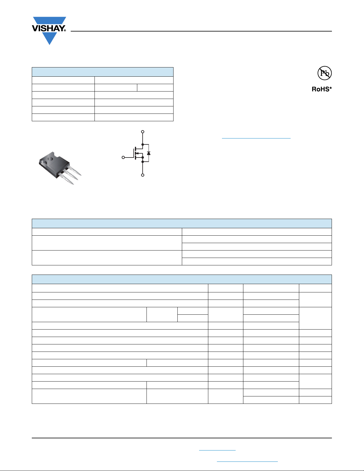
TO-247AC
G
D
S
IRFP26N60L, SiHFP26N60L
Vishay Siliconix
Power MOSFET
PRODUCT SUMMARY
VDS (V) 600
R
(Ω)V
DS(on)
Q
(Max.) (nC) 180
g
Q
(nC) 61
gs
Q
(nC) 85
gd
Configuration Single
= 10 V 0.21
GS
D
FEATURES
• Superfast body diode eliminates the need for
external diodes in ZVS applications
• Lower gate charge results in simpler drive
requirements
• Enhanced dV/dt capabilities offer improved ruggedness
• Higher gate voltage threshold offers improved noise
immunity
• Material categorization: for definitions of compliance
please see www.vishay.com/doc?99912
Note
*
Thi s datasheet pro vi des information about parts that are
G
RoHS-compliant and / or parts that are non-RoHS-compliant. For
example, parts with lead (Pb) terminations are not RoHS-compliant.
Please see the information / tables in this datasheet for details.
S
N-Channel MOSFET
APPLICATIONS
• Zero voltage switching (SMPS)
• Telecom and server power supplies
• Uninterruptible power supplies
• Motor control applications
ORDERING INFORMATION
Package TO-247AC
Lead (Pb)-free
SnPb
IRFP26N60LPbF
SiHFP26N60L-E3
IRFP26N60L
SiHFP26N60L
Available
Available
ABSOLUTE MAXIMUM RATINGS (TC = 25 °C, unless otherwise noted)
PARAMETER SYMBOL LIMIT UNIT
Drain-Source Voltage V
Gate-Source Voltage V
T
= 25 °C
Continuous Drain Current V
Pulsed Drain Current
a
at 10 V
GS
C
= 100 °C 17
C
DS
± 30
GS
I
D
IDM 100
Linear Derating Factor 3.8 W/°C
Single Pulse Avalanche Energy
Repetitive Avalanche Current
Repetitive Avalanche Energy
Maximum Power Dissipation T
Peak Diode Recovery dV/dt
Operating Junction and Storage Temperature Range T
Soldering Recommendations (Peak Temperature)
b
a
a
= 25 °C P
c
d
C
for 10 s 300
E
AS
I
AR
E
AR
D
dV/dt 21 V/ns
, T
J
stg
Mounting Torque 6-32 or M3 screw
Notes
a. Repetitive rating; pulse width limited by maximum junction temperature (see fig. 11).
b. Starting T
c. I
SD
d. 1.6 mm from case.
S15-0456-Rev. D, 16-Mar-15
= 25 °C, L = 1.7 mH, Rg = 25 Ω, IAS = 26 A, dV/dt = 21 V/ns (see fig. 12).
J
≤ 26 A, dI/dt ≤ 480 A/μs, VDD ≤ VDS, TJ ≤ 150 °C.
1
For technical questions, contact: hvm@vishay.com
THIS DOCUMENT IS SUBJECT TO CHANGE WITHOUT NOTICE. THE PRODUCTS DESCRIBED HEREIN AND THIS DOCUMENT
ARE SUBJECT TO SPECIFIC DISCLAIMERS, SET FORTH AT www.vishay.com/doc?91000
600
26
570 mJ
26 A
47 mJ
470 W
-55 to +150
10 lbf · in
1.1 N · m
Document Number: 91218
V
AT
°C
Page 2
IRFP26N60L, SiHFP26N60L
S
D
G
www.vishay.com
THERMAL RESISTANCE RATINGS
PARAMETER SYMBOL TYP. MAX. UNIT
Maximum Junction-to-Ambient R
Maximum Junction-to-Case (Drain) R
thJA
thCS
thJC
-40
0.24 -
-0.27
SPECIFICATIONS (TJ = 25 °C, unless otherwise noted)
PARAMETER SYMBOL TEST CONDITIONS MIN. TYP. MAX. UNIT
Static
Drain-Source Breakdown Voltage V
V
Temperature Coefficient ΔVDS/TJ Reference to 25 °C, ID = 1 mA - 0.33 - V/°C
DS
Gate-Source Threshold Voltage V
Gate-Source Leakage I
Zero Gate Voltage Drain Current I
Drain-Source On-State Resistance R
Forward Transconductance g
DS
GS(th)
V
GSS
DSS
VGS = 10 V ID = 10 A
DS(on)
fs
Dynamic
Input Capacitance C
Output Capacitance C
Reverse Transfer Capacitance C
Effective Output Capacitance C
Effective Output Capacitance
(Energy related)
Total Gate Charge Q
Gate-Drain Charge Q
Turn-On Delay Time t
Rise Time t
Turn-Off Delay Time t
Fall Time t
iss
- 450 -
oss
-34-
rss
eff.
oss
C
eff. (ER) - 170 -
oss
g
--61
gs
--85
gd
d(on)
r
-47-
d(off)
-42-
f
V
Drain-Source Body Diode Characteristics
Continuous Source-Drain Diode Current I
Pulsed Diode Forward Current
a
Body Diode Voltage V
Body Diode Reverse Recovery Time t
Body Diode Reverse Recovery Charge Q
Reverse Recovery Current I
Forward Turn-On Time t
S
I
SM
SD
rr
RRM
on
rr
MOSFET symbol
showing the
integral reverse
p - n junction diode
Notes
a. Repetitive rating; pulse width limited by maximum junction temperature (see fig. 11).
b. Pulse width ≤ 300 μs; duty cycle ≤ 2 %.
c. C
eff. is a fixed capacitance that gives the same charging time as C
oss
C
eff. (ER) is a fixed capacitance that stores the same energy as C
oss
VGS = 0 V, ID = 250 μA 600 - - V
VDS = VGS, ID = 250 μA 3.0 - 5.0 V
= ± 30 V - - ± 100 nA
GS
VDS = 600 V, VGS = 0 V - - 50 μA
V
= 480 V, VGS = 0 V, TJ = 125 °C - - 2.0 mA
DS
b
VDS = 50 V, ID = 16 A 13 - - S
VGS = 0 V,
V
= 25 V,
DS
f = 1.0 MHz, see fig. 5
= 0 V VDS = 0 V to 480 V
V
GS
= 26 A, VDS = 480 V,
I
= 10 V
GS
V
D
see fig. 7 and 15
= 300 V, ID = 26 A,
DD
R
= 4.3 Ω,VGS = 10 V
g
see fig. 11a and 11b
TJ = 25 °C, IS = 26 A, VGS = 0 V
c
b
b
b
TJ = 25 °C, IF = 26 A - 170 250
= 125 °C, dI/dt = 100 A/μs
T
J
TJ = 25 °C, IF = 26 A, VGS = 0 V
= 125 °C, dI/dt = 100 A/μs
T
J
b
b
b
TJ = 25 °C - 7.3 11 A
Intrinsic turn-on time is negligible (turn-on is dominated by LS and LD)
while VDS is rising from 0 % to 80 % VDS.
oss
while VDS is rising from 0 % to 80 % VDS.
oss
Vishay Siliconix
°C/WCase-to-Sink, Flat, Greased Surface R
-0.210.25Ω
- 5020 -
- 230 -
--180
-31-
- 110 -
--26
--100
--1.5V
- 210 320
- 670 1000
- 1050 1570
pF
nC Gate-Source Charge Q
ns
A
ns
nC
S15-0456-Rev. D, 16-Mar-15
THIS DOCUMENT IS SUBJECT TO CHANGE WITHOUT NOTICE. THE PRODUCTS DESCRIBED HEREIN AND THIS DOCUMENT
ARE SUBJECT TO SPECIFIC DISCLAIMERS, SET FORTH AT www.vishay.com/doc?91000
For technical questions, contact: hvm@vishay.com
2
Document Number: 91218
Page 3
www.vishay.com
I
D
, Drain-to-Source Current (A)
0.1
1
10
100
VDS, Drain-to-Source Voltage (V)
0.1
1
10
100
VGS
15 V
12 V
10 V
8.0 V
7.0 V
6.5 V
6.0 V
5.5 V
Bottom
Top
5.5 V
20 μs PULSE WIDTH
TJ = 150 °C
ID = 26 A
VGS = 10 V
TJ, Junction Temperature
R
DS(on)
, Drain-to-Source On Resistance (Normalized)
- 60 - 20- 40
0
20 40 60 80 100 120 140 160
0.5
1.0
1.5
2.0
2.5
3.0
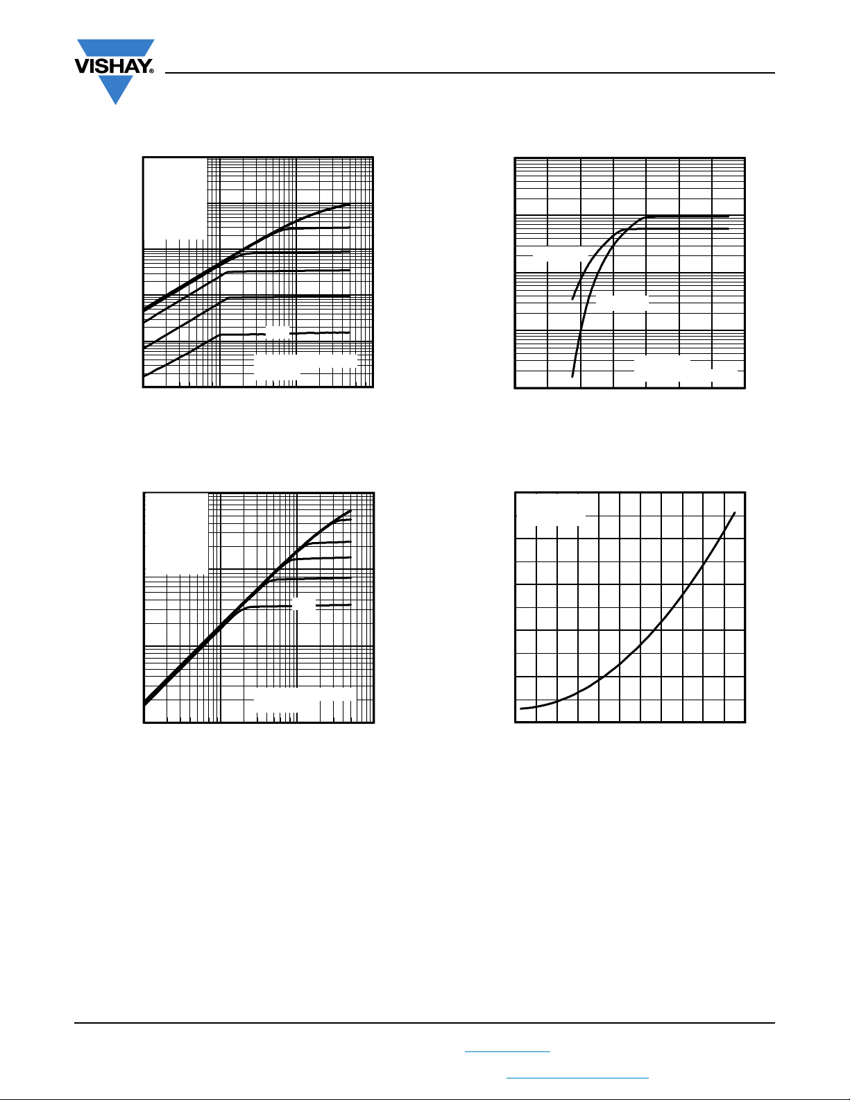
TYPICAL CHARACTERISTICS (25 °C, unless otherwise noted)
IRFP26N60L, SiHFP26N60L
Vishay Siliconix
1000
100
Top
Bottom
VGS
15 V
12 V
10 V
8.0 V
7.0 V
6.5 V
6.0 V
5.5 V
10
1
, Drain-to-Source Current (A)
D
I
0.1
0.01
0.1
VDS, Drain-to-Source Voltage (V)
Fig. 1 - Typical Output Characteristics
20 μs PULSE WIDTH
TJ = 25 °C
1
5.5 V
1000.00
100.00
TJ = 150 °C
10.00
TJ = 25 °C
, Drain-to-Source Current (A)
1.00
D
I
VDS = 50 V
0.10
2.0
4.0
10
100
6.0
20 μs PULSE WIDTH
10.0
8.0
12.0
14.0
16.0
VGS, Gate-to-Source Voltage (V)
Fig. 3 - Typical Transfer Characteristics
S15-0456-Rev. D, 16-Mar-15
THIS DOCUMENT IS SUBJECT TO CHANGE WITHOUT NOTICE. THE PRODUCTS DESCRIBED HEREIN AND THIS DOCUMENT
Fig. 2 - Typical Output Characteristics
ARE SUBJECT TO SPECIFIC DISCLAIMERS, SET FORTH AT www.vishay.com/doc?91000
Fig. 4 - Normalized On-Resistance vs. Temperature
3
For technical questions, contact: hvm@vishay.com
Document Number: 91218
Page 4

www.vishay.com
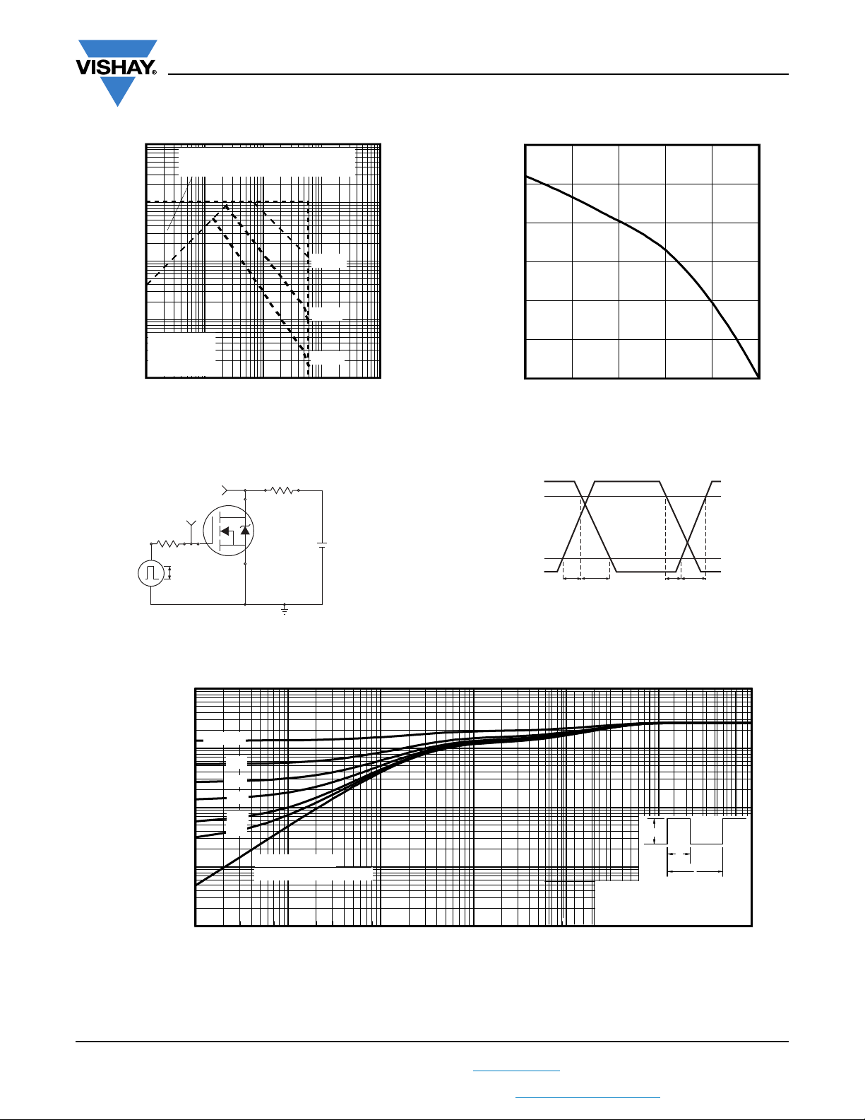
C
rss
C
oss
C
iss
VGS = 0 V, f = 1 MHz
C
iss
= Cgs + Cgd, Cds SHORTED
C
rss
= C
gd
C
oss
= Cds + C
gd
1
10
100
1000
10
100
1000
10000
1000000
C, Capacitance (pF)
VDS, Drain-to-Source Voltage (V)
VDS, Drain-to-Source Voltage (V)
Energy (µJ)
0
100
200
300
400
500
0
5
10
15
20
25
30
600
700
VSD, Source-to-Drain Voltage (V)
I
SD
, Reverse Drain Current (A)
1000.00
0.2
1.0
0.6
1.2
1.6
0.10
10.00
100.00
TJ = 150 °C
T
J
= 25 °C
1.00
0.4
0.8
1.4
V
GS
= 0 V
IRFP26N60L, SiHFP26N60L
Vishay Siliconix
12.0
10.0
8.0
6.0
4.0
, Gate-to-Source Voltage (V)
GS
V
2.0
ID = 26 A
VDS = 480 V
= 300 V
V
DS
= 120 V
V
DS
Fig. 5 - Typical Capacitance vs. Drain-to-Source Voltage
Fig. 6 - Typical Output Capacitance Stored Energy vs.V
DS
0.0
0
25
50
Qg, Total Gate Charge (nC)
100
125
75
150
Fig. 7 - Typical Gate Charge vs. Gate-to-Source Voltage
Fig. 8 - Typical Source-Drain Diode Forward Voltage
S15-0456-Rev. D, 16-Mar-15
THIS DOCUMENT IS SUBJECT TO CHANGE WITHOUT NOTICE. THE PRODUCTS DESCRIBED HEREIN AND THIS DOCUMENT
ARE SUBJECT TO SPECIFIC DISCLAIMERS, SET FORTH AT www.vishay.com/doc?91000
For technical questions, contact: hvm@vishay.com
4
Document Number: 91218
Page 5
www.vishay.com
Pulse width ≤ 1 µs
Duty factor ≤ 0.1 %
R
D
V
GS
R
G
D.U.T.
10 V
+
-
V
DS
V
DD
V
DS
90 %
10 %
V
GS
t
d(on)
t
r
t
d(off)
t
f
0.0001
0.001
0.1
1
1E-006
0.0001
0.001
0.1
t , Rectangular Pulse Duration (s)
Thermal Response (Z
thJC
)
0.01
0.02
0.05
0.20
D = 0.50
0.01
1E-005
1
0.10
SINGLE PULSE
(THERMAL RESPONSE)
t
1
t
2
Notes:
1. Duty factor D = t1/ t
2
2. Peak TJ = PDM x Z
thJC
+ T
C
P
DM
0.01
IRFP26N60L, SiHFP26N60L
Vishay Siliconix
1000
OPERATING IN THIS AREA LIMITED
BY R
DS(on)
100
10
, Drain Current (A)
D
I
1
= 25 °C
T
C
= 150 °C
T
J
Single Pulse
0.1
1
10
100
VDS, Drain-to-Source Voltage (V)
Fig. 9 - Maximum Safe Operating Area
100 µs
1 ms
10 ms
1000
10000
30
25
20
15
, Drain Current (A)
10
D
I
5
0
25
50
75
100
125
150
TC, Case Temperature (°C)
Fig. 10 - Maximum Drain Current vs. Case Temperature
S15-0456-Rev. D, 16-Mar-15
THIS DOCUMENT IS SUBJECT TO CHANGE WITHOUT NOTICE. THE PRODUCTS DESCRIBED HEREIN AND THIS DOCUMENT
Fig. 11a - Switching Time Test Circuit
Fig. 12 - Maximum Effective Transient Thermal Impedance, Junction-to-Case
For technical questions, contact: hvm@vishay.com
ARE SUBJECT TO SPECIFIC DISCLAIMERS, SET FORTH AT www.vishay.com/doc?91000
Fig. 11b - Switching Time Waveforms
5
Document Number: 91218
Page 6

www.vishay.com
TJ, Temperature (°C)
V
GS(th)
, Gate threshold Voltage (V)
-75
-50
-25 100
125
150
2.0
3.0
4.0
5.0
6.0
75
50
25
0
I
D = 250 μA
25
1050
900
750
600
450
0
150
125
100
75
50
I
D
TOP 12 A
16 A
BOTTOM 26 A
Starting TJ, Junction Temperature (°C)
E
AS
, Single Pulse Avalanche Energy (mJ)
300
150
Q
GS
Q
GD
Q
G
V
G
Charge
VGS V
IRFP26N60L, SiHFP26N60L
Vishay Siliconix
Fig. 13 - Threshold Voltage vs. Temperature
Fig. 14c - Maximum Avalanche Energy vs. Drain Current
15 V
L
D.U.T
I
AS
0.01
p
Ω
R
V
G
20 V
DS
t
Fig. 14a - Unclamped Inductive Test Circuit
Driver
+
V
A
DD
-
Fig. 15a - Basic Gate Charge Waveform
Current regulator
Same type as D.U.T.
V
I
AS
Fig. 14b - Unclamped Inductive Waveforms
S15-0456-Rev. D, 16-Mar-15
DS
t
p
12 V
V
GS
Fig. 15b - Gate Charge Test Circuit
6
50 kΩ
0.2 µF
0.3 µF
3 mA
I
G
Current sampling resistors
D.U.T.
I
D
Document Number: 91218
For technical questions, contact: hvm@vishay.com
THIS DOCUMENT IS SUBJECT TO CHANGE WITHOUT NOTICE. THE PRODUCTS DESCRIBED HEREIN AND THIS DOCUMENT
ARE SUBJECT TO SPECIFIC DISCLAIMERS, SET FORTH AT www.vishay.com/doc?91000
+
V
DS
-
Page 7

www.vishay.com
IRFP26N60L, SiHFP26N60L
Vishay Siliconix
Peak Diode Recovery dV/dt Test Circuit
D.U.T.
+
-
R
g
Driver gate drive
P.W.
+
-
Period
Circuit layout considerations
• Low stray inductance
• Ground plane
• Low leakage inductance
current transformer
• dV/dt controlled by R
• Driver same type as D.U.T.
I
controlled by duty factor “D”
•
SD
• D.U.T. - device under test
-
D =
g
P.W.
Period
+
+
V
DD
-
V
= 10 Va
GS
D.U.T. l
waveform
SD
Reverse
recovery
current
Re-applied
voltage
D.U.T. V
Inductor current
Note
a. V
waveform
DS
= 5 V for logic level devices
GS
Body diode forward
current
dI/dt
Diode recovery
dV/dt
Body diode forward drop
Ripple ≤ 5 %
V
DD
I
SD
Fig. 16 - For N-Channel
Vishay Siliconix maintains worldwide manufacturing capability. Products may be manufactured at one of several qualified locations. Reliability data for Silicon
Technology and Package Reliability represent a composite of all qualified locations. For related documents such as package/tape drawings, part marking, and
reliability data, see www.vishay.com/ppg?91218
S15-0456-Rev. D, 16-Mar-15
.
7
Document Number: 91218
For technical questions, contact: hvm@vishay.com
THIS DOCUMENT IS SUBJECT TO CHANGE WITHOUT NOTICE. THE PRODUCTS DESCRIBED HEREIN AND THIS DOCUMENT
ARE SUBJECT TO SPECIFIC DISCLAIMERS, SET FORTH AT www.vishay.com/doc?91000
Page 8
www.vishay.com
0.10 AC
M M
E
E/2
(2)
(4)
R/2
B
2 x R
S
D
See view B
2 x e
b4
3 x b
2 x b2
L
C
L1
1
2
3
Q
D
A
A2
A
A
A1
C
Ø k BD
M M
A
ØP
(Datum B)
ØP1
D1
4
E1
0.01 BD
M M
View A - A
Thermal pad
D2
DDE E
C
C
View B
(b1, b3, b5)
Base metal
c1
(b, b2, b4)
Section C - C, D - D, E - E
(c)
Planting
4
3
5
7
4
4
4
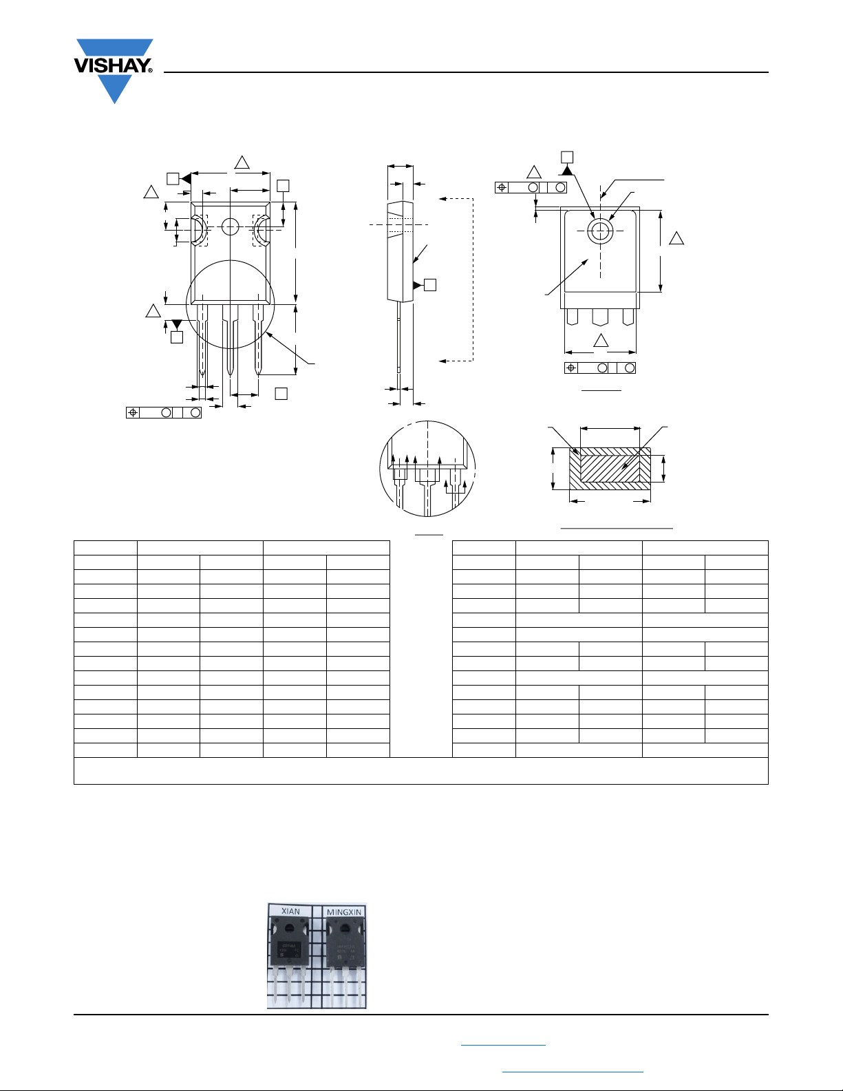
Lead Assignments
1. Gate
2. Drain
3. Source
4. Drain
Package Information
Vishay Siliconix
TO-247AC (High Voltage)
MILLIMETERS INCHES MILLIMETERS INCHES
DIM. MIN. MAX. MIN. MAX. DIM. MIN. MAX. MIN. MAX.
A 4.58 5.31 0.180 0.209 D2 0.51 1.30 0.020 0.051
A1 2.21 2.59 0.087 0.102 E 15.29 15.87 0.602 0.625
A2 1.17 2.49 0.046 0.098 E1 13.72 - 0.540 -
b 0.99 1.40 0.039 0.055 e 5.46 BSC 0.215 BSC
b1 0.99 1.35 0.039 0.053 Ø k 0.254 0.010
b2 1.53 2.39 0.060 0.094 L 14.20 16.25 0.559 0.640
b3 1.65 2.37 0.065 0.093 L1 3.71 4.29 0.146 0.169
b4 2.42 3.43 0.095 0.135 N 7.62 BSC 0.300 BSC
b5 2.59 3.38 0.102 0.133 Ø P 3.51 3.66 0.138 0.144
c 0.38 0.86 0.015 0.034 Ø P1 - 7.39 - 0.291
c1 0.38 0.76 0.015 0.030 Q 5.31 5.69 0.209 0.224
D 19.71 20.82 0.776 0.820 R 4.52 5.49 0.178 0.216
D1 13.08 - 0.515 - S 5.51 BSC 0.217 BSC
ECN: X13-0103-Rev. D, 01-Jul-13
DWG: 5971
Notes
1. Dimensioning and tolerancing per ASME Y14.5M-1994.
2. Contour of slot optional.
3. Dimension D and E do not include mold flash. Mold flash shall not exceed 0.127 mm (0.005") per side. These dimensions are measured at
the outermost extremes of the plastic body.
4. Thermal pad contour optional with dimensions D1 and E1.
5. Lead finish uncontrolled in L1.
6. Ø P to have a maximum draft angle of 1.5 to the top of the part with a maximum hole diameter of 3.91 mm (0.154").
7. Outline conforms to JEDEC outline TO-247 with exception of dimension c.
8. Xian and Mingxin actually photo.
Revision: 01-Jul-13
Document Number: 91360
1
For technical questions, contact: hvm@vishay.com
THIS DOCUMENT IS SUBJECT TO CHANGE WITHOUT NOTICE. THE PRODUCTS DESCRIBED HEREIN AND THIS DOCUMENT
ARE SUBJECT TO SPECIFIC DISCLAIMERS, SET FORTH AT www.vishay.com/doc?91000
Page 9

Legal Disclaimer Notice
www.vishay.com
Vishay
Disclaimer
ALL PRODUCT, PRODUCT SPECIFICATIONS AND DATA ARE SUBJECT TO CHANGE WITHOUT NOTICE TO IMPROVE
RELIABILITY, FUNCTION OR DESIGN OR OTHERWISE.
Vishay Intertechnology, Inc., its affiliates, agents, and employees, and all persons acting on its or their behalf (collectively,
“Vishay”), disclaim any and all liability for any errors, inaccuracies or incompleteness contained in any datasheet or in any other
disclosure relating to any product.
Vishay makes no warranty, representation or guarantee regarding the suitability of the products for any particular purpose or
the continuing production of any product. To the maximum extent permitted by applicable law, Vishay disclaims (i) any and all
liability arising out of the application or use of any product, (ii) any and all liability, including without limitation special,
consequential or incidental damages, and (iii) any and all implied warranties, including warranties of fitness for particular
purpose, non-infringement and merchantability.
Statements regarding the suitability of products for certain types of applications are based on Vishay’s knowledge of
typical requirements that are often placed on Vishay products in generic applications. Such statements are not binding
statements about the suitability of products for a particular application. It is the customer’s responsibility to validate that a
particular product with the properties described in the product specification is suitable for use in a particular application.
Parameters provided in datasheets and / or specifications may vary in different applications and performance may vary over
time. All operating parameters, including typical parameters, must be validated for each customer application by the customer’s
technical experts. Product specifications do not expand or otherwise modify Vishay’s terms and conditions of purchase,
including but not limited to the warranty expressed therein.
Except as expressly indicated in writing, Vishay products are not designed for use in medical, life-saving, or life-sustaining
applications or for any other application in which the failure of the Vishay product could result in personal injury or death.
Customers using or selling Vishay products not expressly indicated for use in such applications do so at their own risk.
Please contact authorized Vishay personnel to obtain written terms and conditions regarding products designed for
such applications.
No license, express or implied, by estoppel or otherwise, to any intellectual property rights is granted by this document
or by any conduct of Vishay. Product names and markings noted herein may be trademarks of their respective owners.
Revision: 13-Jun-16
1
Document Number: 91000
 Loading...